Modeling phase function of controlled diffraction elements on the basis of linear electro-optical effect

Author: Matyunin S.A., Paranin V.D., Levchenko V.I.
Journal: Сибирский аэрокосмический журнал @vestnik-sibsau
Section: Математика, механика, информатика
Article in issue: 5 (26), 2009.
Free access
A design of controlled diffractive optical elements based on electro-optic effect is suggested. The influence of the electro-optical crystal orientation, the direction of light wave propagation and the electric field distribution on the characteristics of controlled diffractive optical elements is considered. The efficiency indicators of controlled diffraction elements structure and material are proposed and their values for the basic elements are calculated.
Electrostatic field, electro-optical effect, controlled diffraction element
Short address: https://sciup.org/148176099
IDR: 148176099
Text of the scientific article Modeling phase function of controlled diffraction elements on the basis of linear electro-optical effect
Elements and devices based on the electro-optical effect are widely used to control parameters of optical illumination, e. g. intensity, phase, state of polarization, spectral composition [1]. Their advantages are high speed (GHz units), great nomenclature of functional materials with various physical properties. Volume and planar modulators, switchboards, deflectors of broadband and laser illumination, tunable spectral filters etc. are developed on the basis of the electro-optical effect at present.
Development of electro-optical controlled diffraction structures (CDS) with a tunable phase function [2–4] is one of the promising directions of creating devices of this kind. In general, the design of such elements includes electro-optical material, control electrodes with individual or group addressing ensuring the required distribution of the material as will as a complex of functional coatings possessing electro insulation, protective, spectroforming or polarization-selective functions (fig. 1).
Changing the kind of phase function with the help of single or multichannel voltage source results in forming a certain diagram of orientation of such a structure and changing its spectral composition.
The aim of this study is to model the phase function of controlled diffraction structures.
Since CDSs based on diffraction gratings form periodic structures a system of conventional symbols to designate the structures has been developed for the sake of convenience. The system of designations of controlled diffraction structures is based on constructional indicators of the basic element. By the basic element the elementary part of the structure is meant, which, repeated many times, forms CDS. The system takes into account the number and type of electrodes (continuous, discrete) on each surface of the element, the distraction of potentials over the electrodes, the presence of functional coatings. The following structural formula is proposed for the designation of basic optical elements:
N ( X 1 - Y 1 - Z 1 ): P 1
1 ( M 1 - R 1 - K 1 ): T 1
where N 1 is the number of times the basic structure is repeated; X 1, M 1 – the number of electrodes in the top (bottom) layer of the basic structure; Y 1 = { N D , R 1 = { N D is the type of electrodes in the top (bottom) layer (continuous N or D ); Z 1 indicates the potential distribution over the top (bottom) electrodes (0 for equal potentials of all electrodes, 1 for different potentials of electrodes); P 1 = {01, T 1= {01presence or absence of the functional top (bottom) layer of the basic structure.
Examples of the main types of basic elements with their designations and descriptions are given in table 1.
The analysis of the structure of electric fields in diffraction CDS shows that the field structure is quite complex, therefore the type of the electro-optical effect used essentially depends on the relationship between the CDS geometrical dimensions and properties of the electro-optical material. Because of this to assess the efficiency of the structure and of the type of electro-optical effect used local and integrated indicators of element efficiency have been stated: the indicator of the predominant type of electro-optical effect (1) and the indicator of CDS electro-optical efficiency (2). These indicators take into account both the structural design of the element and the properties of the electro-optical materials and control means chosen. They make it possible to optimize the parameters of the diffraction element controlled by a given indicator or a group of indicators:
g i j =
G = EE g- j = i =1 j =1 nm nm
EEI E tj n j |- EEI E X,' n jaX,j|
= =1 j =1 i =1 j =1 (2) nm nm
nm nm
EEIE,-EEIXl
i =1 j =1 i =1 j =1
nm nm
EEI Ej+EE ESI i=1 j=1 i=1 j=1
.
Variation of the values of local and integrated indicators gi,j and G ranges from minus one (–1) for the longitudinal (along the y coordinate axes) electro-optical effect to plus one (+1) for the transverse (along the x coordinate axis) electro-optical effect. Having set the threshold value of the indicator chosen (e. g. 0.1) we can obtain numerical assessment of the efficiency of the electro-optical diffraction element modeled.
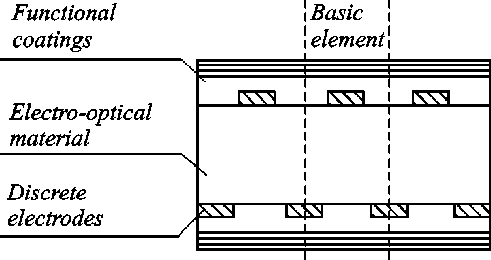
Optical wave direction
Fig. 1. General view of the controlled diffraction structure
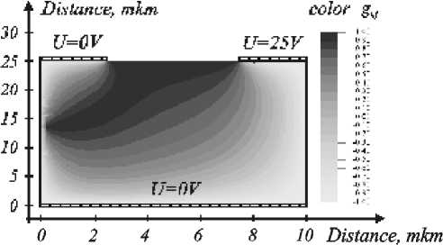
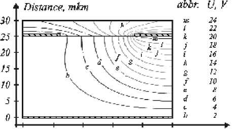
Figures 2 3 give examples of local efficiency indicator g ij distribution for basic elements of the type (2- D -1) and (2 , - B -1):1/(1- N - D ):
As can be seen from figure 2 the element (2- D -1):1 with the design and geometry parameters chosen provides
Examples of CDS basic element structures and their designations
Table 1
|
Symbol |
Designation short description |
Structure of the basic element |
|
1 - N - 0 1 - N - 0 |
Series structure with one top and one bottom continuous electrodes without functional layers |
|
|
2 - D - 1 1 - N - 0 |
Series structure with two discrete electrodes having different potentials in the top layer and one continuous electrode in the bottom layer without functional layers |
|
|
(2 - D - 1):1 1 - N - 0 |
Series structure with two discrete electrodes having different potentials in the top layer and one continuous electrode in the bottom layer with one top functional layer |
|
|
2 (2 - D - 1):1 1 - N - 0 |
Series-parallel structure consisting of two basic elements each of which comprises two discrete electrodes with different potentials in the top layer and one continuous electrode in the bottom layer as well as one top functional layer |
practically 100 percent transverse electro-optical effect in the central area and mixed effect in side areas. Therefore for the possibilities of the element in question to be used efficiently one should choose (by the value of the integrated indicator) the type and orientation of the electro-optical material which provide the transverse electro-optical effect.
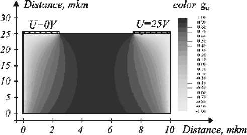
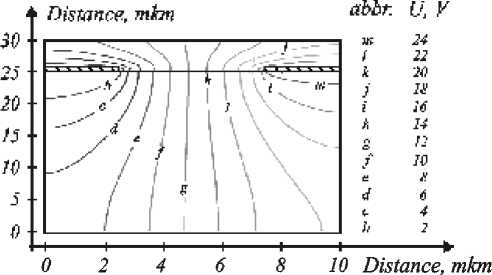
Fig. 2. Example of local efficiency indicator gi,j distribution in a basic element of the type (2- D -1):1
О 2 4 6 8 10 Distance, ткт
Fig. 3. Example of efficiency indicator gi,j distribution in a basic element of the type (2- B -1):1/(1- N - D )
The element of the type (2- B -1):1/(1- N - D ) from figure 3 provides mixed electro-optical effect in the interelectrode area, of predominantly by transverse nature in the upper part and of longitudinal nature in the lower part. Therefore, for the possibilities of the element in question to be used efficiently one should carry out additional investigation of electro-optical efficiency for various orientations of the crystal optical axis and the direction of optical radiation propagation in the crystal.
The element of this type is fundamentally different from the one discussed above in that it makes possible to obtain inclined linear or non-linear phase profiles since the areas of predominantly transverse and longitudinal effects have approximately triangular distribution.
For more precise mathematical modeling of processes in CDS the relationship is defined between the refractive index for a light wave with arbitrary direction and state of polarization on the one hand, and the type and orientation of the electro-optical crystal, the electric field intensity, on the other. As a result, a mathematical model has been developed that takes into account the change in the optical indicatrix of the electro-optical crystal when acted upon by the components of electric field in an arbitrary oriented crystal and the final formula is derived relating the value of refractive index n p2 to the initial data of the problem:
J ( k 2 z 2 b г - b 3 k 2 y 2 ) + ( b 3 k 2 x 2 - k 2 z 2 b i ) +( b i k 2 y 2 - k 2 x 2 b 2 )
P 2 ~ V B + C + D + E + F + H + J ’
B = b i b 3 k 2 x 2 k 2 y 2 d 3 - 2 b i b 3 k 2 x 2 k 2 z 2 c 2 + b k 2 x 2 c 2 ;
C = - b 2 b 3 k i2 d 3 + b 32 c i k 22 y 2 + b b 2 k 2 x 2 k 2 z 2 d i ;
D = - 2 b 2 b 3 k 2 y 2 k 2 z 2 c i + c i k 22 z 2 b 2 - b i b 3 d 2 k 2 y 2 ;
И 2 2 y 2 2 z 2 2 + i 2 y 2 c 3 2 x 2 2 y 2 3 i ;
F = — 2 k 2 x 2 k 2 y 2 b i b 2 c 3 + k 2 x 2 k 2 y 2 b 2 b 3 d 2 — k 2 x 2 k 2 z 2 b 22 d 2 ;
H = k Tx 2 b 2 c 3 - k 2 y 2 k 2 z 2 b i d 3 + k 2 y 2 k 2 z 2 b i b 3 d i ;
J = b i b 2 k 2 z 2 d i + k 2 x 2 k 2 z 2 b i b 2 d 3 + k 2,z 2 b i c 2
where k 2 x 2 , k 2 y 2 , k 2 z 2 are coordinates of the light wave vector in the coordinate system of the crystal and coefficients b 1, b 2, b 3, c 1, c 2, c 3, d 1, d 2, d 3 are:
_ f p 2 z 2 ( k 2 y 2 p 2 x 2 - k 2 x 2 p 2 y 2 )
bi = p 2 y 2 +—Г------------ ;
k 2 x 2p 2 z 2 k2 z 2p 2 x 2
P 2 x 2 ( k 2 y 2 p 2 x 2 - k 2 x 2 p 2 y 2 )
b2 =- p 2 x 2; b3 =--———;
k 2 x 2 P 2 z 2 k 2 z 2 P 2 x 2
c i =|^r + r ii Ex 2 + r i2 Ey 2 + r i3 E z 2 I ;
l Пх2
c 2 =
f
2 + r 2i E x 2 + r 22 E y 2 + r 23 Ez 2
l ny2
;
c 3 =1 2 + r 3i E x 2 + r 32 E y 2 + r 33 Ez 2 I ;
l nz2
d i = 2 ( r 6i Ex 2 + r 62 E y 2 + r 63 E z 2 ) ;
d 2 = 2 ( r 5i Ex 2 + r 52 Ey 2 + r 53 Ez 2 ) ;
d3 = 2 (rdEx2 + r42Ey2 + r43Ez2 ), where nx2, ny2, nz2 are refractive indices of the crystal in the absence of electric field; rlk are electro-optical coefficients, m/ V; Ex2, Ey2, Ez2 are field intensity projections along the crystal axis, V/m; p2x2, p2y2, p2z2 are polarization vector coordinates.
To calculate the electrostatic field in the anisotropic medium various methods of solution were analyzed: method of mirror images, method of conformal images as well as methods based on finite difference approximation. Eventually, preference was given to numerical methods as being the most universal ones. The Flex PDE 5.0 program using an adaptive triangular grid was used to calculate the electrostatic field in CDS. Software developed by the authors made it possible to define the phase function ф ( x ) at the output of CDS (taking into account the state of polarization p 2 x 2, p 2 y 2, p 2 z 2 and electro-optical coefficients rlk ):
2 n h
Аф(x) = ^JAn(Ea (x,y),Ec (x,y))dy (5) A0 0
where X 0 is the wavelength of radiation used, m; h is the thickness of the electro-optical material, m; A n is variation of refractive index under the influence of electrostatic field; Ea ( x , y ), Ec ( x , y ) are field intensity projections on a - and c - axes of crystal, respectively, V/m.
As a result of modeling it has been found that CDS of various types can be developed on the basis of structures like (2- B -1):1/(1- N - D ), for example, structures, dissipating illumination as well as controlled blazed diffraction structures if the electrostatic field intensity vector E x ( x , y ) between any two neighboring electrodes points in one direction.
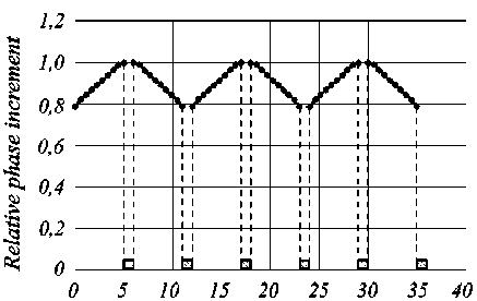
Figures 4, 5 show phase functions (5) for the basic element of the (2- B -1):1/(1- N - D ) type on the basis of a -cut of bariumstrontium niobate, SBN:75 grade, c -axis of which is perpendicular to the one-dimensional grid of control electrodes. The width of electrodes and the size of the diffraction slit was 5 mkm, electrode thickness was 0.5 mkm, the direction of light wave propagation was parallel to the x -axis of the crystal. The thickness of the protective coating (silicon dioxide) was 0.11 mkm.
From figures 4, 5 it follows that a change in the crystal thickness affects the electrostatic field distribution and the kind of phase function formed. As for changing the electrode potentials, it determines only the height of phase function profile, changes the diffraction efficiency of the element and restructures the CDS along the wavelength of illumination.
Figure 6 gives the phase function (5) of the element (2- D -1):1withthefollowingparameters: electro-opticalmaterial – barium-strontium niobate, SBN:75 grade, c -axis of which is perpendicular to the one-dimensional grid of control electrodes, the width of electrodes and the size of the diffraction slit is 5 mkm, electrode thickness is 0.5 mkm, the direction of light wave propagation is parallel to the a -axis of the crystal. The thickness of the protective coating (silicon dioxide) is 0.11 mkm.
Thus, it can be seen from figure 6 that:
-
– the kind of phase function formed is quasirectangular with the geometry defined by the width and period of arrangement of CDS electrodes;
-
– changing electrode potentials defines only the height of phase function profile.
Analysis of CDS with different crystal thickness has shown that for thickness of SBN:75 of the order of 2–3 CDS periods of electrode grid and more the kind of phase functions remains practically unchanged, i. e. approximately rectangular.
Thus model dependences obtained and calculations make it possible to announce the creation of a new class of tunable diffraction elements that realize phase functions of an arbitrary type, e. g. nearly rectangular, linear, square-law etc., which makes it possible to realize elements and devices performing the functions of switching modulation, deflection of optical radiation as well as changing (correction) of its directly diagram.
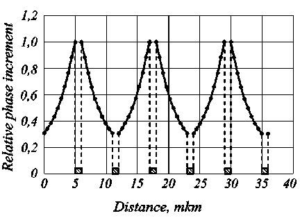
Fig. 4. Relative distribution of phase increment along the width of the diffraction slit of the element (2- B -1):1/(1- N - D ) with crystal thickness 11 mkm
Distance, mkm
Fig. 5. Relative distribution of phase increment along the width of the diffraction slit of the element (2- B -1):1/(1- N - D ) with crystal thickness 100 mkm
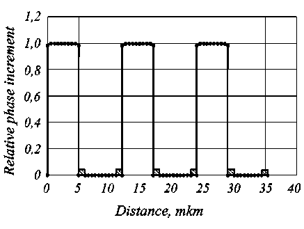
Fig. 6. Relative distribution of phase increment along the width of the diffraction slit of the element(2- D -1):1
with the crystal thickness 100 mkm
