Modular Design of 2n:1 Quantum Dot Cellular Automata Multiplexers and its Application, via Clock Zone based Crossover

Автор: Sonali Singh, Shraddha Pandey, Subodh Wairya
Журнал: International Journal of Modern Education and Computer Science (IJMECS) @ijmecs
Статья в выпуске: 7 vol.8, 2016 года.
Бесплатный доступ
Quantum-Dot Cellular Automata (QCA) is a radical technology, which works at Nanoscale. Due to its numerous advantages over the conventional CMOS-based digital circuits, researchers are now concentrating more on designing digital circuits using this technology. Researchers have reported various findings in this field till now. In this paper, a modular 2:1 Multiplexer has been designed followed by its application in the designing of 1-bit parallel memory. A 4:1 MUX is designed using cascading of two 2:1 multiplexers. This paper also incorporates a comparative analysis of the proposed circuits with some previous designs. This comparison indicates that the designed Multiplexer is showing a considerable reduction in cell count as well as in the area. Here the design and simulation of the circuits are done using QCA Designer Ver. 1.40. Power dissipation simulation analysis of the designed 4:1 multiplexer is also done using QCA Pro tool.
Quantum Dot Cellular Automata, Majority Gate, Multiplexer, Parallel Memory, Kink Energy
Короткий адрес: https://sciup.org/15014883
IDR: 15014883
Текст научной статьи Modular Design of 2n:1 Quantum Dot Cellular Automata Multiplexers and its Application, via Clock Zone based Crossover
For the reduction of area and cost of digital circuits, VLSI industry is now considering the scaling of circuits to Nano scale levels. CMOS-based digital circuits can be scaled up to a specific limit; beyond that limit further scaling of CMOS is not possible because below that limit CMOS devices show unusual characteristics. Due to this reason, researchers are now concentrating on finding new techniques which can be used at Nanoscale to design digital circuits and QCA is one such technology. At present QCA can be considered as the most outstanding substitute for CMOS technology. There are several advantages of this technology like [1] -1.The speed of operation is very high, 2.Power consumption is low, 3. Device density is high.
The multiplexer is a combinational circuit which permits picking one output amid numerous inputs. It transfers one of the inputs to the output at a time, so it is also known as Data selector. This type of operation facilitates to share one costly device for more than one application in a system.
Due to its abundant use, it has become necessary to implement a multiplexer circuit which is area efficient which results in the reduction of the cost of designing. Till now various QCA based Multiplexers have been designed [2] to [6]. QCA structures are mostly designed using coplanar wire crossing. However, this type of wire crossing is enormously prone to external effects as well as crosstalk [7].In [8] a successful attempt is reported to design a multiplexer circuit without using coplanar wire crossing. In [9], three clock zones based approach is used to design a modular multiplexer. In this paper also, a modular 2:1 MUX and using that 2:1 MUX a 4:1 MUX is also designed. By cascading of this 2:1 MUX, any higher order MUX can be designed.
The remaining part of this paper is as follows. In II section, background material of QCA technology is discussed. In III section, the work related to the multiplexer circuit is reported. In IV section design of 1 Bit Parallel memory using proposed 2:1 multiplexers is discussed. In V section, an application of 2:1 MUX is demonstrated. In section VI, power dissipation analysis of proposed 4:1 MUX is done.Simulation results are discussed in Section VII. In the end, VIII section concludes the paper.
-
II. Background Material
The principle of Quantum Dot Cellular was first proposed by Lent et al. in the year 1993 [10].QCA is a
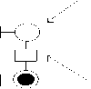
novel emerging technology in which logic states are not stored as voltage levels, but rather the position of the individual electron [1]. In QCA, binary information is represented by bi-stable charge configuration. The fundamental unit of Quantum Dot Cellular Automata is QCA Cell. A QCA cell is shown in Fig 1. Each QCA cell contains four quantum dots at the corner of the cell and electrons reside in two of the Quantum Dots. Electrons reside at diagonally opposite quantum dots, because at that position, Coulomb repulsion force is least. Polarization P measures the extent to which the charge distribution is aligned along one of the diagonal axes. If the charge density on a dot i is pi then the polarization is defined in (1) [11] [12]:
( pl+p3 )( p2+p4 ) pl+p2+p3+p4
B
A
O
C
Fig.3. QCA Majority Gate
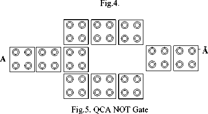
Functioning of AND Gate and OR Gate can be obtained from this Majority gate by setting one of the input to logic 0 and logic 1 as shown in Fig 4 (a) and (b) respectively. In addition to this, Not Gate functioning is obtained by using QCA inverter circuit as shown in Fig 5. All digital circuit can be designed using these two logic primitives.
-
A. Logic Sates
In QCA, logic states are represented by two possible charge configurations. A basic QCA Cell is shown in Fig. 1. QCA cells representing Logic 0 and Logic 1 are shown in Fig. 2(a) and 2(b) respectively. Cell representing logic 0 has polarization P = -1 and cell representing logic 1 has polarization P = +1.
-
B. QCA Devices
The Coulomb interaction force between the cells associates the state of one cell to the state of neighbor cells. Due to this interaction, neighboring cells coordinate their polarization. The primeval logic gate in QCA is Majority Logic Gate. It consists of 5 QCA cells, arranged in a plus sign manner as shown in Fig. 3. It has three inputs, one output, and a driver cell. The logic function of Majority gate is shown in (2).
A

B
-1. 00

O
O
+1.00
B


Maj(A, B. C) = AB + BC +AC (2)
a). QCA AND Gate
b). QCA OR Gate
Electron charge
Quantum Dot
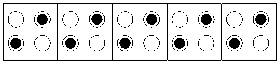
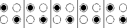
In QCA, information transmits from one place to another in QCA binary wires. QCA binary wires are constructed from an array of cells having the same polarization as shown in Fig 6.

Capacitor
Logic1
Logic1

Tunnel juncion
Logic0
Logic0
Fig.6. QCA Binary Wire


Fig.1. A QCA Cell

b).Logic 1
a).Logic 0
Fig.2.
-
C. QCA Clock
Clocking of QCA is suggested in [13]. In QCA, clocking is a crucial parameter; it is used for providing power to the circuit and also for controlling the flow of information. The clock signal is generated by the application of an electric field to the cell, which raises or lowers the tunneling barrier between the quantum dots in
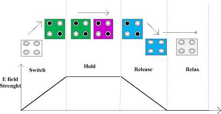
the cell which enables the transfer of electrons between the cells. Clocking (by application of an appropriate voltage to a cell) leads to adjustment of tunneling barriers between quantum dots for transfer of electrons between the dots [14]. In QCA, clocking is accomplished by two techniques: zone clocking and continuous clocking. In Zone Clocking [15], each clock has four clock phases are used: switch, hold, release and relax as shown in Fig. 7. Color coding for different cells is shown in Fig. 8.
Switch phase -In the beginning, cells remain in the unpolarized state and have low potential barriers, then barriers are raised.
Hold phase - In this phase, potential barriers are kept high.
Release phase -In this phase, potential barriers are brought down.
Relax phase -In this phase potential barrier of the cells kept at low state and cells remain in the unpolarized state.
In Continuous clocking, potential field is generated by the system of submerged electrodes.
Time
Fig.7. Clock Phases in Zone Clocking.
® I ® ® I
@1® I # I ® ®
Clock 2 Clock 3 Output
Input Clock 0 Clock 1
Fig.8. Color coding of clocks in Zone Clocking
-
III. Related Work
In [2] Kyosun Kim et al. have analyzed the causes of the failure of QCA circuits and have proposed an adder circuit which utilizes a multiplexer. Proper clocking scheme is exploited in this design. They have told that the state of a multiple input QCA design depends on all the inputs which result in a variety of sneak noise paths in QCA. So they systematically analyzed the sneak noise paths in QCA- based design by using the concept of kink energy. And this analysis is significant due to its influence as the design size grows. They have also analyzed the failure of majority gates, and then they used the coplanar clocking technique in the design of full adder to overcome the errors. The multiplexer which has been used by them uses clock gating which is faster and smaller.
In [3] Mardirisi and Karafyllidis have proposed modular 2 to 1 multiplexer which is formulated to increase the circuit stability. They have used the concept of crossover design for signal propagation and have shown each logic gate with a block. Each block consists of two pairs of cells serially connected which produces signal delay equal to the number of included cell pairs. Their proposed design of 2:1 MUX consists of 56 cells and area is about 0.07μm2. They have also shown a 4:1 MUX which consists of 215 cells covering an area of inputs is 6 clock phases i.e. 1.5 clock cycles.
In [4] Hashemi et al. have proposed multiplexer in three layers in which the first layer is the backbone of the circuit. This new design is denser with four clocks latency and faster. Also a 4:1MUX has shown 33% improvement in reducing complexity and 28% improvement in the area. The proposed structure is reliable at high frequency when the number of inputs becomes larger.
In [5] Roohi et al. have designed 2:1 multiplexer using three clock zones due to this delay have been increased.
In [6] Sen et al. have proposed a modular design of 2:1 MUX that in turn used to synthesize 4:1 and 8:1 MUX. The design of 2:1 MUX is efficient as having less delay and involving only two clock zones. The improvement in 4:1 MUX and 8:1 MUX is about 27.9% and 27% respectively. They have done the power dissipation analysis of 8:1 MUX and shown that the circuit is energy efficient. They have also discussed fault tolerant behavior of the multiplexer circuits. For this purpose, they have used the HDLQ Verilog library to convert the QCA equivalent in hardware description language. Their proposed design produces an average of 77.62% correct outputs even when the design is faulty.
Although many researchers have done remarkable work in the field of design of multiplexers but still the circuit is not competent with the current trend of area constraint. And this force to think and develop an efficient design of 2:1 MUX, which can be further used to design any complex logic. And thus in this paper the proposed design of 2:1 MUX is proved to be efficient regarding the number of cells consumed, and the area required. Also the power dissipation analysis of the 4:1 MUX is done to check the power consumption of the design.
-
IV. Proposed Multiplexer Design
The multiplexer is an essential digital circuit. It has many applications like it is used in the design of memory and FPGA circuits and it can also be used to implement many Boolean functions. It has 2 inputs, one output and n select lines, which transfers one of input to the output based on the value of the select lines. Many eminent researchers have shown the structure of multiplexer and gave valid statements regarding its benefits. The proposed design of multiplexer in [6] uses only two zones of clocking scheme i.e. clock 0 and clock 1. Based on similar approach, here two different designs of 2:1 MUX have been proposed. Moreover the proposed structure is competent as well as powerful in terms of number of cells used to design the circuit. Additional efforts are done here in order to make promising structure of the multiplexer in terms of number of cells used and area occupied by the design.
-
A. 2:1 MUX
The conventional circuit of 2:1 MUX has two Data inputs I0 and I1, one select line S and one output Out. The truth table is given in Table 1, and the block diagram is shown in Fig. 9. The Logic function of Output O is given in (3).
O = I0S̅ + I1S (3)
Table 1. Truth table of 2:1MUX
|
S |
O |
|
0 |
I0 |
|
1 |
I1 |
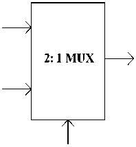
S0
Fig.9. Graphical symbol of 2:1 MUX
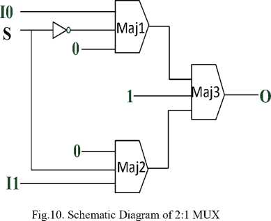
The output equation reveals that the MUX can be implemented using two AND gates, one NOT Gate and one OR Gate. One inverter and three Majority Gates are required to design this MUX. The QCA equivalent block diagram is shown in Fig.10. The majority based output expression of this circuit is given in (4).
^^^^^^^
O = Maj( Maj(I0, S̅, 0), Maj(I1, S, 0), 1 ) (4)
1st proposed structure-
The first method to design 2:1 MUX is shown in Fig. 11 which enables us to get the output by using only two zones of one clock cycle. The proposed circuit is efficient in terms number of cells used. Therefore, the area occupied by the design is also less.
2nd proposed structure
In this approach, the number of cells used is only one less than the first one, but the schematic is quite different regarding the arrangement of cells. Its QCA layout is shown in Fig. 12. Here total 18 QCA cells are used to design the circuit.
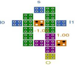
Fig.11. QCA Layout of 2:1 MUX (1st Proposed Structure)
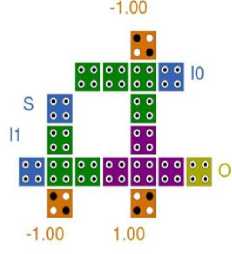
Fig.12. QCA Layout of 2:1 MUX (2nd Proposed Structure)
The functioning of all the logic gates using the proposed 2:1 MUX can be seen from below lemmas.
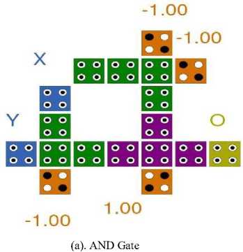
Lemma 1 - A 2:1 MUX can be used to implement a two-input AND Gate.
Proof : Put select line S =X, inputs I0=0 and I1=Y. Then 2:1 mux implements AND operation of inputs X and Y i.e. Out=X.Y.
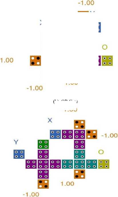
Lemma 2- A 2:1 MUX can be used to implement a two-input OR Gate.
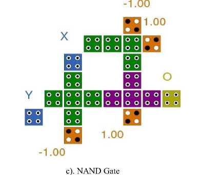
Lemma 3- A 2:1 MUX can be used to implement 1 two input NAND gate.
Proof: Put select line S=X and Inputs I0= 1 and
I1=Y̅.Then 2:1 mu x implements NAND operation of X and Y i.e. Out=X. Y.
Lemma 4: A 2:1 MUX can be used to implement a two-input NOR gate.
Proof: Put select line S=X and inputs I0=Y̅ and I1=0. Then 2:1 m ux implements NOR operation of X and Y i.e. Out=X + Y.
Lemma 5: A 2:1 MUX can be used to implement a two-input EXOR gate.
Proof: Put select line S=X and inputs I0= Y and I1=Y̅ Then 2:1 MUX implements XOR operation of X and Y i.e. Out= X ⊕ Y
Lemma 6: A 2:1 MUX can be used to implement a two-input XNOR gate.
Proof: Put select line S=X and inputs I0=Y̅, Then 2:1 mux imple ments XNOR operation of X and Y i.e.
Out=X ⊕ Y
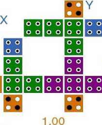
The QCA layout of the all the logic gates are shown in Fig. 13 from (a) to (f).
-1.00
d). NOR Gate
-1.00
(b). OR Gate
-1.00
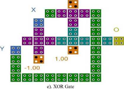
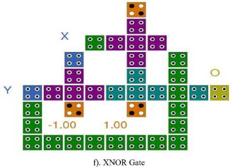
Fig.13. (a to f): QCA Layout of all the Logic Gates
-
B. 4:1 MUX
4:1 MUX has four data inputs I0, I1, I2 and I3, two select lines S0 and S1 and one output O. Output of this MUX is given in (5).
" ---------- -------------
Out = I0̅S̅1̅̅S̅0̅̅ + I1̅S̅1̅ S0 + I2S1̅S̅0̅̅ + I3S1S0 (5)
Table 2. Truth Table of 4:1 MUX
|
S1 |
S0 |
OUT |
|
0 |
0 |
I0 |
|
0 |
1 |
I1 |
|
1 |
0 |
I2 |
|
1 |
1 |
I3 |
Fig.15. Schematic of proposed 4:1 MUX
If 4:1MUX is designed directly using (4), then it will require 15 majority gates. However, if some modification is done in the above equation, the same functionality can be obtained using only nine majority gates as shown in (6).
Out = I0̅S̅1̅̅S̅0̅̅ + I1̅S̅1̅ S0 + I2S1̅S̅0̅̅ + I3S1S0
-
= ̅S̅1̅(I0̅S̅0̅ + I1S0) + S1(I2̅S̅0̅ + I3S0 (6)
Above output expression using majority logic is shown in (7).
Out = M(M(̅S̅1̅, (M(I0, ̅S̅0̅, 0), M(I1, S0,0), 1)), 0), (M(̅S̅1̅, (M(I0, ̅S̅0̅, 0), M(I1, S0,0), 1)), 0), 1) (7)
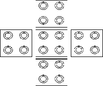
The proposed 4:1 Mux has been designed by cascading three 2:1 Mux as shown in Fig 15.Its schematic and QCA layout is shown in Fig. 14 and Fig. 16 respectively. In this design clock zone based crossover [16] is used. This recently discovered clock zone based crossover is very robust and fast in operation and has very low cost as described in [17] and [18]. In this approach, the phase difference between two clock zones of the two crossed wires is 180 degrees.
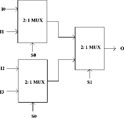
Fig.14. 4:1 MUX using 2:1 MUX
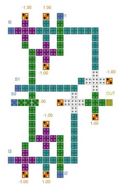
Fig.16. QCA Layout of proposed 4:1 MUX
-
V. Design Of 1 Bit Parallel Memory Using Proposed 2:1 Mux
The parallel memory cell is a fundamental and commonly used module in several digital circuits. Parallel memory enables us to access all the bits of the data word concurrently with low latency because it consists of several 1-bit memory loops. The drawback of the parallel memory is that for higher order memory, a lot of circuitry is repeated, so complexity and area of the circuits are increased considerably. Due to this, parallel memories are not chosen where the compact circuit is required. So any optimization in its complexity and area is appreciated. In paper[19] memory is designed using four dot 1 QCA, but simulation result is not reported in that paper, similarly, a parallel memory circuit presented in paper [20], designed using two dot 1 electron. Here the same approach is used to design 1-bit parallel memory which comprises of two AND Gates and one 2:1 MUX and to meet the area challenge; the parallel memory is designed by using the 2nd proposed 2:1 MUX and its block diagram are represented in Fig. 17.
Table 4. Truth Table of Parallel Memory
|
Chip Sel |
Rd’/Wt |
Input |
Output |
|
0 |
0 |
0 |
0 |
|
0 |
0 |
1 |
0 |
|
0 |
1 |
0 |
0 |
|
0 |
1 |
1 |
0 |
|
1 |
0 |
0 |
previous output(0) |
|
1 |
0 |
1 |
previous output(0) |
|
1 |
1 |
0 |
Input(0) |
|
1 |
1 |
1 |
Input(1) |
Rd’/Wt
Chip Sel
Fig.17. 1 Bit Parallel Memory [20]
From the block diagram, it can be seen that two input signals control the operation of this memory chip. One input signal (Chip Sel) is used for chip selection, it activates or deactivates the memory chip and the other input (Rd’/Wt) are used for selecting memory read, or memory write operation. The two inputs of 2:1 MUX act as data to be read or write in the memory. Whenever Chip Sel=0 memory is in reset mode, i.e., output=0. To perform a memory read or memory write operation, first of all, set Chip Sel=1. Now, for memory read operation set Rd’/Wt=0 then input I0 is selected. As it is connected to the output of MUX which is the previously stored value of the memory, so, in this case, the data to be read is available at the output. And for memory write operation set Rd’/Wt=1, so select line of the MUX will be 1 and input I1 will be selected. The data to be written is applied at the input I1, and therefore, the write operation is done in this case. The operation of the memory can be easily understood by its Functional table and truth table are shown in Table 3 and Table 4 respectively-
Table 3. Functional Table of Parallel Memory
|
Chip Sel |
Rd’/Wt |
Memory operation |
|
0 |
X |
Reset |
|
1 |
0 |
Memory read |
|
1 |
1 |
Memory write |
The majority based block diagram of the parallel memory using proposed 2:1 MUX is shown in Fig. 18. The QCA layout requires five majority gates and one inverter as shown in Fig. 19. By using our proposed 2:1 multiplexer, the number of cells as well as the area occupied by the design is reduced, which shows its dominance over other designs.
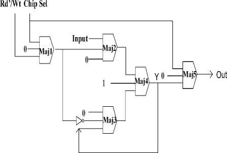
Fig.18. Schematic of proposed 1 Bit Parallel Memory
Majority based equation of this memory is shown in (8).
Out = M5(M4(M2(Input, M1(Rd/Wt, ChipSel,0)
,0),M3(M1,Y,0),1),1),ChipSel,0)
Rd'/Wt chip se!
^В
В 1 °0
В ВВ
BQ EQ ^Q^QQQEQEQ - ■ - • EQFQ
в в100 в щ щ out
■MB ЯМЙ input ^ЙЯЕВ®......... •
№ О О
-1 00 1.00
Fig.19. QCA Layout of Proposed Parallel Memory
-
VI. Computation Of Power Dissipation In Proposed 4:1 Multiplexer
Kink energy plays a vital role in calculating the power dissipation of QCA structures. Kink energy Eк , is the energy required by the circuit to excite the system from the ground state to first excited state [1]. Kink energy is directly related with power dissipation and on the other hand, it is inversely related to the steady state polarization error. So to make a tradeoff between power dissipation and polarization error, we need to set an optimum kink energy value to get acceptable values for both power dissipation as well as for polarization error.
For computing power dissipation of QCA structures, the probabilistic modeling tool- QCA Pro is used. It provides a GUI (Graphical User Interface) based on Bayesian Network [21, 22]. This tool generates an equivalent thermal model for each QCA cell. There will be some hot spots in the thermal model; the color represents the amount of power dissipated i.e. the one which will be black in color dissipates maximum power and goes on decreasing the dissipated power as the color lightens up. Switching power loss in QCA circuits is calculated using the Upper Bound Model [23].Thermal equivalent model of proposed 4:1 multiplexer is shown in Fig. 20. Its shows this MUX is dissipating very less power because it contains only two hot spots. Power dissipation at the time of switching is analyzed for three values of kink energy as shown in Table 5. Average energy dissipation in the circuit increases with the increase of kink energy which can be seen from the graph in Fig. 21.
Table 5. Analyzed Parameters Value in Power Dissipation Analysis
|
Parameter |
Kink Energy (m eV) |
||
|
.5 |
1 |
1.5 |
|
|
Max Kink Energy |
0.00218 Ek |
0.00218 Ek |
0.00218 Ek |
|
Max Energy dissipation of circuit |
0.44898 |
0.45678 |
0.53314 |
|
Max Energy dissipation vector |
1 2 |
1 2 |
2 1 |
|
Avg Energy dissipation of circuit |
0.26002 |
0.31218 |
0.40734 |
|
Max Energy dissipation among all cells |
0.01155 |
0.01081 |
0.01066 |
|
Max Energy dissipation vector |
1 0 |
3 1 |
0 1 |
|
Min Energy dissipation of circuit |
0.05065 |
0.15080 |
0.26856 |
|
Min Energy dissipation vector |
0 0 |
3 3 |
3 3 |
|
Avg Leakage Energy dissipation |
0.05168 |
0.15372 |
0.27264 |
|
Avg Switching Energy Dissipation |
0.20834 |
0.15847 |
0.13469 |

Fig.20. Thermal Equivalent Model of 4:1 MUX
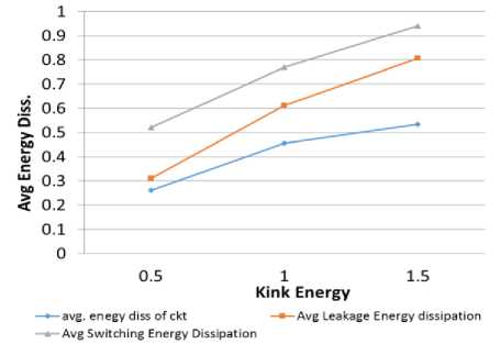
Fig.21. Avg. Energy Dissipation vs. Kink energy
-
VII. Simulation Results And Discussion
For designing and simulation of the circuits, QCA Designer Ver. 2.0.3 is used using Bistable Approximation Engine with default parameters.
-
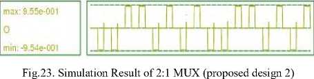
A. Simulation result of 2:1 MUX
Simulation results of proposed 2:1 multiplexer design1 and design2 are shown in Fig. 22 and 23 respectively. Here input S is given bit stream 00001111; input I1 is given bit stream 00110011 and input I0 is given bit stream 01010101 hence at the output O bit stream 01010011 is obtained. From the output, it can be observed that for the first four clock cycles select line S is
zero the output O is following the input I0 for these four cycles, and when select line S is becoming 1 for next four clock cycles, the output O is following input I1. So the simulation result reveals the fact that the proposed circuits are showing the behavior of 2:1 Multiplexer. A comparative analysis of proposed 2:1 MUX is given in Table 6. This analysis indicates that the proposed structure is better than all other previous design in terms of cell count and area consumed. So It can be said that the designed MUX is efficient than all other previous designs.
Table 6. Comparison of 2:1 Multiplexers-
min: -9.54e-001 U U Ц U U U U L
Fig.22. Simulation Result of 2:1 MUX (proposed design 1)
max: 1.OOe+OOO
S---- min: -1 .OOe+OOO ____________________________________________________ max: 1 .OOe+OOO
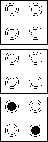
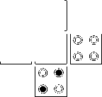
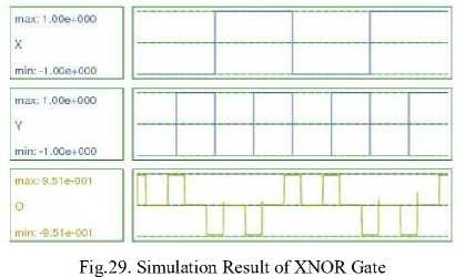
Y. Input X is given bit stream 00110011, and input Y is given bit stream 01010101.So at the AND Gate output O, bit stream 00010001 is obtained as shown in Fig. 24. At the OR Gate output O, bit stream 01110111 is obtained as shown in Fig.25. Similarly, at NAND gate output, bit stream 11101110 and at NOR gate output bit stream 10001000 are obtained as shown in Fig. 26 and 27 respectively. At XOR Gate output, bit stream 01100110 and at XNOR Gate output, bit stream 10011001 are obtained as shown in Fig. 28 and 29. For AND, OR and NAND Gates 2 clock zones are used, so for these gates, output has been obtained without any latency. On the hand, for NOR, XOR and XNOR gates three clock zones are used, and latency of 0.5 clock cycle is seen at the output, as the effect of inputs is reaching the output after 0.5 clock cycle.
max: 1 .OOe+OOO
И --------------- min: -1 .OOe+OOO ___L_J___L_ J L_J___L_ J_________________
B. Simulation Results of all the Logic Gates using 2:1 MUX
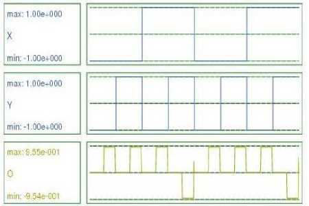
Fig.26. Simulation Result of NAND Gate
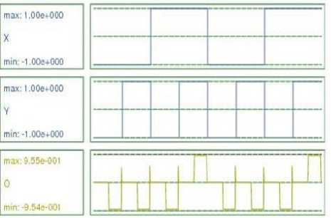
Fig.24. Simulation Result of AND Gate
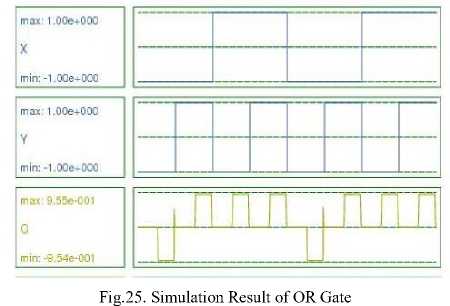
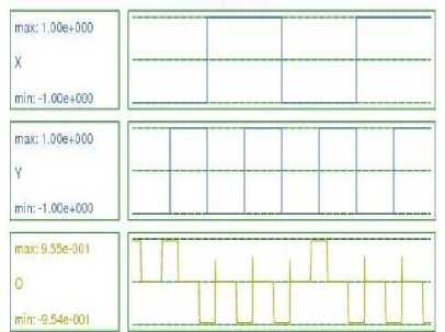
Fig.27. Simulation Result of NOR Gate
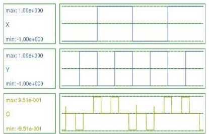
Fig.28. Simulation Result of XOR Gate
-
C. Simulation result of 4:1 MUX
Simulation result of proposed 4:1 MUX is shown in Fig. 30. Here select line inputs S1 and S0 are given bit streams 001100110011 and 010101010101 respectively. Data inputs are given following bit streams, I0 is given
000010001000, I1 is given 010001000100, I2is given 001000100000 and I3 is given 010010001010. At the output O, bit stream X01101110110 is obtained. From the simulation result, it can say that the output is following input I0 when S1=0 and S0=0, it is following input I1 when S1=0 and S0=1, it is following input I2 when S1=1 and S1=0 and it is following input I3 when S1=1 and S0=1. Hence, this circuit is showing the logic behavior of 4:1 MUX. There is a latency of 1 clock cycle at the output as the input is reaching to the output after the delay of one clock period. Comparison of proposed 4:1 MUX with some previously designed MUX is done. This comparison is presented in Table 7.This analysis is verifying the fact that the proposed structure is efficient than all other designs.
Table 7. Comparison of 4:1 Multiplexers-
|
Design |
Cell Count |
Area (μ m ) |
Clock Zones |
|
In [8] |
271 |
0.37 |
19 |
|
In [3] |
215 |
0.25 |
6 |
|
In [6] |
155 |
0.24 |
5 |
|
Proposed |
114 |
0.17 |
5 |
-
D. Simulation Result of 1 Bit Parallel Memory
Simulation result of 1-bit parallel memory is shown in Fig. 31. Chip Sel. is given bit stream 0000111100001111.Rd’/Wt is given bit stream 0011001100110011 and input are given bit stream 0101010101010101.At MUX output bit stream X000000011111110 is obtained and at the memory output bit stream X000000010000110 is obtained. The memory output is 0 when Chip Sel. =0 i.e. memory is in a reset mode in this case. When Chip Sel. =1 and Rd’/Wt =0 memory is following the output of the multiplexer, which is the previously stored value of the memory i.e. memory read operation is accomplished in this case. When Chip Sel=1, Rd’/Wt=1 and Input= Data to be written in the memory, the output of the memory is following the input i.e. memory write operation is accomplished in this case. In this way, the circuit is showing the behavior of 1 Bit parallel memory. Here also latency of one clock cycle is seen in the output.
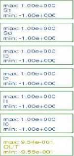
Fig.30. Simulation Result of 4:1 MUX
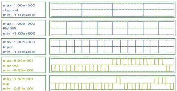
Fig.31. Simulation Result of 1 Bit Parallel Memory
-
VIII. Conclusion
This paper proposes novel design approach of 2:1 MUX circuit using 4 Dot 2 Electron QCA. This approach has the capability to implement any higher order multiplexer and therefore using proposed 2:1 MUX, an efficient 4:1MUX is designed. Power dissipation analysis of the designed 4:1 MUX is done which is proclaiming the fact that the designed MUX is power efficient i.e. dissipating very less power, In order to demonstrate the utility of the proposed 2:1 MUX a 1- Bit Parallel Memory has been implemented. The proposed designs have shown significant improvements in comparison to the previously designed multiplexers in terms of area and complexity. Also, the circuit is having less delay than the other previous designs. Here robust coplanar clock zone based crossover is used to construct the QCA circuits that result in a reduction of QCA cell count and area consumption without any latency overhead.
Список литературы Modular Design of 2n:1 Quantum Dot Cellular Automata Multiplexers and its Application, via Clock Zone based Crossover
- J Haung, and F Lombardi,"Design and test of digital circuits by quantum-dot cellular," Boston, MA (2008).
- Kim K, Wu K, and Karri R,"The robust QCA adder designs using composable QCA building blocks," IEEE Trans Comput-Aid Design Integrated Circuit System, Vol. 26, pp.176–83, 2007.
- VA Mardiris and IG Karafyllidis,"Design and simulation of modular 2n QCA multiplexer," International Journal of Circuit Theory and Applications, Vol. 38, Issue 8, pp. 771-785, September 2010.
- S. Hashemi, M. R. Azghadi and A Zakerolhosseini, "A Novel QCA multiplexer design". Telecommunications, 2008. IST 2008. International Symposium on," pp. 692–695,2008. http://dx.doi.org/10.1109/ISTEL.2008.4651389.
- A Roohi, H Khademolhosseini,S Sayedsalehi, and K Navi, "A novel architecture for quantum-dot cellular automata multiplexer," International Journal of Computer Science Vol. 8, Issue 6, 2011.
- Bibhash Sen, Mrinal Goswami, Subhra Mazumdar, and Biplab K Sikdar, "Towards the modular design of reliable quantum- dot cellular automata logic circuit multiplexers." Microelectronics Journal of Computers & Electrical Engineering, Vol. 45, pp. 42–54, 2015.
- A. Chaudhary et al. "Fabricatable interconnect and molecular QCA circuits," IEEE Transactions on Computer-Aided Design of Integrated Circuits and Systems, Vol.26, Issue 11, pp. 1978 – 1991, Nov. 2007.
- R. Sabbaghi, Nadooshan and, M. Kianpour. "A novel QCA implementation of MUX-based universal shift registers," Journal of Computational Electronics, Vol. 13, Issue 1, pp. 198-210, March 2014.
- B. Sen, M.Dutta, D.Sara,B Sikdar,"An efficient multiplexer in quantum-dot cellular automata", Progress in VLSI Design and Test. Lecture Notes in Computer Science, Berlin Heidelberg: Springer, vol. 7373,pp.350–351,2012.doi.org/10.1007/978-3-642-31494-0_40.
- C.S. Lent, P.D. Tougaw, and W. Porod, "Bistable saturation in coupled quantum dots for quantum cellular automata", Applied Physics Letter, Vol.62, pp.714-716, 1993.
- C. S Lent et al., "Quantum cellular automata," Nanotechnology, Vol. 4, No. 1, pp. 49-57,1993.
- P. D Tougaw. and C. S. Lent, "Logical devices Implemented using Quantum Cellular Automata," Journal of Applied Physics, Vol. 75, No. 3, Feb 1994.
- K. Walus and G.A. Jullien, "Design tools for an emerging SoC technology: quantum-dot cellular automata". Proceedings of the IEEE, Vol. 94, Issue 6 pp.1225–1244, June2006.
- K Sridharan and Vikram Pudi." Design of Arithmetic Circuits in Quantum Dot Cellular Automata Nanotechnology," Publisher : Springer International, Year:2015
- C.S. Lent, P.D. Tougaw, "A device architecture for computing with quantum dots". Proceedings IEEE, Vol. 85, Issue 4, pp.541–557,1997.
- D. Abedi, G. Jaberipur, and M. Sangsefidi, "Coplanar Full Adder in Quantum-Dot Cellular Automata via Clock-Zone Based Crossover,"IEEE Transactions on Nanotechnology, Vol. 14, Issue 3, pp. 497 - 504 doi:10.1109/TANO.2015.2409117
- M. SangSefidi, D. Abedi, and M. Moradian. "Design a Collector with More Reliability against Defects during Manufacturing in Nanometer Technology, QCA." Journal of Software Engineering and Applications, Vol. 6, Issue 6, pp. 304-312, 2013.
- S.-H. Shin, J.-C. Jeon, and K.-Y. Yoo, "Wire-crossing technique on quantum-dot cellular automata," In NGCIT2013, the 2nd International Conference on Next Generation Computer and Information Technology, Vol. 27, pp. 52–57,2013.
- D. Agrawal and B. Ghosh, "Quantum Dot Cellular Automata Memories", International Journal of Computer Applications, Vol. 46, Issue. 5, 2012.
- Mili Ghosh, Debarka Mukhopadhyay, and Paramartha Dutta. "A Novel Parallel Memory Design using 2 Dot 1Electron QCA," 2015 IEEE 2nd International Conference on Recent Trends in Information Systems (ReTIS), Kolkata, India.
- Sanjukta Bhanja, and Sudeep Sarkar. "Probabilistic Modeling of QCA Circuits Using Bayesian Networks," IEEE Transactions on Nanotechnology, Vol. 5, Issue 6, pp. 657 - 670, DOI: 10.1109/TNANO.2006.883474
- Saket Srivastava, and Sanjukta Bhanja. "Hierarchical Probabilistic Macromodeling for QCA Circuits," IEEE Transactions on Computers, Vol.56, pp. 174-190,2007.
- Saket Srivastava, Sudeep Sarkar, and Sanjukta Bhana, "Estimation of Upper Bound of Power Dissipation in QCA Circuits," IEEE Transactions on Nanotechnology, 2008, Vol. 8, Issue: 1 pp. 116 – 127, DOI: 10.1109/TNANO.2008.2005408.
