Nanophotonic structure formation by dry e-beam etching of the resist: resolution limitation origins
Автор: Rogozhin Alexander Evgenyevich, Bruk Mark Avramovich, Zhikharev Evgeny Nikolaevich, Sidorov Fedor Alekseevich
Журнал: Компьютерная оптика @computer-optics
Рубрика: Opto-it
Статья в выпуске: 4 т.41, 2017 года.
Бесплатный доступ
A wide range of structures for nanophotonics and optoelectronics can be formed by dry e-beam etching of the resist (DEBER). High resist sensitivity due to chain depolymerization reaction provides efficient etching with high throughput of the method. The structures obtained by the DEBER in this research are well-rounded diffraction gratings, binary gratings and staircase profiles. The major disadvantage of DEBER is poor lateral resolution, which may be caused by different physical mechanisms. Four groups of possible mechanisms leading to the resolution limitation are determined and the influence of some mechanisms is estimated.
Deber, e-beam etching, nanophotonics, diffractive optical elements, diffractive optics, three-dimensional lithography, three-dimensional fabrication, microlithography, optical design and fabrication
Короткий адрес: https://sciup.org/140228634
IDR: 140228634 | DOI: 10.18287/2412-6179-2017-41-4-499-503
Текст научной статьи Nanophotonic structure formation by dry e-beam etching of the resist: resolution limitation origins
Dry electron beam etching of resist (DEBER) proposed by Bruk et. al. [1, 2] could be used for formation of wide range of optoelectronic and photonic structures. The method is based on the chain depolymerization reaction, which takes place in the polymer resists during e-beam exposure at the glass-transition or higher temperatures. The volatile reaction products (monomers) are pumped out during exposure. The method provides quite simple way for formation of well-rounded or 3D structures. In some cases, it could be much more flexible than usual methods, in others it could be more productive or convenient. Similar phenomena were observed in PMMA during ion beam irradiation [3] and UV radiation [4].
PMMA sensitivity to e-beam in the DEBER method is about 100 times higher than that in the standard “wet” e-beam lithography process. Because of high vertical resolution (about 1 nm) the method could be used for high-precision 3D structuring. On the other hand, DEBER lateral resolution (about 200 nm) and contrast (0.7 – 1.5) are rather low. It is difficult to use DEBER method for nanophotonic structure fabrication due to low lateral resolution. For nanophotonic applications the lateral resolution of the formation method should be lower than 100 nm [5, 6].
It is not clear which physical mechanism leads to the lateral resolution limitation. It seems that most of the possible mechanisms are the same for DEBER and ordinary e-beam lithography [7, 8, 9] but their contribution to the lateral resolution lowering should be reconsidered.
In this paper structures of diffraction or binary gratings, some diffractive optical elements (DOE), 3D structures or planar photonic crystals obtained by DEBER method are presented. Also in the paper, different mechanisms that could lead to the broadening of the trenches are analyzed. The influence of several mechanisms on DEBER lateral resolution is estimated.
1. Dry e-beam etching of resist
The DEBER method is based on the chain depolymerization reaction which takes place in the polymer resists during e-beam exposure at the glass-transition or higher temperatures. Volatile reaction products (monomers) are pumped out during exposure (Fig. 1). Various resists that could be effectively decomposed to monomer under these conditions can be used in the method (poly(methyl methacrylate), poly-α-methylstyrene, polymethyl isopropenyl ketone etc.).
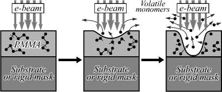
Fig. 1. Dry e-beam etching of resist process scheme
In the DEBER method at a temperature higher than glass-transition temperatures e-beam stimulated chain depolymerization reaction takes place. In this process polymer bonds are broken during e-beam exposure. As a result, molecules of terminal macroradicals are formed. These macroradicals at increased temperatures split off monomer molecules one by one with “zipper” mechanism [2, 10]. Lots of monomer molecules are evacuated during exposure. The process is faster at higher temperatures. The relief (trenches or holes) formation is defined by appearance in the exposed region free space due to evacuation of volatile monomers and polymer relaxation as affected by surface tension. Well-rounded shape of the structures is determined by a specific form of the etching kinetic curves (Fig. 2) of DEBER method [11].
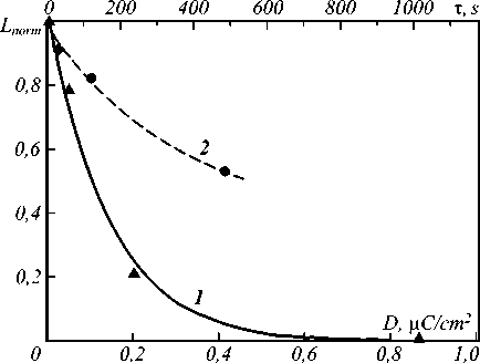
Fig. 2. DEBER kinetic curves for PMMA: normalized “etching depth vs. exposure dose” dependence; initial PMMA thickness are 900 nm (curve 1) and 340 nm (curve 2); exposure in Camscan S4 system at 160°C
DEBER process could be implemented in some scanning electron microscopes (SEM), e-beam lithography or focused e-beam induced process (FEBIP) systems. Most of the systems require minor modifications for it. It is possible to transfer relief after DEBER process from the resist to the silicon or fused silica substrate or to the metal mask [11].
2. Optoelectronic and photonic structures obtained by DEBER method
DEBER method could be effective for the formation of diffraction or binary gratings, some diffractive optical elements (DOE), 3D structures or planar photonic crystals [13].
It is difficult to use DEBER method for nanostructure fabrication due to low lateral resolution. It is not clear which physical mechanism leads to the lateral resolution limitation. We used two scanning electron microscopes in our study: Camscan S4 with 200 nm ebeam diameter and Zeiss Ultra-55 with 10 nm e-beam diameter. PMMA 950K (Allresist AR-P 672.05) have been used as a resist. Dry e-beam etching of resist in the first system provided 2000 nm wide trenches. In the second system 200 nm wide trenches were obtained at the same process parameters.
Simple gratings obtained by DEBER method are quite similar to holographic gratings (Fig. 3 a ). They also have sinusoidal shape and limited efficiency. Throughput for DEBER method is lower than ruling or holographic method but it is high enough for small gratings production. DEBER exposure time of 3×3.9 mm2 is about 10100 s (exposure dose 0.1-1 μC/cm2). DEBER method is extremely accurate due to e-beam system exploitation. Moreover, the shape of the grating produced by DEBER method could be modified. The shape of the grooves could be skewed, for example. Also, complex grating like binary gratings could be produced by DEBER method if e-beam lithography or FEBIP system is used. Large set of positive resists could be used with DEBER method.
Diffractive optical elements (DOE) contain staircase structures. Formation of staircase structures by DEBER
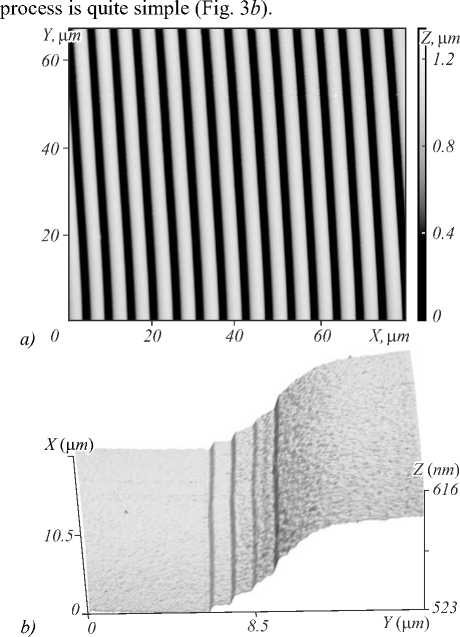
Fig. 3. AFM images of the (a) diffraction grating and (b) staircase structure obtained by DEBER method
The technique is similar to grayscale e-beam lithography. But due to specific etching mechanism vertical resolution of the DEBER method is 1-2 nm. DEBER is a one-step process and misalignment also does not take place for the method. The method also is comparatively high-productive.
Drawbacks of DEBER method here are edge rounding and low lateral resolution. Edge rounding leads to insignificant efficiency decrease [14]. It appears that if the DEBER method is implemented in the modern e-beam lithography or FEBIP system lateral resolution will be enough for DOE fabrication.
DEBER method could be used not just for simple diffraction grating formation but also for formation of complex binary gratings or planar photonic crystals (Fig. 4). In this case DEBER works like standard e-beam lithography with limited lateral resolution. On the other hand, it seems that edge rounding could somewhat decrease efficiency of these structures.
3. Origins of the DEBER resolution limit
There are several possible mechanisms of the line broadening. We split them into four groups: products of the e-beam interaction events; chemical mechanisms; mechanical processes and thermal mechanisms.
-
3.1. Products of the e-beam interaction events
In this group, we placed e-beam scattering and particle generation due to scattering events. In the DEBER process the sensitivity of the resist at low doses is extremely high. As a result, tails of the electron distributions could play essential role into the broadening of the line.
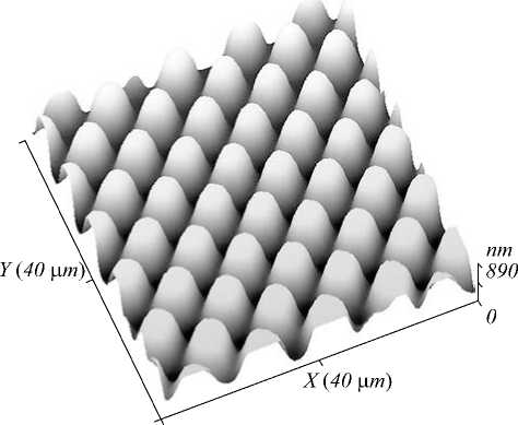
Fig. 4. 3D AFM image of structure obtained by DEBER method during exposure of two sets of lines
Four different types of events of the interaction between primary electrons and the matter can be separated [15]. They are elastic scattering and three types of inelastic scattering-generation of secondary electrons, plasmons or excitation (which lead to generation of high energy photons or Auger electrons). These events determine the ways of energy transfer from fast electrons to the photoresist. It should be mentioned that the contribution of plasmon generation mechanism to the electron energy loss is very high but plasmon appearance results only in the heat generation but not any molecular transitions.
Because of elastic scattering of the primary electrons fast electrons can find way to the distant regions of the resist layer. We calculated primary electron trajectories using CASINO program [16] in the PMMA/Si structures (Fig. 5) and found that primary electrons can be easily found in 6 μm wide region around the position of e-beam.
In the DEBER process resist is extremely sensitive to low doses (it can be seen from the Fig. 2) and energy of electrons can be as low as 10 eV. Potentially elastic scattering could lead to the lines broadening. But elastic scattering cannot be the reason of the trench width difference for 15 nm and 200 nm wide e-beams.
The secondary electrons have the largest contribution to the distribution of electron energy deposition in the photoresist [15 n]. To carefully analyze the contribution of the secondary electrons in the line broadening their distributions should be calculated. It is not a simple task and it requires lots of time. In this work, we only estimated it using data from the literature. Energy distribution of secondary electrons is somehow described in [17, 18]. The mean energy of “fast” secondary electrons (energy higher than 100 eV) is about 400 eV for primary electron energy of 20 keV [19]. It seems that the number of secondary electrons with energy higher than 1 keV is negligible. So, in the worst case the generation of secondary electrons can results in 30-40 nm broadening of trench.
a)
b)
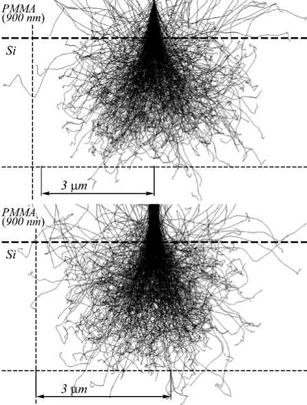
Fig. 5. Trajectories of 500 electrons during e-beam irradiation of the PMMA (900 nm)/Si structure calculated in the CASINO program. E-beam diameters are 15 nm (a) and 200 nm (b).
Electron energy is 20 keV
Estimation of the contribution of high energy photons into trench broadening is a large task. The lowest possible wavelength of characteristic radiation for 20 keV e-beam is about 0.06 nm. The peak of intensity is somewhere between 0.09 and 0.12 nm. PMMA absorption of this radiation is very low (Fig. 6). On the other hand, characteristic radiation with wavelength of 2-8 nm (corresponds to energy of secondary electrons) could provide trench broadening observed in the experiments. In any case influence of the characteristic radiation should be accurately calculated. Doping of the PMMA could soften the characteristic radiation influence.
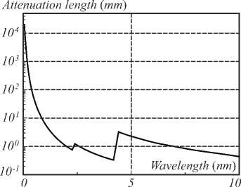
Fig. 6. Attenuation length of X-ray in PMMA vs. wavelength (data from [13])
-
3.2. Chemical mechanisms
-
3.3. Mechanical processes
-
3.4. Thermal mechanisms
The second group of processes contains different chemical mechanisms. Two most probable are chain transfer and diffusion of the reaction products along the resist layer.
Chain transfer is the chemical reaction leading to transfer of the depolymerization process from one PMMA chain to another. Usually the process takes place by hydrogen abstraction [13]. In this case interacting chains should not be far from each other. It appears that the distance between them should be less than 1-5 nm. If the size of PMMA chain is about 15-20 nm (for 950K PMMA), 40-50 chain transfer processes are required for 1 μm trench broadening. It appears that the probability of this event is not high enough.
The diffusion of the reaction products can also spread depolymerization process in the distant regions of PMMA. Some products are too heavy for the diffusion (for example, long chain parts and large radicals) but monomer molecules and short chain fragments could be mobile enough. In concert with chain transfer diffusion could provide substantial trench broadening. These mechanisms require detailed analysis and calculations.
Polymer chemistry is rather complex and embarrassed. It is possible that there are some other chemical mechanisms of depolymerization spreading. Additional experiments and chemical analysis are necessary for understanding of these mechanisms.
Chemical mechanisms could be partially blocked by use of PMMA with lower molecular weight. Also, the process parameters like temperature play significant role in chemical mechanisms.
In this group, there is a phenomenon connected with low viscosity of PMMA at the process temperatures. At the temperature, higher than glass transition one the viscosity of the polymer drops dramatically. This process makes outdiffusion of monomer possible. So, it is important for the DEBER process. On the other hand, at these temperatures liquidity can lead to redistribution of the PMMA and as a result trench broadening. Some additional experiments are required to analyze this phenomenon. Lowering of temperature could soften the influence of the resist liquidity. It seems that the process of the resist redistribution is quite slow. Therefore, it is not very important for short processes.
Thermal mechanism relates to possible lack of temperature uniformity in PMMA and warming up of the sample during exposure. It is not clear if this mechanism is important. Additional research is required.
Conclusion
DEBER method could be used for formation of wide range of optoelectronic and photonic structures. In this paper structures of diffraction or binary gratings, some diffractive optical elements (DOE), 3D structures or planar photonic crystals obtained by DEBER method are presented.
It is difficult to use DEBER method for nanophotonic structure fabrication due to low lateral resolution. It is not clear which physical mechanism leads to the lateral resolution limitation. In the paper, different mechanisms that could lead to the broadening of the trenches are analyzed. Possible influence of e-beam scattering, generation of secondary electrons and high energy phonons, chemical mechanisms and fluidity of PMMA is estimated.
Primary electron tracks in PMMA/Si structure were simulated in CASINO program, which allowed us to suppose that primary electron scattering can’t be the reason for the trench broadening observed. Besides, the contribution to the DEBER resolution limitation caused by plasmon generation seems to be negligible. The trench broadening due to secondary electrons is estimated as 3040 nm. The characteristic radiation could be the reason for the resolution limitation observed and its contribution need to be accurately calculated. Chemical mechanisms (chain transfer and diffusion processes) also may lead to trench broadening, which require additional analysis. The other possible mechanisms which may contribute to the resolution limitation are based on low viscosity of PMMA at the process temperature and possible lack of temperature uniformity in PMMA during the experiment.
Список литературы Nanophotonic structure formation by dry e-beam etching of the resist: resolution limitation origins
- R.F. Patent of Invent RU 2478226 C1 G 03 F 7/00, C 08 F 8/50. Method of forming masking image in positive electron resists /M.A. Bruk, E.N. Zhikharev, V.A. Kal'nov, A.V. Spirin, D.R. Strel'tsov, filed September 06, 2011, published of March 27, 2013, Russian Bull. of Inventions N9, 2013.
- Bruk, M.A. The new dry method of mask (relief) formation by direct electron-beam etching of resist/M.A. Bruk, E.N. Zhikharev, D.R. Streltsov, V.A. Kalnov, A.V. Spirin//Microelectronic Engineering. -2013. -Vol. 112(C). -P. 1-4. - DOI: 10.1016/j.mee.2013.06.003
- Fragalà, M.E. Ion beam assisted unzipping of PMMA/M.E. Fragalà, G. Compagnini, L. Torrisi, O. Puglisi//Nuclear Instruments and Methods in Physics Research Section B: Beam Interactions with Materials and Atoms. -1998. -Vol. 141, Issue 1-4. -P. 169-173. - DOI: 10.1016/S0168-583X(98)00087-1
- Mita, I. Photoinitiated thermal degradation of polymers II. Poly(methyl methacrylate)/I. Mita, K. Obata, K. Horie//Polymer Journal. -1990. -Vol. 22. -P. 397-410. - DOI: 10.1295/polymj.22.397
- Kemme, S. Microoptics and nanooptics fabrication/S. Kemme. -Boca Raton, FL: Taylor & Francis Group, 2010. -232 p. -ISBN: 978-0-8493-3676-8.
- Photonics, Volume 2: Nanophotonic structures and materials/Ed. by D.L. Andrews. -Hoboken, New Jersey: John Wiley & Sons, 2015. -424 p. -ISBN: 978-1-118-22551-6.
- Broers, A.N. Electron beam lithography -Resolution limits/A.N. Broers, A.C.F. Hoole, J.M. Ryan. -Microelectronic Engineering. -1996. -Vol. 32, Issue 1-4. -P. 131-142. - DOI: 10.1016/0167-9317(95)00368-1
- Vieu, C. Electron beam lithography: Resolution limits and applications/C. Vieu, G. Carcenac, A. Pepin, Y. Chen, M. Mejias, A. Lebib, L. Manin-Ferlazzo, L. Couraud, H. Launois//Applied Surface Science. -2000. -Vol. 164, Issue 1. -P. 111-117. - DOI: 10.1016/S0169-4332(00)00352-4
- Manfrinato, V.R. Determining the resolution limits of electron-beam lithography: Direct measurement of the point-spread function/V.R. Manfrinato, J. Wen, L. Zhang//Nano Letters. -2014. -Vol. 14, Issue 8. -P. 4406-4412. - DOI: 10.1021/nl5013773
- Bruk, M.A. Radiation-induced depolymerization of PMMA adsorbed on silochrome/M.A. Bruk, M.V. Kondrat'eva, A.A. Baranov, K.V. Pebalk, A.M. Sergeev, N.V. Kozlova//Polymer Science Series A. -1999. -Vol. 41, Issue 2. -P. 159-164.
- Bruk, M.A. Formation of micro-and nanostructures with well-rounded profile by new e-beam lithography principle/M.A. Bruk, E.N. Zhikharev, A.E. Rogozhin, D.R. Streltsov, V.A. Kalnov, S.N. Averkin, A.V. Spirin//Microelectronic Engineering. -2016. -Vol. 155. -P. 92-96. - DOI: 10.1016/j.mee.2016.03.017
- Rogozhin, A.E. Dry e-beam etching of resist for optics/A.E. Rogozhin, M.A. Bruk, E.N. Zhikharev, D.R. Streltsov, A.V. Spirin, J. Hramchihina//Journal of Physics: Conference Series. -2016. -Vol. 741, Issue 1. -012115. - DOI: 10.1088/1742-6596/741/1/012115
- Han, G. Comprehensive model of electron energy deposition/G. Han, M. Khan, Y. Fang, F. Cerrina//Journal of Vacuum Science & Technology B. -2002. -Vol. 20, Issue 6. -2666. - DOI: 10.1116/1.1526633
- Hovington, P. CASINO: A new monte carlo code in C language for electron beam interaction -part I: Description of the program/P. Hovington, D. Drouin, R. Gauvin//The Journal of Scanning Microscopies: Scanning. -1997. -Vol. 19, Issue 1. -P. 1-14. - DOI: 10.1002/sca.4950190101
- Dapor, M. Comparison between Energy Straggling Strategy and continuous slowing down approximation in Monte Carlo simulation of secondary electron emission of insulating materials/M. Dapor//Progress in Nuclear Science and Technology. -2011. -Vol. 2. -P. 762-768. - DOI: 10.15669/pnst.2.762
- Lee, K.W. Secondary electron generation in electron-beam-irradiated solids: Resolution limits to nanolithography/K.W. Lee, S.M. Yoon, S.C. Lee, W. Lee, I.-M. Kim, C.E. Lee, D.H. Kim//Journal of the Korean Physical Society. -2009. -Vol. 55, Issue 4. -P. 1720-1723. - DOI: 10.3938/jkps.55.1720
- Henke, B.L. X-ray interactions: photoabsorption, scattering, transmission, and reflection at E=50-30000 eV, Z=1-92/B.L. Henke, E.M. Gullikson, J.C. Davis//Atomic Data and Nuclear Data Tables. -1993. -Vol. 54, Issue 2. -P. 181-342. - DOI: 10.1006/adnd.1993.1013

