Novel Current-Mode All-Pass Filter with Minimum Component Count

Author: Jitendra Mohan, Bhartendu Chaturvedi, Sudhanshu Maheshwari
Journal: International Journal of Image, Graphics and Signal Processing(IJIGSP) @ijigsp
Article in issue: 12 vol.5, 2013.
Free access
In this paper, two novel first order current-mode all-pass filters are proposed using a resistor and a grounded capacitor along with a multi-output dual-X second-generation current conveyor (MO-DXCCII). There is no element matching restriction. Both the circuits exhibit low input and high output impedance, which is a desirable feature for current-mode circuits. The proposed circuits are simulated using SPICE simulation program to confirm the theory.
Analog signal processing, DXCCII, current-mode, all-pass filter
Short address: https://sciup.org/15013149
IDR: 15013149
Text of the scientific article Novel Current-Mode All-Pass Filter with Minimum Component Count
Published Online October 2013 in MECS (http://www.
Current-mode (CM) circuits have become popular due to their advantages such as wider dynamic range, inherent wider bandwidth, simple circuitry and low power consumption over the voltage-mode counterparts [1]. On the other hand, a CM circuit with features of low input and high output impedance is of special interest as there is no need for additional circuitry or active element for cascading or interfacing within a system and it also decreases the number of active elements in the system. First order all-pass filters (APF) are very useful building block for many analog signal processing applications such as for the realization of multiphase oscillators, high Q band pass filters, phase equalizers and also for introducing frequency dependent delay while keeping the amplitude of the input signal constant over a frequency range of interest. Recently, the design of first-order current-mode all-pass filter (CMAPF) has received attention for the use of minimal number of active and passive components (i.e. one active element and two passive components).
Numerous first-order CMAPF circuits were proposed using different types of current-mode active building blocks in the literature [2-15]. Some of these circuits are based on single active element [3-5, 7-10, 12, 14]. The reported single active element based circuits as described in [3-5, 7, 10, 12] employ more than two passive components, but show the feature of high output impedance suited for CM cascading. Moreover the circuits described in [6, 11, 13-14] fall in category of tunable, resistorless realizations. The most recent of these described in [14] shows low input and high output impedance feature with single active element and one capacitor. The circuit described in [8] employs one current differencing buffered amplifier (CDBA), one capacitor and one resistor. However, its input impedance is not low and the capacitor used is not grounded. The circuit given in [2] employs two active elements. The circuits presented in [5, 9] are based on minimal component count, but require additional current conveyor to sense the output current. The recently published allpass filter in [15] employs two active elements and two passive components, but exhibits low input and high output impedances.
In this paper, two new CMAPFs employing a single multi-output dual-X second-generation current conveyor (MO-DXCCII) are presented. The proposed circuits employ only one resistor and one capacitor and require no element matching restriction. Each circuit possesses low input and high output impedance. The proposed circuits consist of one lesser active element in comparison to paper [15]. To support the theory, PSPICE simulation results using TSMC 0.35µm CMOS parameters are included.
The paper is organized as follows: in section II, the description of DXCCII with its port relationship is presented. The proposed all-pass filters using MO-DXCCII are described in section III. In section IV, parasitic study and non-ideal analysis of the proposed circuits are given. In section V, to verify the theoretical study, the first order current-mode all-pass filters are designed and simulated with SPICE simulation program. Finally, the conclusion is presented in section VI.
-
II. MULTI-OUTPUT DUAL-X SECOND-GENERATION CURRENT CONVEYOR (DXCCII)
Dual-X second generation current conveyor (DXCCII) [16] is a relatively recently introduced useful and versatile current-mode active element for analog signal processing applications [17-20]. It encompasses the advantages of second generation current conveyor (CCII) and inverting second generation current conveyor (ICCII). The
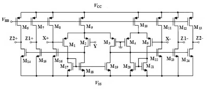
Figure 1. CMOS Implementation of MO-DXCCII [16]
practical realizations of this active element have been successfully explored using commercially available ICs [21]. The CMOS implementation of multi-output dual-X second-generation current conveyor (MO-DXCCII) is shown in Fig. 1. The port relationship of the MO-DXCCII can be characterized as:
I Y
V
V X
I Z 1 +
I Z 2 +
I Z 1
I -
I Z 2 -
- 1
V Y
I X +
I X
(a)
III. PROPOSED CIRCUITS
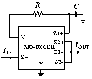
The proposed CM-APFs are shown in Fig. 2. Both the circuits employ a single MO-DXCCII, and the minimal number of passive components (one resistor and one capacitor). Note that the capacitor used is in grounded form, which makes the circuits suitable for integrated circuit implementation. Routine analysis of the circuits of Fig. 2 yields the following current transfer function r s - 1 1
s ( C + C zi - )( R + R X + )
s + 1
v ( C + C Z1 - )( R + R x + ) J
(b)
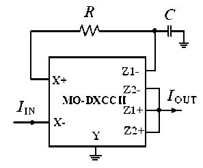
Figure 2. (a) CMAPF-I (b) CMAPF-II
CMAPF-II : IOUT I IN
—
The frequency dependent phase response (Φ) of the filters is given by
ф ( ю ) = —2 tan — 1 ( a CR ) (3)
It is to be noted from (2) that no passive element matching constraints are required for the proposed circuits. The proposed filters exhibit low input and high output impedance, which make them suitable for cascading without requiring additional current buffer circuit. The other salient features of the two proposed circuits are use of single active element and two passive components. The three features are not exhibited together in any of the available work [2-15]. As far as integrated aspect of the new proposed circuits are concerned, the resistor can be replaced by active-MOS resistor with the added advantage of tunability through external voltage [22] and the capacitor can be implemented in MOS technology [23].
-
IV. NON-IDEAL ANALYSIS AND EFFECTS OF
MO-DXCCII PARASITIC
A. Non-ideal Analysis
Taking non-idealities of the MO-DXCCII into account, the port relationships of the voltages and currents modify to
|
I y |
0 |
|
|
V x + |
в 1 |
|
|
V x - |
- в 2 |
|
|
I z 1 + |
= |
0 |
|
I Z 2 + |
0 |
|
|
I z 1 - |
0 |
|
|
I z 2 - _ |
_ 0 |
|
0 |
0 " |
|
|
0 |
0 |
|
|
0 |
0 |
Г V Y 1 |
|
а 1 |
0 |
I X + |
|
а 2 |
0 |
_ I x - _ |
|
0 |
а з |
|
|
0 |
а 4 _ |
Here, α 1 and α 2 are the current transfer gains from X+ terminals to Z1+ and Z2+ terminals, respectively α 3 and α 4 are the current transfer gains from X- terminals to Z1-and Z2- terminals, respectively and β 1 and β 2 are the voltage transfer gains from Y input terminal to X+ and X- terminals, respectively. However, these transfer gains are close to unity up to a very high frequency range (i.e. in GHz) [8].
The proposed circuits are reanalyzed assuming nonideal MO-DXCCII; the modified current transfer functions are found as
TABLE I. SENSITIVITY FIGURES WITH RESPECT TO POLE FREQUENCY ( ω o ) AND GAIN ( H ) FOR THE PROPOSED CIRCUITS OF FIG. 2
|
Circuit |
О Ю о ° а , , а 2 , а з , а 4 , Д , в 2 |
С " о S R , C |
S H а 2 |
SH а 4 |
H u а , , а з , Д , Д 2 , R , C |
|
CMAPF-I |
0 |
-1 |
1 |
0 |
0 |
|
CMAPF-II |
0 |
-1 |
0 |
1 |
0 |
B. Effects of MO-DXCCII Parasitic
Effects of parasitics involved with the used current conveyor are now considered. The various parasitic involved with a typical MO-DXCCII are a small parasitic resistances R X+ and R X- at X+ and X- terminals respectively, parasitic at Y terminal is ( R Y// C Y) and parasitic at Z1+, Z2+, Z1- and Z2- terminals are ( R Z1+ // C Z1+ ), ( R Z2+ // C Z2 ), ( R Z1- // C Z1- ) and ( R Z2- // C Z2- ), respectively [24]. The parasitic model of MO-DXCCII is also shown in Fig. 3. Here, it is assumed that the circuits are restricted to work at frequencies much lower than the corner frequencies of β i (i = 1, 2) and α i (i = 1, 2, 3, 4). But practically it is assumed that the external resistors are much smaller than the parasitic resistors at the Y and Z terminals of MO-DXCCII, i.e. R << R Y or R Z 1 + or R Z 2 + or R Z1- or R Z2- and the external resistors are much greater than the parasitic resistors at the X+ and X- terminals of MO-DXCCII, i.e. R X+ or R X-<< R . A re-analysis of the two circuits given in Fig. 2 yields the following transfer function
CMAPF-I: IOUT I IN
-а 2
а 2 - ^ з - а 4
CR а 2
s +
CR
а, - а - а s +—4----1----2
CMAPF-II: I OUT- = -а 4 ----- CR a 4---
I N s + —
CR
CMAPF-I : I OUT I IN
CMAPF-II : I OUT I IN
Г - 1 )
( C + C zi )( R + R x -)
s +________1________
I ( C + C zi )( R + R x - ) )
r - 1 )
s ( C + C Zi - )( R + R x + )
s + 1
I ( C + C Z1 - )( R + R x + ) J
From (5) and (6), it is to be observed that the nonidealities do affect the filter gain, as it now depends on α 2 and α 4 for the CMAPF-1 and CMAPF–II, respectively but the pole frequency is unaltered by MO-DXCCII nonidealities. The pole-frequency ( ω o ) and gain ( H ) sensitivity for the all-pass filter circuits to the non-idealities as well as external components is analyzed and is tabulated in Table I.
From Table I, it is to be observed as the sensitivities of active and passive components with respect to pole frequency ( ω o) and gain ( H ) are less than or equal to unity in magnitude meaning good sensitivity performance.
From (7) and (8), the parasitic resistances / capacitances get absorbed with the external values. Because the X terminal is connected directly to a resistor so the parasitic resistance at the X terminal of the MO-DXCCII ( R X) can be absorbed as a part of resistance ( R ), where as the parasitic capacitances ( C Z1- or C Z1+) is in shunt with capacitor ( C ). This causes slight deviation in circuit’s parameters, which can be minimized by pre-distorting the designed values to be used in the circuits. It is also seen that the pole-frequency would be in error because of these parasitic. The error is expected to be small for an integrated MO-DXCCII; the actual value to be given in the ‘simulation results’.
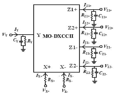
Figure 3. Parasitic Model of MO-DXCCII
TABLE II. 0.35 µ m TSMC CMOS PROCESS PARAMETERS
NMOS:
LEVEL=3 TOX=7.9E-9 NSUB=1E17
GAMMA=0.5827871 PHI=0.7 VTO=0.5445549 DELTA=0
UO=436.256147 ETA=0 THETA=0.1749684 KP=2.055786E-
4 VMAX=8.309444E4 KAPPA=0.2574081 RSH=0.0559398
NFS=1E12 TPG=1 XJ=3E-7 LD=3.162278E-11
WD=7.04672E-8 CGDO=2.82E-10 CGSO=2.82E-10
CGBO=1E-10 CJ=1E-3 PB=0.9758533 MJ=0.3448504
CJSW=3.777852E-10 MJSW=0.3508721
PMOS:
LEVEL =3 TOX = 7.9E-9 NSUB=1E17
GAMMA=0.4083894 PHI=0.7 VTO=-0.7140674 DELTA=0
UO=212.2319801 ETA=9.999762E-4 THETA=0.2020774
KP=6.733755E-5 VMAX=1.181551E5 KAPPA=1.5
RSH=30.0712458 NFS=1E12 TPG=-1 XJ=2E-7
LD=5.000001E-13 WD=1.249872E-7 CGDO=3.09E-10
CGSO=3.09E-10 CGBO=1E-10 CJ=1.419508E-3
PB=0.8152753 MJ=0.5 CJSW=4.813504E-10 MJSW=0.5
-
V. SIMULATION RESULTS
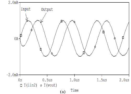
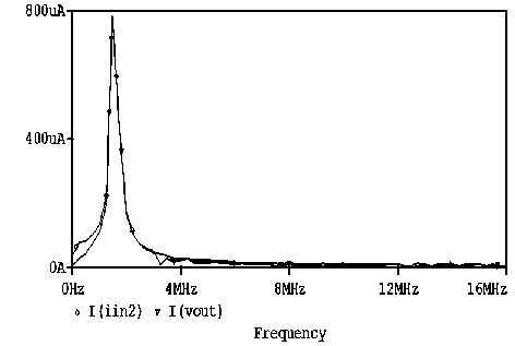
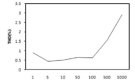
The proposed circuits are verified using the PSPICE simulation program. The MO-DXCCII is realized by the CMOS implementation [16] of Fig. 1 using 0.35 µ m TSMC process parameters (Table II). The aspect ratios of NMOS and PMOS transistors are chosen as in Table III and the supply voltages used were ± 1.8 V and VBB = -1.25 V. The CMAPF-I is designed with C = 100 pF and R = 1 KΩ for a theoretical pole frequency of 1.59 MHz The phase and gain responses for the CMAPF-I are shown plotted in Fig. 4, which shows a constant unity gain and frequency dependent phase. A phase shift of -90 is obtained at the pole frequency and the pole frequency is found to be as 1.51 MHz, which is in consistency with the designed value. Next figure (Fig. 5) shows the time domain input and output waveforms, along with their Fourier spectrum when a sinusoidal input signal of frequency 1.59 MHz is applied at the input terminal of the circuit. The output current is -90 phase shifted with respect to the input, which verifies circuit operation as a phase shifter. In addition, the Lissajous pattern for the circuit as -90 phase shifter is shown plotted in Fig. 6. The variation of the total harmonic distortion (THD) at the output by varying the amplitude of the sinusoidal input current at 1.59 MHz is shown in Fig. 7. It can be seen that the THD value of the filter increases for the input current in excess to 200 µ A (peak to peak). The simulations confirm the proposed circuits and results agree with the theory.
-
VI. INTEGRATION ASPECTS
The integration prospects of the new proposed circuits are considered here. The proposed current-mode first order all-pass filters employ single MO-DXCCII, which can be implemented in CMOS technology [16]. Both the circuits use a single grounded capacitor in its realization, which is suitable for integration. There are techniques to implement the capacitor in MOS technology [23, 25]. The resistor used in the circuits can be replaced by active MOS resistor, available in literature [22], with an added feature of tunability by control voltage. Thus the proposed circuits are suitable for IC implementation.
TABLE III. TRANSISTOR ASPECT RATIOS FOR THE CIRCUIT SHOWN IN FIG. 1 .
|
Transistors |
W( µ m) |
L( µ m) |
|
M 1 -M 2 |
1.4 |
0.7 |
|
M 3 -M 5 |
2.8 |
0.7 |
|
M 17 -M 18 |
2.4 |
0.7 |
|
M 19 -M 21 |
4.8 |
0.7 |
|
M 6 -M 16 , M 22 -M 24 |
9.6 |
0.7 |
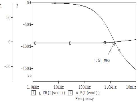
Figure 4. Simulated gain and phase response of CMAPF-I
(b)
Figure 5. (a) Input/output responses (b) Fourier spectrum at 1.59MHz
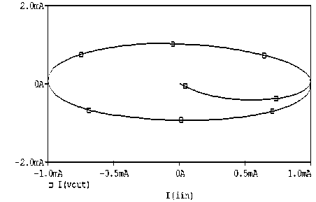
Figure 6. Lissajous pattern showing -90° phase shift at pole frequency
Гш(мА)
Figure 7. THD variation with the sinusoidal input signal at 1.59 MHz
-
VII. CONCLUSION
This paper presents two novel first-order current-mode all-pass filters, employing minimal number of active and passive components i.e. single MO-DXCCII, one resistor and one capacitor. The proposed circuits show low input and high output impedance feature, which is desirable for the CM circuits. Beside this, the circuits employ grounded capacitor which is good for IC implementation in CMOS technology. No passive component matching constraints are required for the proposed filters. The simulation results confirm the workability of the proposed filters.
ACKNOWLEDGMENT
The corresponding authors are grateful to the anonymous referees for their useful comments, which helped to further improve the paper.
References Novel Current-Mode All-Pass Filter with Minimum Component Count
- C. Toumazou, F. Lidjey and D. Haigh, “Analog IC design: the current-mode approach”, Peter Peregrinus, UK, 1990.
- A. Fabre and J. P. Longuemard, “High performance current processing all-pass filters”, International Journal of Electronics, vol. 66, pp. 619–632, 1989.
- M. Higashimura and Y. Fukui, “Realization of current mode all-pass networks using a current conveyor”, IEEE Transactions on Circuits and Systems, vol. 37, pp. 660–661, 1990.
- M. Higashimura, “Current-mode all-pass filter using FTFN with grounded capacitor”, Electronics Letter, vol. 27, pp. 1182–1183, 1991.
- A. M. Soliman, “Theorems relating to port interchange in current-mode CCII circuits”, International Journal of Electronics, vol. 82, pp. 582–604, 1997.
- T. Tsukutani, M. Higashimura, M. Ishida, S. Tsuiki, and Y. Fukui, “A general class of current-mode high-order OTA-C filters”, International Journal of Electronics, vol. 81, pp. 663–669, 1996.
- A. M. Soliman, “New current mode filters using current conveyors”, International Journal of Electronics and Communications (AEÜ), vol. 51, pp. 275-278, 1997.
- A. Toker, S. Ozoguz, O. Cicekoglu and C. Acar, “Current-mode all-pass filters using current differencing buffered amplifier and a new high-Q band-pass filter configuration”, IEEE Transactions on Circuits and Systems II: Analog and Digital Signal Processing, vol. 47, pp. 949–954, 2000.
- S. Maheshwari and I. A. Khan, “Novel first order all-pass sections using a single CCIII”, International Journal of Electronics, vol. 88, pp. 773–778, 2001.
- S. Kilinc and U. Cam, “Current-mode first-order all-pass filter employing single current operational amplifier”, Analog Integrated Circuits and Signal Processing, vol. 41, pp. 47– 53, 2004.
- S. Maheshwari, “New voltage and current-mode APS using current controlled conveyor”, International Journal of Electronics, vol. 91, pp. 735–743, 2004.
- S. Minaei and M. A. Ibrahim, “General configuration for realizing current-mode first order all-pass filter using DVCC”, International Journal of Electronics, vol. 92, pp. 347–356, 2005.
- S. Maheshwari, “A new current-mode current-controlled all-pass section”, Journal of Circuits, Systems and Computers, vol. 16, pp. 181–189, 2007.
- D. Biolek and V. Biolkova, “All-pass filter employing one grounded capacitor and one active element”, Electronics Letter, vol. 45, pp. 807-808, 2009.
- S. Minaei and E. Yuce, “All grounded passive elements current-mode All-pass filter”, Journal of Circuits, Systems and Computers, vol. 18, pp. 31–43, 2009.
- A. Zeki and A. Toker, “The dual-X current conveyor (DXCCII): A new active device for tunable continuous-time filters”, International Journal of Electronics, vol. 89, pp. 913-923, 2002.
- A. Zeki and A. Toker, “DXCCII-based tunable gyrator”, International Journal of Electronics and Communications (AEÜ), vol. 34, pp. 59-62, 2005.
- S. Minaei, “Electronically tunable current-mode universal biquad filter using dual-X current conveyors”, Journal of Circuits, Systems, and Computers, vol. 18, pp. 665–680, 2009.
- S. Minaei and E. Yuce, “A new full-wave rectifier circuit employing single dual-X current conveyor”, International Journal of Electronics, vol. 95, pp. 777–784, 2008.
- S. Maheshwari and B. Chaturvedi, “High-input low-output impedance all-pass filters using one active element”, IET: Circuits Devices and Systems, vol. 6, pp. 103-110, 2012.
- S. Maheshwari and M. S. Ansari, “Catalog of realizations for DXCCII using commercially available ICs and applications”, Radioengineering, vol. 21, pp. 281-289, 2012.
- K. M. Al-Ruwaihi, “A floating voltage controlled linear resistor and its application to active RC filters”, International Journal of Electronics, vol. 92, pp. 483-498, 1997.
- M. Bhusan and R. W. Newcomb, “Grounding of capacitors in integrated circuits”, Electronics Letter, vol. 3, pp. 148–149, 1967.
- S. Minaei and E. Yuce, “Unity/variable-gain voltage-mode/current-mode first-order all-pass filters using single dual-X second-generation current conveyor”, IETE Journal of Research, vol. 56, pp. 305-312, 2010.
- P.E. Allen and D.R. Holberg, “CMOS analog circuit design,” Oxford University Press, 2004, 2nd edn.
