Novel design of 32-bit asynchronous (RISC) microprocessor & its implementation on FPGA
 microprocessor & its implementation on FPGA")
Author: Archana Rani, Naresh Grover
Journal: International Journal of Information Engineering and Electronic Business @ijieeb
Article in issue: 1 vol.10, 2018.
Free access
As the efficiency and power consumption plays an important role in electronic system design, an asynchronous design is used to reduce such challenges faced in synchronous architectures. The asynchronous processors have a number of advantages, especially in SoC (System on chip) including reduced crosstalk between analog and digital circuits, ease of integrating multi-rate circuits, ease of component reuse and less power consumption as well. This paper deals with the novel design and implementation of such type of asynchronous microprocessor by using VHDL on Xilinx ISE tool wherein it has the capability of handling even I-Type, R-Type and Jump instructions with multiplier instruction packet. Moreover, it uses separate memory for instructions and data read-write that can be changed at any time.
Asynchronous design, Processor, VHDL, MIPS, Synthesis & Simulation, Instruction data path, EDA Tools
Short address: https://sciup.org/15016121
IDR: 15016121 | DOI: 10.5815/ijieeb.2018.01.06
Text of the scientific article Novel design of 32-bit asynchronous (RISC) microprocessor & its implementation on FPGA
Published Online January 2018 in MECS
Now- a- days computers are evolving using RISC (Reduced Instruction Set Computer) Architecture replacing stack architecture with the intention to displace the hypothetical, emulated computer by a real one. Instruction Set Architecture (ISA) design is the concept of CISC (Complex Instruction Set Computer) that emphasize more on each instruction using a wide range of addressing modes and number of operands in various locations in its Instruction Set. This leads to execution time to vary as instructions are not of fixed length, hence demanding a very complex Control Unit, which occupies a large area on chip. While on the other side, the RISC Processor has less number of Instructions. The fixed instruction length with more general purpose registers to support load-store architecture and simplified addressing modes. This makes individual instruction to execute faster in order to achieve a net gain in performance and an overall simpler design with less silicon consumption.
The choice of an RISC has become more obvious with the increase in size and complexity of modern processors and software. The hardware designer has a substantial amount of freedom for design by making use of FPGA being much more aware of availability of resources and of its limitations than the software developer.
Before commencing the design of an asynchronous processor we have to first focus on the architecture of Asynchronous processor as well as the various steps involved in such designs in terms of the program cycle. This paper presents processor architecture design, its implementation followed by processor instruction set, data path flow for fetching unit, Register type, I-type and load /store type instruction flow. Thereafter this paper illustrates control unit design of processor that shows the controlling of signals for different units in processor design. Further, a complete internal structure is shown followed by features of novel processor architecture. In the end, results have been shown using implementation windows. The complete design has been written using VHDL and then simulated and synthesized by XILINX ISE tool.
-
A. Processor Architecture
The asynchronous processor internal operation is segmented into five pipeline stages and in each of them the operations of the tasks will be performed in the normal cycle of an instruction, i.e. search of the instruction (identified with the IF block), decoding of The instruction (identified with the ID block), execution of the operation (identified with the EX block), memory access (identified with the MEM block) and storage of the operation result (identified with the WB block) [24].
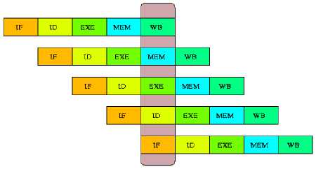
Fig.1. Processing Stages
-
B. Instruction Set Format
The Asynchronous Processor has fixed width instructions (32- bit). There are 3 instruction types: I-type (Immediate), R-type (Register), J-type (Jump). Fig. 2 shows the format of I-type and R-type instructions. [23]
|
Opcode |
RS |
RT |
Address/immediate |
||||
|
6 |
5 5 16 Fig.2. (a) I-Type Instruction |
||||||
|
Opcode |
RS |
RT |
RD J |
Shift |
Function |
||
6 5 5 5 5 6
Fig.2(b). R-Type Instruction
MIPS ( Microprocessor without Interlocked Pipeline Stages) are load/store architecture, meaning that all operations are performed on values found in local registers. The main memory is only accessed through load (copy value from memory to local register) and store (copy value from local register to memory) instructions.
The fields in the MIPS instructions are the followings:
-
• OPCODE – 6-bit operation code
-
• RS – 5- bit specifier for source register
-
• RT – 5- bit specifier for target register
-
• RD – 5- bit specifier for destination register
-
• Address/immediate – 16-bit signed immediate
used for logical and arithmetic operands, load/store address offsets
-
• Shift – 5-bit shift amount
-
• Function – 6-bit code used to specify functions
-
II. Instruction Implementation
-
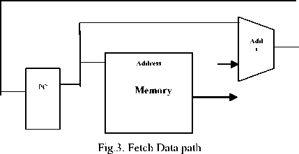
A. Fetch Data path Flow
Figure 3 shows the Fetching of an instruction from memory. The PC (Program Counter) always indicates the location of the instruction to execute. The location is basically an Internal ROM where all instruction (to be executed) are stored at different locations. Once the PC fetches an instruction from its current value, the PC address automatically advances by 4. The order of the PC can be changed by the occurrence of the instruction stored in the memory block.
-
B. Register Type Data path Flow
The register type instruction(s) is the instruction involved with the data to be communicated to and fro from the internal (general purpose registers)/external registers (RAM). After being fetched, the instruction is bifurcated into fields i.e. Opcode (Store/shift/Add etc.), source and destination register location/data with some controlling signals named register write or read registers. Then the data or value of the specified register location will propagate through ALU for different operations to be performed.
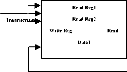
Fig.4. R-Type Data path Flow
ALU Operation
-
C. Load/Store Datapath Flow
Figure 5 shows the data path flow for the immediate instructions to load and store at various location, these locations may be any general purpose or any memory locations that can be addressed randomly.
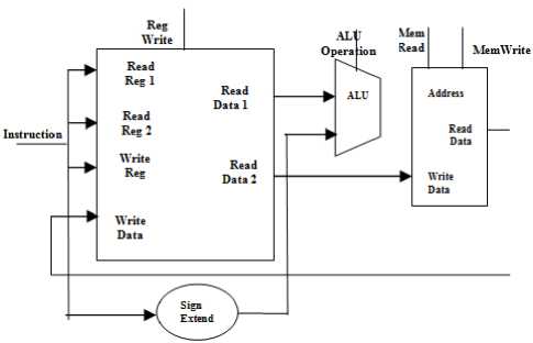
Fig.5. Load/Store Datapath Flow
D. Multiple Instruction Datapath Flow
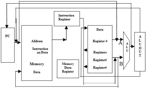
Fig.6. processing paths for all instructions
Table 1. Action for all instructions
|
Step |
R-Type Actions |
Memory reference Actions |
|
Fetch |
IR= Memory[PC] PC= PC+4 |
|
|
Decode |
A= Reg[IR(25-21)] B= Reg[IR(20-16)] |
|
|
Execution |
ALUout= A op B |
ALUOut = A= Sign_extend(IR[15-0]) |
|
Memory |
Reg[IR(15-11)]= ALUOut |
Load:MDR= Memory{ALUOut} Or Store: Memory{ALUOut}=B |
|
Write Back |
Load Reg[IR(20-16)]=MDR |
|
Table 1 shows all actions necessary for the execution of an instruction (of any type) during each stage(s). To differentiate the type of instruction we had design one control unit which takes care of overall operation execution cycle.
-
E. Control Unit Design
The design of control unit has been divided into various states through which it is going to generate the control signals for other components in the design, based on the current state and on the instruction code. Following are the control signals:
MemRead : if 1, read from memory;
MemWrite : if 1, write to memory;
RegDst: if 1, the destination number for the Write register comes from the Rd field; if 0, it comes from Rt field;
RegWrite: if 1, the general-purpose register selected by the Write register number is written with the value of the Write data input;
AluSrcA: (ALU Source A) if 1, the operand is A register; if 0, the operand is PC;
MemtoReg: if 1, it comes from Memory data register (MDR) and if 0, the value fed to the register file Write data input comes from ALUOut;
IRWrite: if 1, write instruction is performed in IR;
PCWrite: if 1, update the PC;
The control unit is basically the part of our 32-bit asynchronous processor. The complete designs of processor architecture have been distributed into small units. Proposed design has various sub modules which are basically named as ALU control unit, RAM / ROM blocks, PC unit, Shift, Add, Multiplier units for various arithmetic and logical instruction. In the end, interfacing module for all the sub units is designed. As each unit has their own significance, the major role played by the control unit is to command/control the overall operation. Hence more emphasis has been given to this unit.
-
F. Processor Architecture
This section deals with the complete internal structure of our 32-bit Asynchronous Processor. All the various stage(s) required for an instruction processing is been identified by the call out(s) box(es). Figure 7 shows the internal architecture of Asynchronous processor, In this processor, fetching the instruction pointed by the Program counter goes to the next unit called decoder which generates the different values of the memory location, as per the instruction fetched from the previous unit. During this control unit has been designed in order to synchronize the various other units such as ALU, data memory or general purpose registers to properly execute the desired instruction. There are other units named as ALU, data memory, and some multiplexers to complete the execution cycle. The entire major units have been discussed previously.
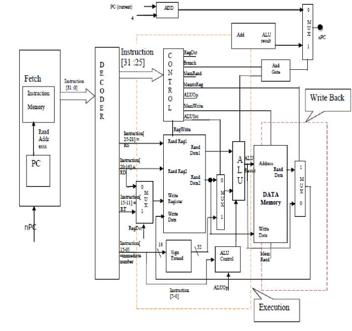
Fig.7. Internal Structure of the Processor
-
III. Features of Novel Processor
The 32-bit asynchronous processor has the capability of handling all types of instructions i.e. I-Type, R-Type, Jump Instructions and also multiply instructions packet. The multiplied result is stored until is needed irrespective of other instructions follows.
The proposed processor is using separate memory for instructions and Data. The capacity of instruction memory i.e. ROM is of 8192*32 in which 8192 are representing the locations where instructions are to be stored with 32-bit data. The structures of instructions are as per ISA (instruction set Architecture). For all stages, there is only one clock cycle needed, while the data memory has the capacity of 64K. Both memories are functioning in falling pulse. The other pulses are used for developing the necessary functions just like pipelining in order to make our processor core faster and much flexible.
All I-type instructions are part decoded in the first stage and all R-type instructions are part decoded in ALU control unit. This reduces the complexity in main control unit. The complete processor core is designed in Xilinx ISE 14.x tool.
-
IV. Design Implementation
The complete processor has been implemented on the Xilinx ISE tool. All the coding have been done in VHDL and simulated or verified by the XILINX ISIM. The following windows come from Xilinx simulator for various instructions Stored in Instruction memory. Figure 8 shows the project settings i.e. the target family Virtex-6, with device name XC6Vlx240T.
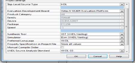
Fig.8. Project setting window in Xilinx ISE
-
A. Instruction Memory Window
Figure 9 shows the various instructions written into internal memory. From which PC fetches the instruction to be executed. In figure 10 the table shows the complete structure of the mnemonics for asynchronous processor instruction. The order of instruction execution can be changed as per the designers or consumer requirement. Although once written in Instruction memory the order of the execution of instruction will be as per the order of the mnemonics appears. The Instruction memory is also known as code memory /ROM where all the instructions are going to be stored permanently. The overall execution of any instruction is always been started by the code/instruction memory. In the below figure we have shown some instruction mnemonics although we can store /provide various instruction up to 32 KB i.e. 8192 memory location available and on each location one can store up to 32 bit of data. Also, we are having 32*32 register for temporary storage of the output or any general purpose work. This is shown in figure 10.
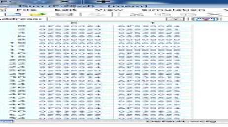
Fig.9. Instruction Memory inferred in Xilinx ISE Tool.
|
Memor |
Instruction |
Instruction Field |
|||||
|
y Addr |
OP - opc ode |
RS Sour ce regi |
RT |
R T d |
Sha mt |
Fun c |
|
|
00 |
Sw $s1,100($s2 ) |
101 011 |
1110 0 |
01001 |
000000000110010 0 |
||
|
04 |
Lw $s1,100($s2 ) |
100 011 |
1110 0 |
01001 |
000000000110010 0 |
||
RS -Source register, RT -Destination register, RTD -Destination register, Shamt -Shift amount, Func - Function
Fig.10. Mnemonics of Instruction
-
B. Register Bank Window
Figure 11 shows the internal register bank arrangements of the designed processor. By default, all the values in registers are (in 32-bit Binary) "0000000000000000000000000000". We kept some values during the operation of addition and subtraction so that we never get zero as an output. There are thirty-two, 32-Bit registers to temporary hold the data. These registers can be used in any type of addressing modes i.e. Immediate, Register Direct or Indirect addressing modes. The values in the corresponding registers will automatically update once the instruction will be fetched and executed.
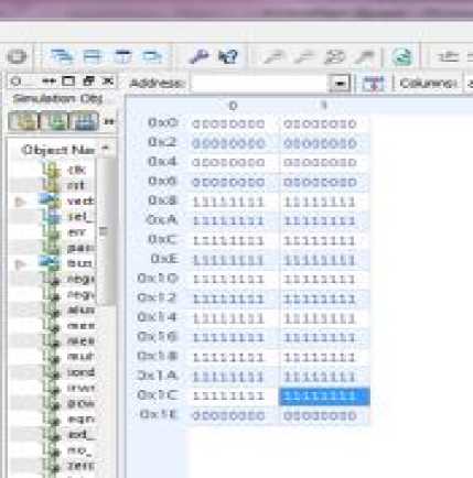
Fig.11. Register Bank inferred in Xilinx ISE tool
-
V. Simulation Results
The simulation is carried out on Xilinx ISIM tool and results are shown in this section. Figure 12 shows the result with initial conditions i.e. Rst='0'. So that the processor comes into its initial state with the initial values in all types of the registers.
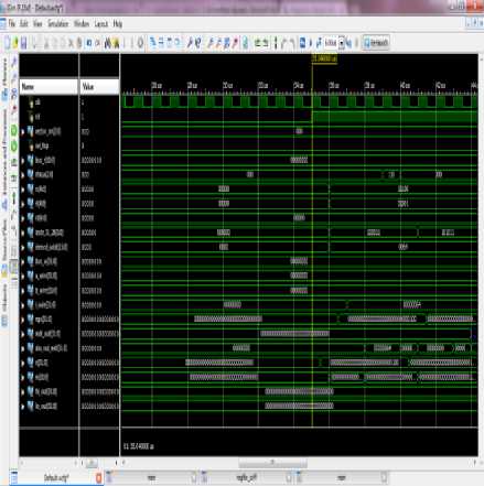
Fig.12. Simulation with initial Condition i.e. Rst=’0’.
Figure 13 & 14 shows the simulation result for loading of a number from memory to a register. The instruction for this is 8F890064 (1000111110001001 0000000001100100 b), where 100011b is the Opcode, 11100 is source location, 01001b is Destination register location and rest is the immediate address from where data to be read. The instruction works as:
Rt = mem [rs(data)+64h] where rt= 1001b or 9(h/d),
Rs =11100b or 1ch or 28d in register bank and having zero value. So the resultant address from where data to be fetched would be 64h+0h= 64h. The content of this 64h will be loaded into the 9 register in register bank.
Hex code: 8F890064, LW $s1, 100($s2) Load word
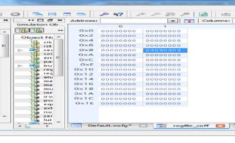
Fig.13. Register bank updated Value
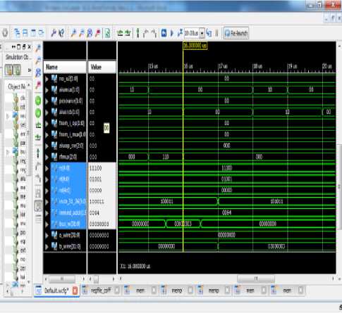
Fig.14. Load data from memory
Hex Code: AF890060 SW $s1, 96($s2) Store word
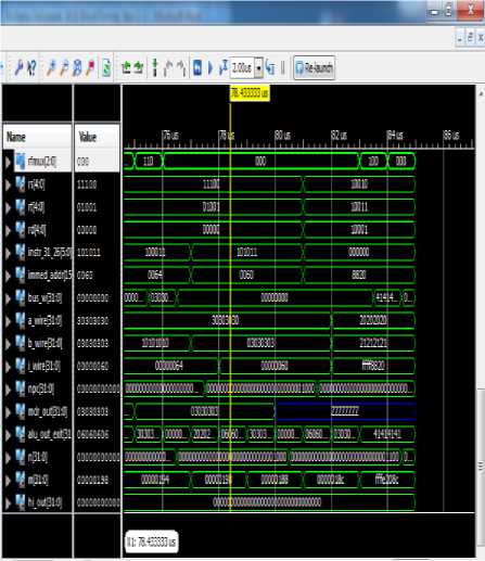
Fig.15. Storing of an immediate number
Figure 15, shows the simulation for the instruction to store some number from register to memory location. “AF890060”, is the mnemonics for this instruction. This will perform the storing the number from the specified location i.e. 1001 (9) to the address hold by the rs and constant value. The yellow marker shows this happening in the simulation cycle.
mem [rs+60h]= rt where rt= 1001b or 9(h/d),
Rs =11100b or 1ch or 28d in register bank and having zero value. Since Rt holds the value 30303030H, now this value is going to be written in the memory location.
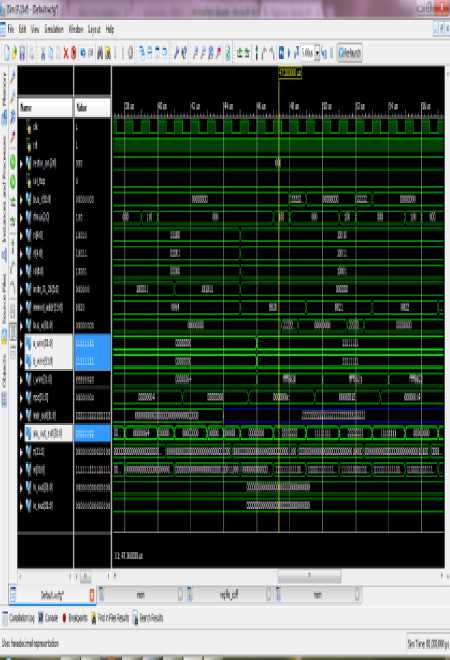
Fig.16. Addition of values from register bank
Figure 16 shows the simulation output of the Addition operation of the values stored into internal register bank. The opcode for this instruction is 2538820. The register location(s) are marked by blue color in the simulation diagram.
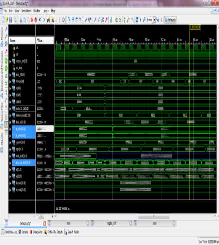
Fig.17. Subtraction of values from register Bank
The above figure shows the complete summary of our implemented design, which carries the information(s) about the number of resources i.e. inferred gates/FFs/dedicated LUTs, has been used by the implemented designed. Through this information, we can also put some extra efforts in the direction of optimizing our design for the best possible result.
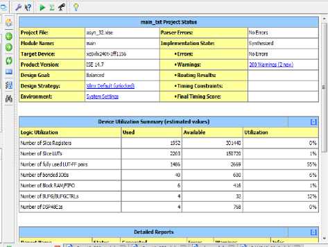
Fig.18. Device Utilization Summary
-
A. Overall processor Simulation Results
Figure(s) 19 and 20 are showing the overall processor results. While initializing the processor with rst =’1’. Our processor starts fetching the instruction from ROM/ Instruction memory which contains the Store, Load word and Addition and Subtraction operation. Due to large simulation signals we had divided our simulation windows in two halves. The first half i.e. figure 19 shows the signals like clk, rst, Aluop, Alusw, AlusrcA, IRwrite etc. These signals are basically coming from the control Unit to bind the overall instruction execution. For simplicity we had taken out Bus_r(31:0) for the final output. Although we can verify these data into the internal memory location(s) or Register Memory Window.
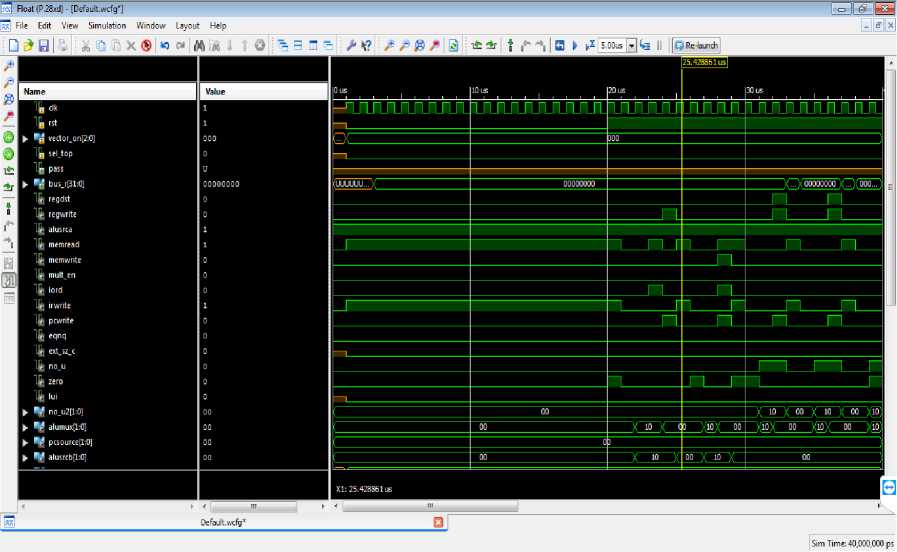
Fig.19. Overall Processor Simulation result (1)
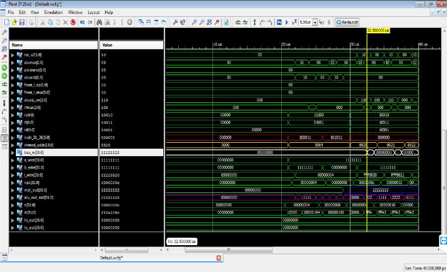
Fig.20. Overall Processor Simulation result (2)
The instr(31:26) signal shows the process of opcode fetching from Instruction memory, it starts from 8F, i.e.opcode for the loading of data into the memory, the next is AF for storing the data from memory, then 02 for Addition and so on. On every clock pulse the new instruction will be fetched and update automatically the instr(31:26) signal. This signal in simulation waveform is highlighted by the color RED.
The immed_addr(15:0) signal shows the immediate value for the use of ALU operations. This signal is highlighted by Yellow color in simulation waveform. The intermediate Bus (31:0) is showing the data output from the ALU after completion of any instruction. This is highlighted by the color white. At last the output from A showing by ALU_OUT(31:0) highlighted by the color Purple.
-
VI. Conclusion
The 32-bit fully functional asynchronous processor has been designed using VHDL. A fully asynchronous processor has been implemented that is comprised of five stages. The work can be potentially improved by reducing I and R-type instructions. The functional simulation shows that proposed processor executes all the various instructions efficiently. The proposed design being an open core is more advantageous as compared to the existing commercial microprocessor for better understanding of internals of the asynchronous microprocessor.
Future Scope
References Novel design of 32-bit asynchronous (RISC) microprocessor & its implementation on FPGA
- Afreen Tashfia., Minhaz. Uddin Md Ikram, Aqib. AI Azad, and Iqbalur Rahman Rokon," Efficient FPGA Implementation of Double Precision Floating Point Unit Using Verilog HDL", International Conference on Innovations in Electrical and Electronics Engineering (ICIEE'20 12), October 2012, Dubai (UAE).
- Aneesh, R.; Jeju, K. "Design of FPGA based 8-bit RISC controller IP core using VHDL", India Conference (INDICON), 2012 Annual IEEE, On page(s): 427 – 432
- Anjana R & Krunal Gandhi, “VHDL Implementation of a MIPS RISC Processor”, August 2012, International Journal of Advanced Research in Computer Science and Software Engineering, pp 83-88
- Bhosle Preetam, Hari Krishna Moorthy, "FPGA Implementation of Low Power Pipelined 32-bit RISC Processor", Proceedings of International Journal of Innovative Technology and Exploring Engineering (IJITEE), ISSN: 2278-3075, Vol-I, Issue-3, August 2012.
- Ferdous, T. "Design and FPGA-based implementation of a high-performance 32-bit DSP processor", Computer and Information Technology (ICCIT), 2012 15th International Conference, on page(s): 484 – 489
- Grover Naresh, Dr. M.K. Soni, “Reduction of Power Consumption in FPGAs - An Overview”, I.J. Information Engineering and Electronic Business, 2012, 5, 50-69
- Grover Naresh, Dr. M.K. Soni, “Design of FPGA based 32-bit Floating Point Arithmetic Unit and verification of its VHDL code using MATLAB”, I.J. Information Engineering and Electronic Business, 2014, 1, 1-14
- Indu, Arun Kumar, “Design of Low Power Pipelined RISC Processor”, International Journal of Advanced Research in Electrical & electronics & instrumentation Engineering, vol.2, no.3, pp.3747-3756, August 2013.
- Kathuria Jagrit, M. Ayoubkhan, Arti Noor, "A Review of Clock Gating Techniques", MIT International Journal of Electronics and Communication Engineering vol 1, no. 2, August 2011.
- Kumar B. Rajesh, Ravisaketh, and Santha Kumar, 2014, "Implementation of A 16-bit RISC Processor for Convolution Application", Research India publications, pp 441-446.
- Li Li and Ken Choi “SeSCG: Selective Sequential Clock Gating for Ultra - low-Power Multimedia Mobile Processor Design,” IEEE EIT Conference, May 2010.
- MD. Shabeena Begum, M.Kishore Kumar, "FPGA based implementation of 32-bit RISC processor", International Journal of Engineering Research and Applications (IJERA), pp 1148-1151
- Mohammad Imran, Ramananjaneyulu, "FPGA Implementation of a 64-bit RISC Processor Using VHDL", Proceedings of International Journal of Reconfigurable and Embedded Systems(IJRES), ISSN:2089-4864, Vol-l, No.2, July 2012.
- Purna Addanki Ramesh, Ch.Pradeep,"FPGA Based Implementation of Double Precision Floating point Adder/Subtractor Using Verilog", Proceedings of International Journal of Emerging Technology and Advanced EngineeringISSN-2250-2459, Vol-2, issue 7, July 2012.
- Ramkumar B. and Harish M Kittur "low power and Area- Efficient Carry Select Adder" IEEE Transactions on Very Large Scale Integration (VLSI) Systems, vol. 20, no.2, 2012, pp. 371-75.
- Ravindra J., T.Anuradha,"Design of Low Power RISC Processor by Applying Clock gating Technique", International Journal of Engineering Research and Applications, ISSN2248-9622, Vol-2, Issue-3, May-Jun- 2012
- Sakthikumaran Samiappa , S. Salivahanan, V.S,kanchan. Bhaskaran, "16 bit RISC Processor Design For Convolution Application " IEEE - International. Conference on Recent Trends in Information technology pp.394 - 397, June 2011.
- Sidheeq Aboobacker.V.M,"Four Stage Pipelined 16-bit RISC on Xilinx Spartan 3AN FPGA", Proceedings of International Journal of Computer Applications, ISNN: 0975-888, Vol-48, June 2012.
- Tina G Galani, Riya Saini and R.D.Daruwala,"Design and Implementation of 32-bit RISC Processor using Xilinx", international Journal of Emerging Trends in Electrical and Electronics(IJETEE), ISNN:2320-9569, Vol- 5, issue I, July-20 13.
- Trivedi Priyanka, Rajan Prasad Tripathi "low Power pipelined RISC processor: A Review," IJSRD vol.2, no.4, pp. 526-528, July 2014.
- Uma R., " Design and Performance analysis of 8 bit RISC Processor Using Xilinx Tool", International Journal of Engineering Research and Application, vol.2, no.2, pp. 53-58, April 2012.
- Ritpurkar Sagar P., Prof. Mangesh N. Thakare, Prof. Girish D. Korde," Review on 32-bit MIPS RISC Processor using VHDL", IOSR Journal of Electrical and Electronics Engineering (IOSR-JEEE), PP 46-50
- Xiao Li, Longwei Ji, Bo Shen, Wenhong Li, Qianling Zhang, "VLSI implementation of a High-performance 32-bit RISC Microprocessor", Communications, Circuits and Systems and West Sino Expositions, IEEE 2002 International Conference on, Volume 2, 2002,pp.1458 – 1461.
- Wikipedia https://en.wikipedia.org/wiki/Asynchronous_circuit http://www.alteraforum.com/forum/forum.php
- MIPS Instruction set architecture https://classes.soe.ucsc.edu/cmpe110/Spring11/lectures/04_MIPS_ISA%20.pdf
- MIPS Architecture https://en.wikipedia.org/wiki/MIPS_architecture
