On chip optical neural networks based on mmi microring resonators for image classification

Author: Bui T.T., Le D.T., Nguyen T.H.L., Le T.T.
Journal: Компьютерная оптика @computer-optics
Section: Дифракционная оптика, оптические технологии
Article in issue: 4 т.47, 2023.
Free access
We propose a new on-chip optical neural network (OONN) based on multimode interference-microring resonators (MMI-RRs). The suggested structure eliminates the need for wavelength division multiplexers (WDM) to create an optical neuron on a single chip. New microring resonator structure based on 4×4 MMI coupler with a size of 24µm × 2900 µm is used for the basic elements of the computation matrix, as a result a higher bandwidth and free spectral range (FSR) can be achieved. The Si3N4 platform along with the graphene sheet is designed to modulate the signals and weights of the neural networks at a very high speed. The Si3N4 can provide wide range of operating wavelengths and can work directly with the wavelengths of color images. The structure's benefits include rapid computing speed, little loss, and the ability to handle both positive and negative values. The OONN has been applied to the MNIST dataset with a speed faster than 2.8 to 14x times compared with the conventional GPU methods.
All-optical dot product, image processing, multimode interference coupler, optical convolutional neural networks, optical signal processing, microring resonators, silicon photonics
Short address: https://sciup.org/140301850
IDR: 140301850 | DOI: 10.18287/2412-6179-CO-1211
Text of the scientific article On chip optical neural networks based on mmi microring resonators for image classification
In recent years, to deal with the growing demand for faster computation, computing processors such as central processing units (CPUs), graphics processing units (GPUs) and tensor processing units (TPUs) have been extensively developed [1]. However, Moore’s law in electronics is approaching the limit and slowing down the speed of data-processing-related improvements. Light has been recently established as a communication medium for telecommunications and data centers, but it has not been widely utilized in information processing, computing and optical neural networks [2, 3]. The neural networks implemented in the optical domain can provide particular advantages such as high-throughput, power-efficient, and low-latency computing performance [4].
In the literature, there are some optical methods for the dot product or matrix vector multiplication implementation and optical neural networks, such as microring resonators (MRRs), microdisk resonators (MDRs), Bragg gratings or Mach–Zehnder interferometers (MZIs) [5, 6]. Additionally, the two modulation methods for signals and weights – one based on the thermo-optic effect and the other on the plasma dispersion effect – were primarily used in the proposed work. In these structures, microring resonators are basic elements for weight banks [7]. The main disadvantage of this structure is difficult for the on-chip connection and the requirement of using an optical directional coupler [8]. Therefore, this structure is very sensitive to the fabrication and requires a complex control
architecture to achieve extract the desired transmissions. In order to achieve the desired factor of the kernel, it requires complex control systems [9]. Therefore, in this study, we propose microring resonators based on a 4×4 MMI coupler for implementing modulators and weight banks without using directional couplers. The new microring resonator based on 4×4 MMI coupler can provide a high free spectral range (FSR) compared with others in the literature due to its special architecture. As a result, the proposed structure can work with a higher bandwidth and the matrix dimension of the kernel used in neural network based on this basic element can be increased. In addition, by using the new microring resonator based on 4×4 MMI for optical neuron weight banks, the extract coupling ratios which control the precisely working principle of the device can be obtained. Our proposed structure also does not need to require the WDM as required by the previous research [10].
With the development of silicon photonics, the silicon photonic-based architecture has been shown to perform multiply-accumulate operations at frequencies up to five times faster than conventional electronics [11]. The method employs a bank of tunable silicon MRRs that recreate on-chip synaptic weights. However, the graphene material is a particular attraction to create high-speed optical devices. The state-of-the-art tuning speed of graphene microring is at 130 GHz due to the refractive index of the graphene layer sheet changed by applied voltage into the graphene sheet [12]. On the other hand, the electronic processors have their clock rate limit at around 4–5 GHz as they reach the thermal dissipation limit. Therefore, there is a motivation to explore how photonics could be used to perform convolutions and matrix multiplication. The optical implementation of convolutional neural networks with fast operation speed and high energy efficiency is appealing owing to its outstanding capability of feature extraction and high-speed data processing. Convolutional neural networks, in particular, spend over 80% of their processing time on MVM-based convolutional processing, which is a computationally costly operation in electronics. As a result, hardware and MVM operations can be matched to accelerate convolutional neural networks [13].
In this study, the optical neuron performing matrixvector multiplication with a new compact structure without using WDM is proposed. Our structures use the graphene, so it can provide a higher speed up to 2.8 to 14× times compared with GPUs convolution. The resonance wavelength can be achieved accurately. The material Si3N4 platform is used; it is suitable for the existing CMOS technology, and has little loss. In addition, the proposed structure uses special 4×4 MMI based microring resonators for weight banks, so it can provide a large fabrication tolerance of ±2 µm in the length. Such high fabrication tolerance can help the building of a fully-connected network based on the proposed OMMM for the novel optical implementation of convolutional neural networks in the future. The proposed OONN is applied to perform highly efficient CNNs for image classification and recognition. Our OONN is put to the test using the MNIST hand-writing dataset. The neural network is trained using two layers, and after that, the factors are added to the OONN. For the implementation of the negative values, we specifically use the add-drop filters based on MMI resonators [14]. As a result, the neural networks can be extended in the future.
Theory of all-optical neural networks based on MMI microring resonator structures
Figure 1 shows the proposed OONN with optical neuron based on MMI resonators without the WDMs. The convolutional neural network (CNN) consists of some elements, such as convolutional, nonlinear, pooling and fully connected layers. The kernel of the proposed structure of Fig. 1 with 4 weight factors, for example, can be expressed by
У1 = Х1Wn + x 2 W12 + x 3 W13 + x4 W14 , (1) where xi (i = 1,2, 3,4) is the element of the window in the input image and w1i (i = 1, 2, 3,4) is an element of the kernel filter. The filter scans the input image two-dimensionally and product-sums are computed at every spatial position. As illustrated in Fig. 1, our proposed architecture comprises four sets of cascaded MMI microring resonators (MRRs) and a 1×4 multimode interference (MMI) coupler with an only single-mode light source. Input signals xi and filter factors w1i are the signals that are applied to the first and second MRRs, re- spectively, after being converted to the driving voltage signals. Each of the two MRMs modulates the continuous wave (CW) light from the light source and an optical output from the cascaded MRMs corresponding to a product of xi and w1i.
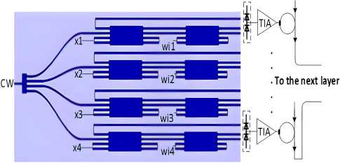
Fig. 1. New Architecture based on 4×4 MMI microring resonators for the dot product implementation
The proposed OONN is trained by changing the values of the kernels, analogous to how feed-forward neural networks are trained by changing the weighted connections. The estimated kernel and weight values are required in the testing stage. The input signal is encoded using the first column array of the MMI-based microring resonators and the weight factors or the kernel filter needs no modification because of the unchangeable kernel. Using only this structure, any filter can be created by changing the weight factor through the control of the resonance wavelength as presented in the next section.
A new optical microring resonator based on only one multimode waveguide with four ports is shown in Fig. 2. We use Si3N4 waveguide with a width of 1600 nm and height of 180 nm for input and output waveguides. For a multimode waveguide, we use a wider width of W MMI =24 ц m. In this structure, we use feedback waveguides for ring waveguides and form the add-drop microring resonator. The drop and through ports T p and T d are shown in Fig. 2. In a multimode waveguide, the information of the image position in the x direction and phases of the output images is very important. To design output waveguides that can capture the optical output, we must understand where multi-images occur. Furthermore, for devices like MMI switches, the phase information of the spot images or output images is crucial. It can be shown that the field in the multimode region will be of the form [15]:
1 N - 1
f ( x , L mmi ) = -7= £ f n ( x - X p ) exp( - j ф p ), V N p = 0
where xp = b (2 p - N) WNML, Фp = b (N - p) N, fin (x) describes the field profile at the input of the multimode region, xp and фp describe the positions and phases of N self-images at that output of the multimode waveguide respectively, p denotes the output image number and b describes a multiple of the imaging length. For the short device, we choose b = 1.
Ini
Phase shifter^e (Graphene) L^
4x4 MMI Resonator
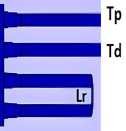
Fig. 2. Microring resonator based on only one multimode waveguide structure
Consider a 4×4 multimode waveguide with the length of L = L mmi = (3 L л )/2, where L к = л /( P 0 - P 1) is the beat length of the MMI, p 0 , P 1 are the propagation constants of the fundamental and first order modes supported by the multimode waveguide with a width of W MMI . The phases associated with the images from input i to output j can be presented by
% -- 2( - 1) ' + j +
+77 i ' + j - i 2 - j 2 + ( - 1) ' + j (2ij - i - j + 1 16 2
matical operations such as matrix–vector multiplication and matrix–matrix multiplication are usually performed in the real number domain in practice. In order to extend the matrix operation to the full real number domain, the final results need to be obtained via the differential processing between the power values of the drop port and the through port; in this way, the transmission matrix and final output vector are both able to contain the negative domain. The output intensities at the two ports of the output in the balanced detections can be expressed by
I out 1 _a sin2( ^) I in , (6)
I u 2 _a cos2(^) Ite , (7)
where a is the loss factor. As a result the intensity after the balanced photo-detector is A I = I out 2 - I out 1 = a l n |cos Аф |, Аф is the phase difference in the two arms. Therefore, both negative and positive values can be achieved using this proposed method. The output signals at the drop port can be expressed by:
Y d _ ( y d1 , y d 2 ,■■■, y dN ) T _
We showed that the characteristics of an MMI device can be described by a transfer matrix [16]. This transfer matrix is a very helpful tool for analysing cascaded MMI structures. The phase ф^ associated with imaging an input i to an output j in an MMI coupler. These phases ф^ form a matrix S 4×4 , with representing the row number, and j representing the column number. A single 4×4 MMI coupler at a length of L MMI = (3 L л ) / 2.
The light propagation through the resonator is characterized by a round trip transmission E in ,3 = a exp ( j 9 ) E n ,4 , where
2 л
9 = ne ffLR
К
w 11
= WX _
w 21
w N 1
W 12
W 22
W N 2
W 1 N
W 2 N
x 1
x 2
x N
The output signal at the through ports can be expressed by
Y t _ ( У t1 , y t 2 ,..., У ® ) T _
1 - Wn
1 - W 21
w N 1
1 - W 12
1 - W 22
...
1 - W n 2
1 - W 1N
1 - W 2 N
...
1 - W nn
x 1
x 2
...
x N
is the round trip phase, a is the loss factor, n ef is the effective refractive index of the SOI single mode waveguide and L R is the ring resonator circumference. We connect the through and drop ports into the balanced photodiode. The normalized transmitted powers at the can be calculated by
T _ 0.25a _ I d 1 -a cos(^) + (0.5a)2 out 1,
T _ 0.5a2 - acos(^) + 0.5 _ i t 1 -a cos(^) + (0.5a)2 out2
The add-drop microring structure is widely applied in on-chip optical computing owing to the capability of difference processing. Since the power value is nonnegative, early work only utilized the through port, then the transmission matrix and the output vector are nonnegative, thus the matrix operation is limited in the nonnegative number domain. However, fundamental mathe-
Simulation results and discussions
In order to obtain the desired factor xi and wij, we use the graphene sheet integrated with Si3N4 waveguide. Graphene can be incorporated into Si3N4 core waveguide to implement graphene silicon nitride waveguide (GSW). The length of the graphene waveguide is L arm . The crosssection view of the graphene silicon waeguide is shown in Fig. 3 a .
The GSW has a monolayer graphene sheet of 340 nm on top of a Si3N4 waveguide, separated from it by a thin Al2O3 layer. Graphene, Al2O3 and silicon together formed a capacitor structure, which was the basic block of the graphene modulator and phase shifter [17]. The presence of the graphene layer changes the propagation characteristics of the guided modes and these can be controlled and reconfigured by changing the chemical potential by means of applying a suitable voltage Vg. The real parts of the refractive index of graphene with different chemical potentials are shown in Fig. 4. Owing to its band structure, which offers both intra-band and interband transitions, graphene exhibits optical properties. Hence, the material conductivity expressed by both types of transitions [18]:
phene sheet. It is because it will change the value of the chemical potential:
IЦ c (V g )| — h Vf ^ «h< V g - V » )|
° ( to ) — O int ra ( to ) + Om t er ( to ).
Where о int ra ( to )and a int er ( to ) are the intraband and interband conductivities, which can be calculated by the Kubo’s theory:
Where V 0 is the offset voltage from zero caused by natural doping. Fig. 4 b and 4 c present the effective index of the Si3N4 waveguide for real and imaginary parts depending on the chemical potential.
-^- + 2ln( e -(ц c / k B T ) + 1) k B T
ie 2 ° int ra (to) — ~ ._ .
uh ( to+ 1 2 Г )
|
ie 2 °-"(to ) —- 4 ^ h ln |
2 |
ц c |
- ( to- 2 i r ) h' |
|
2 |
Ц c |
+ ( to- 2 i r ) h У |
, (11)
Where e is the electron charge, Й is the angular Planck constant, k B is the Boltzman constant, T is the temperature, ц c is the Fermi level or Chemical potential; Г — ( eVF^ )( цц c ) is the electron collision rate, ц is electron mobility, V F is the Fermi velocity in graphene. The dielectric constant of a graphene layer can be calculated by [19, 20]:
e g ( to ) — 1 +
i o(to) toE0A'
The refractive index of the graphene layer sheet can be changed by providing applied voltage V g to the gra-
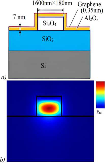
Fig. 3. (a) Waveguide graphene structure, (b) mode profile
a)
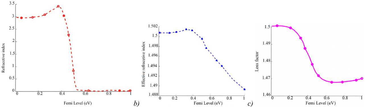
Fig. 4. Effective refractive index of the GSW waveguide
The normalized powers at the through and drop ports of the MMI-based resonator are shown in Fig. 5 a . The difference power between the two ports is in the range of (–1, +1) for negative values of the kernel filters. In this simulation, the chemical potential at the graphene is 0.6 eV . By controlling the chemical potential, we can control the transmission. As a result, the desired values of the kernel factor and input image can be obtained. Fig. 5 b presents the normalized transmissions at through, drop and difference for the chemical potential of 0.6 eV and 0.65 eV . Simulation results show that modulation speed up to 28 GHz . Fig. 5 c shows the transmission difference for different chemical potentials. We can see that positive and negative numbers can be created at one wavelength by controlling the chemical potential.
Fig. 6 presents the results of the numerical simulation for signal propagation through the MMI-based microring resonator with input signal at port 1. Fig. 6 a and 6 b depict the signal propagation for resonances that are on and off, respectively. In this work, by controlling the length of the feedback waveguide L R , we can achieve the fundamental resonance shift. We may then achieve the desired resonance shift by controlling the chemical potential via the applied voltage on the graphene sheet. The resonance wavelength is obtained at the resonance condition m X r = n eff L r , where m is integer numbers.
The normalized powers at output ports 1 and 2 when input signal is at port 1 and port 2 is shown in Fig.7a. The simulations show that the length variation of ±2 µm is still keep the output powers unchanged. This means that the fabrication tolerance of the proposed structure is high. The current CMOS fabrication technology for VLSI industry is feasible.
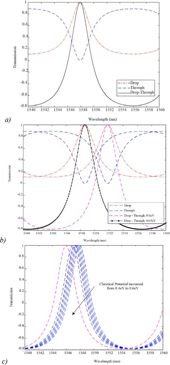
Fig. 5. (a) Normalized transmissions at through and drop ports, (b) the transmissions with two chemical potentials and (c) transmissions can be controlled by the change of chemical potential
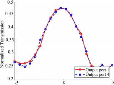
Next, we investigate the phase error of the 4×4 MMI based microring resonator. The phases at output ports 1 and 4 when input signal is at port 1 are shown in Fig. 7 b . The phase shift difference between port 1 and 4 is also presented in this simulation. The results show that the phase difference of 90 degree can be obtained over a length variation of 18 µm. This result provide a flexible design for the neuron element.
MMI length variation (/vm)
a)
400r
30(
y) loo
Cl- -100
-200
■ Output Ы
■Output b4
■e
b)
a)
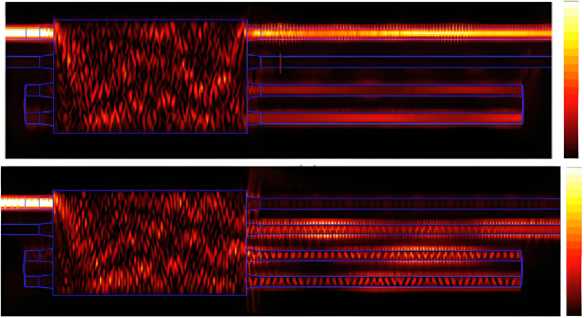
Fig. 6. (a) Signal propagation via the MMI based microring resonator with on resonance and (b) off-resonance
b)
-sour____
Length of 4x4 MMI (gm)
Fig. 7. (a) Fabrication tolerance analysis for variation of the 4×4 MMI length and (b) the phases at output ports 1 and 4 when input signal is at port 1
Some other performance parameters of the microring resonator are Finesse, Q-factor, resonance width, and bandwidth. These are all terms that are mainly related to the full width at half of the maximum (FWHM) of the transmission. The quality factor Q of the microring resonator of the structure in Fig. 1 can be derived as [21]:
Q =
к N g L R
X
Var1 -ar
Another important parameter for microring resonators is the finesse F, which is defined and calculated for the single and ad-drop microring resonators by:
F =
FSR
AX
FWHM
V ar
= к----
1 -ar
.
Where AX fwhm is the resonance fUll-width-at-half-maximum and FSR is the free spectral range. The Free Spectral Range (FSR) is the distance between two peaks on a wavelength scale. By differentiating the equation Ф = P L R , we get FSR = X 2/ n g L R , where the group index n g = n ff - X ( dn eff / d X ). The signal after the first neuron of the OONN in Figure 1 is modulated by a microring resonator modulator. For the first time, in this study, we use a 4×4 MMI resonator as shown in Fig. 8 a for the optical modulator. We use FDTD (Finite Difference Time Difference) method to simulate the proposed microring reso-
nator based on the multimode waveguide. In our FDTD simulations, we take in to account the wavelength dispersion of the silicon waveguide. A light pulse of 15 fs pulse width is launched from the input to investigate the transmission characteristics of the device. The grid sizes A x = A y = A z = 20 nm are chosen in our simulations for accurate simulations [22]. The FDTD simulations for the proposed microring resonator with chemical potentials of 0.45 eV and 0.42 eV are shown in Fig. 8 b and 8 c . The simulations show that the device operation has a good agreement with our prediction by analytical theory.
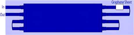
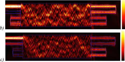
Fig. 8. (a) An MMI based resonator for optical modulator, (b) and (c) optical field propagation through the optical modulator based on an MMI resonator at different chemical potentials
The normalized transmissions of the propose microring resonator in Fig. 8 at microring radii of 5 ц m and 50 ц m are shown in Fig. 9. Here we assume that the chemical potential is ц c = 0.45 eV , the simulations show that the exact characteristics of a single microring resonator can be achieved. The very high FSR of the microring based on an MMI coupler can be obtained. This means that optical modulator with high bandwidth can be achieved. This is suitable for high speed and big data analytics using all-optical computing in the future. The FSRs can be calculated to be FSR = 100 nm for R =5 µ m and FSR = 10 nm for R =50 µ m , respectively.
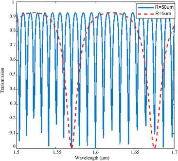
Fig. 9. Transmissions of the microring resonator with two microring radii of 5 ц m and 50 ц m
Fig. 10 illustrates the signal propagation through the whole structure at different chemical potentials for 0.6 eV and 0.65 eV . Input signals x 1 , x 2 , x 3 , x 4 are changed by controlling the potential chemicals at the MMI resonator for implantation of x 1 , x 2 , x 3 , x 4, respectively in Fig. 1.
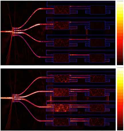
Fig. 10. Signal propagation via the whole device (a) chemical potential 0.6eV and (b) 0.65eV
In this work, we applied our proposed OONN to perform image recognition on the MNIST dataset. The optimized parameters to solve MNIST can be categorized in two groups [23], i.e., two 5 × 5 × 8 different kernels and two fully connected layers of dimensions 800 × 1 and 10 × 1 as presented in Fig. 11. We use the kernel filter 5 × 5 for simulations w11 w12 w13 w14
w21 w22 w23 w24
W = W 31
w34
w 41 w 42 w 43 w 44 w 45
w 51 w 52 w 53 w 54 w 55
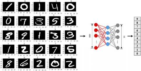
Fig. 11. OONN with two layers used for MNIST dataset recognition
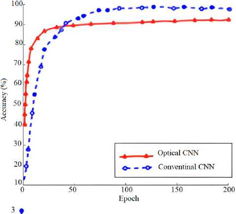
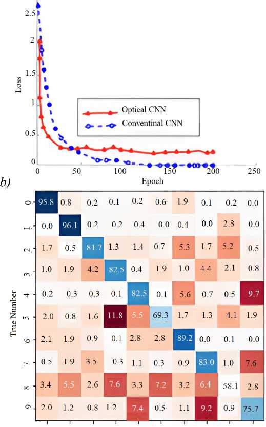
In this simulation, we use the OONN with two layers and the ReLU nonlinear activation function is used. The results of the MNIST task solved by our OONN is shown in Fig. 12a. Fig. 12a shows the simulated results of the overall accuracy of 92.4% after 10 interactions. We also compare the results with the conventional CNN consisting of two layers with an accuracy of 99.2 % after 50 interactions. Fig. 12b shows the loss. The simulation results show that the proposed structure can converge faster than the conventional CNN. Although the accuracy of the proposed OONN is lower than the standard CNN, the proposed structure is faster than 5 times and requires lower power consumption. This is suitable for higher connections with multiple layers in other complex applications. In addition, the standard CNN is a 32-bit floating point while the proposed structure uses only 6 bits of precision. The accuracy can be improved much more if we use the higher bit precision [24].
By cascading microring resonators based on 4×4 MMI to implement the neuron as shown in Fig. 1, for example with 100 microring resonators having the same radius of 5μm, the time propagating through the neuron is:
_ N(2 к R ) tp =—•
where c is the speed of light, R is the radius of the ring waveguide, N is the number of microring resonators. When N = 100 [9], the propagation time is t p = 11 ps and an throughput of 1/ t p = 100 ( GS / s ). The microring resonator covered with the graphene sheet can be modulated at speeds of 130 GS/s [25], meaning that the modulation frequency of the MRRs does not bottleneck the throughput of the neuron.
Next, we compare the performance of the proposed structure with DeepBench. DeepBench is a data set that contains how long various types of GPUs took to perform a convolution for a given set of convolutional parameters. The power usage of two of convolutional benchmarks for the GPUs from the DeepBench dataset are: AMD MI25 with 300W, Nvidia GTX 1080Ti with 250W [26, 27]. By using the proposed structure, the convonutional unit can produce a pixel of an image in 100 ps to perform a convolution with K filters using two pixels per circle. The speed of the convolution can be estimated by:
t runtime = 50 ps X K ( H - R + 1)( W - R + 1). (18)
Where R is the edge length of the kernel with zero padding, H and W are the height and width of the input image. The power consumption of the proposed convolution can be estimated at about 110W compared with mean GPUs power consumption of 295W. In addition, the speed of the proposed convolution is between 2.8 and 14× faster than mean GPU runtime.
Conclusion
In this paper, novel optical neural networks without the use of WDM and a new optical neuron that implements an optical vector-matrix multiplication (OVMM)
circuit employing multimode interference (MMI) structures are proposed. The microring resonator based on an MMI coupler is used for the optical modulator, add-drop weight banks for kernels and input signal encoding. The proposed structure has the benefits of not requiring WDM elements, having excellent manufacturing accuracy, being compact, and having low loss for higher layers CNN. We also showed how the OONN may be used to recognize handwriting in the MNIST dataset. The OONN is estimated to perform convolutions 2.8 to 14x times faster than a GPU while roughly using lower power consumption. Additionally, the suggested structure can handle both positive and negative numbers as well as more complicated jobs for upcoming applications that use the suggested OONN.
a)
0 1 2 3 4 5 6 7 8 9
Predicted number
c)
Fig. 12. (a) Accuracy, (b) loss and confusion matrix for MNIST recognition using standard CNN and the proposed OONN and (c) fusion matrix of the predicted numbers
Acknowledgement
This research is funded by Vietnam National Foundation for Science and Technology Development (NAFOSTED) under grant number 103.03-2018.354.
References On chip optical neural networks based on mmi microring resonators for image classification
- Xiang S, et al. A review: Photonics devices, architectures, and algorithms for optical neural computing. J Semicond 2021; 42(2): 023105. DOI: 10.1088/1674-4926/42/2/023105.
- Kazanskiy NL, Butt MA, Khonina SN, Optical computing: Status and perspectives. Nanomaterials 2022; 12(13): 2171. DOI: 10.3390/nano12132171.
- Sui X, Wu Q, Liu J, Chen Q, Gu G. A review of optical neural networks. IEEE Access 2020; 8: 70773-70783. DOI: 10.1109/ACCESS.2020.2987333.
- Yang L, Ji R, Zhang L, Ding J, Xu Q. On-chip CMOS-compatible optical signal processor. Opt Express 2012; 20(12): 13560-13565. DOI: 10.1364/OE.20.013560.
- Salmani M, Eshaghi A, Luan E, Saha S. Photonic computing to accelerate data processing in wireless communications. Opt Express 2021; 29(14): 22299-22314. DOI: 10.1364/OE.423747.
- Harris NC, et al. Linear programmable nanophotonic processors. Optica 2018; 5(12): 1623-1631. DOI: 10.1364/OPTICA.5.001623.
- Tait AN, et al. Feedback control for microring weight banks. Opt Express 2018; 26(20): 26422-26443. DOI: 10.1364/OE.26.026422.
- Le TT, Cahill LW, Elton D. The design of 2x2 SOI MMI couplers with arbitrary power coupling ratios. Electron Lett 2009; 45(22): 1118-1119.
- Ferreira de Lima T, et al. Design automation of photonic resonator weights. Nanophotonics 2022; 11(4-5): 49. DOI: 10.1515/nanoph-2022-0049.
- Zhang D, Tan Z. A review of optical neural networks. Appl Sci 2022; 12(11): 5338. DOI: 10.3390/app12115338.
- Tait AN, Nahmias MA, Shastri BJ, Prucnal PR. Broadcast and weight: An integrated network for scalable photonic spike processing. J Lightw Technol 2014; 32(21): 40294041. DOI: 10.1109/JLT.2014.2345652.
- Liu J, Khan ZU, Wang C, Zhang H, Sarjoghian S. Review of graphene modulators from the low to the high figure of merits. J Phys D: Appl Phys 2020; 53(23): 233002. DOI: 10.1088/1361-6463/ab7cf6.
- Xu X, et al. 11 TOPS photonic convolutional accelerator for optical neural networks. Nature 2021; 589(7840): 4451. DOI: 10.1038/s41586-020-03063-0.
- Zhang H, et al. An optical neural chip for implementing complex-valued neural network. Nat Commun 2021; 12(1): 457. DOI: 10.1038/s41467-020-20719-7.
- Bachmann M, Besse PA, Melchior H. General self-imaging properties in N x N multimode interference couplers including phase relations. Appl Opt 1994; 33(18): 3905-3911.
- Le TT. Multimode interference structures for photonic signal processing. LAP Lambert Academic Publishing; 2010.
- Bao Q. 2D Materials for photonic and optoelectronic applications. Woodhead Publishing; 2019.
- Xing P, Ooi KJA, Tan DTH, "Ultra-broadband and compact graphene-on-silicon integrated waveguide mode filters. Sci Rep 2018; 8(1): 9874. DOI: 10.1038/s41598-018-28076-8.
- Hanson GW. Dyadic Green's functions and guided surface waves for a surface conductivity model of graphene. J Appl Phys 2008; 103(6): 064302. DOI: 10.1063/1.2891452.
- Capmany J, Domenech D, Muoz P. Silicon graphene Bragg gratings. Opt Express 2014; 22(5): 5283-5290. DOI: 10.1364/OE.22.005283.
- Chremmos I, Schwelb O. Photonic microresonator research and applications. New York: Springer Science+Business Media LLC; 2010.
- Rumley S, et al. Optical interconnects for extreme scale computing systems. Parallel Comput 2017; 64: 65-80. DOI: 10.1016/j.parco.2017.02.001.
- Bangari V, et al. Digital electronics and analog photonics for convolutional neural networks (DEAP-CNNs). IEEE J Sel Top Quantum Electron 2020; 26(1): 5100209. DOI: 10.1109/JSTQE.2019.2945540.
- Zhang W, et al. Silicon microring synapses enable photonic deep learning beyond 9-bit precision. Optica 2022; 9(5): 579-584. DOI: 10.1364/OPTICA.446100.
- Wu L, Liu H, Li J, Wang S, Qu S, Dong L. A 130 GHz electro-optic ring modulator with double-layer grapheme. Crystals 2017; 7(3): 65. DOI: 10.3390/cryst7030065.
- AMD Radeon™ Instinct™ MI25 Accelerator. 2022. Source: https://www.amd.com/en/products/professional-graphics/instinct-mi25.
- NVidia. GeForce. Specifications. GeForce GTX 1080 Ti2022. Source: https://www.nvidia.com/en-gb/geforce/graphics-cards/geforce-gtx-1080-ti/specifications/.
