Optical and Electrophysical Properties of Thin Anisotropic Films Based on Carbyne Stabilized by Gold Particles

Author: Samyshkin V., Osipov A., Bukharov D., Lelekova A., Abramov A., Kuznetsov A., Kucherik A.
Journal: Компьютерная оптика @computer-optics
Section: XI International conference on information technology and nanotechnology
Article in issue: 6 т.49, 2025.
Free access
This study considers the optoelectrical properties of thin films composed of linear carbon stabilized by gold nanoparticles. We explore the unique anisotropic behaviors exhibited by these films and their dependence on the degree of structural ordering. The fabrication process includes the use of colloidal systems, with a focus on the laser-induced fragmentation of gold nanoparticles within a carbon matrix. Our findings reveal that applying a potential difference significantly alters the absorption characteristics of the films, particularly enhancing absorption at frequencies associated with short linear chains, while also inducing a transparency effect in the visible range. The introduction of electrons into the carbon matrix is identified as a key factor influencing these optical properties, drawing parallels to existing literature on resonance pumping phenomena. Additionally, the results indicate a considerable modification of the Schottky barrier at the semiconductor-metal interface due to structural orientation. This research provides insight into the potential applications of these materials in optoelectronic devices and highlights the importance of structural characteristics in tailoring their properties.
Optoelectrical properties, anisotropic properties, linear chains, semiconductor-metal interface
Short address: https://sciup.org/140313287
IDR: 140313287 | DOI: 10.18287/COJ1841
Text of the scientific article Optical and Electrophysical Properties of Thin Anisotropic Films Based on Carbyne Stabilized by Gold Particles
The fabrication of thin films exhibiting anisotropic optical or electrical properties is of significant interest for various practical applications [1]. This task is particularly crucial as substantial changes in the properties of the films are observed with decreasing thickness compared to the original bulk material [2]. The ability to combine materials with significantly different properties into a single film enhances anisotropic effects, typically achieved through layer-by-layer deposition with controlled layer thickness [3]. The creation of such thin films is a distinct and quite complex challenge, as the enhancement of their properties directly depends on maintaining the interfaces between materials [4]. For this reason, many researchers focus on producing one-dimensional structures, such as nanorods and wires, as their properties can be modified by varying aspect ratios [5]. However, elongated structures with lengths that vastly exceed their diameters do not represent true one-dimensional structures. Therefore, the utilization of linear carbon structures, which possess unique optical, electrical, and mechanical characteristics, appears promising [6].
This work presents results regarding the optoelectrical properties of thin films composed of linear carbon stabilized by gold nanoparticles. It is shown that the electrophysical properties of such films vary significantly with the degree of ordering of the deposited structures, and for ordered films, changes in optical absorption upon the application of an external electric field have been observed.
Furthermore, this research shows the potential of electroluminescence as a crucial mechanism for understanding the functional behavior of thin films. The observed electroluminescent properties not only offer insights into the fundamental processes governing light emission but also pave the way for innovative applications in optoelectronic devices. By exploiting these distinct characteristics, we can enhance the performance of light-emitting diodes (LEDs), solar cells, and sensors, thereby contributing to advancements in various fields such as telecommunications, energy generation, and environmental monitoring.
1. Method for fabricating thin films from linear carbon stabilized by gold nanoparticles
To form colloidal systems, we have employed the method described in [7]. The total volume of the colloidal system was 10 ml, consisting of 9 ml of an aqueous shungite solution [8] with a concen tration of 100 mg/ml and 1 ml of a colloidal gold solution with an average particle size of 5 nm and a concentration of 1 mg/ml. Fragmentation was carried out using laser radiation with a wavelength of 1.06 µm, pulse energy of 1 mJ, pulse duration of 100 ns, and a pulse repetition frequency of 20 kHz. The total time of laser exposure was 15 minutes.
Fig. 1 shows the TEM images of thin films which were formed by depositing small droplets of the colloid onto a substrate [9]; to ensure the orientation of the structures; the substrate was tilted after the droplet of the colloid had been fixed on its surface.
2. Comparison of optoelectrical properties of films with different degrees of disorder
We have previously described the results concerning conductivity changes in thin metal-carbon films under the influence of low-intensity pump radiation [10]. Our experiments demonstrate that in the case of resonance irradiation of terminal groups with gold particles, there is a significant increase in tunnel current when placing the probe over carbon structures [11], and changes in the bandgap width are also observed. Given that the bandgap width of linear chains is estimated in various studies to range from 1.6 to 4.1 eV depending on chain length and terminal groups [6, 12], a voltage range of [– 4, 4] V was selected for the study. Measurements were performed using a modified atomic force microscope, Integra-Aura, operating in scanning tunneling microscopy mode, with a measurement time of 1 second for each data point.
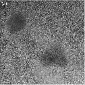
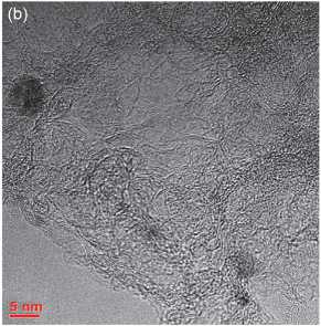
Fig. 1. TEM images of the deposited structures. (a) oriented bundles of chains, (b) random arrangements of linear chains
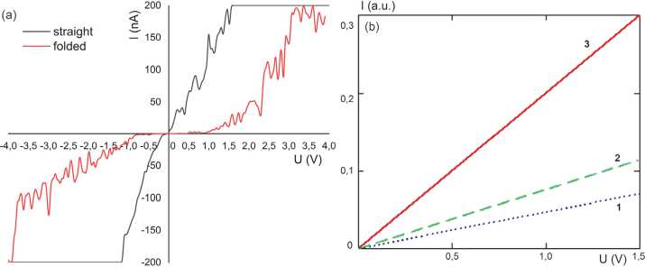
Fig. 2. I-V characteristics. (a) Experimentally measured rusults under irradiation as a function of nanoparticle concentration, (b) measurements for structures with varying fractal dimensions: 1 – D = 1, 2 – D = 1.6, 3 – D = 1.9
Fig. 2 a shows measurements of the tunnel current over the surface of the film irradiated by a continuous laser at a wavelength of 532 nm with a power output of 3 W, focused into a spot with a diameter of 2 mm near the probe. It is evident that the slope of the measured I-V characteristics differs significantly for the two presented films; nonetheless, there are also common features for both cases:
-
- both dependencies exhibit an asymmetrical shape, corresponding to the conditions for the formation of a Schottky barrier;
-
- periodic jumps in current indicate the presence of excess charges on the surface of the gold nanoparticles enclosed in the semiconductor matrix.
However, the slope of the I-V characteristic for the more ordered structures is significantly higher, and it exhibits a considerably lower number of oscillations, especially in the negative voltage region. To describe the measurement I-V characteristics features, a simple estimate of the resistance was made based on a fractal representation [13], approximating that the dominant contribution to the change in resistance results from the increase in the structure length, R~LD where L is the distance between contacts, D is the fractal dimension.
With significant twisting of the chains, the fractal dimension of the structure increases, approaching a value of 2. In the case of ordered arrangements, the fractal dimension varies slightly around a value of 1.
Fig. 2 b presents the I-V characteristics according to Ohm's law for chain segments in relative units for structures with different fractal dimensions: 1 corresponds to the linear structure, 2 to a sufficiently sparse bundle of chains, and 3 to a dense bundle of chains with a high filling degree.
Thus, the model dependencies qualitatively correlate with and do not contradict the measured values.
Since the optical and electrical properties of such films are interrelated, it is interesting to examine how the optical properties of oriented structures change when subjected to an external electric field. To facilitate this, gold contacts were evaporated onto the ends of the substrate, to which a potential difference of 1 V was applied, which, according to the measured I-V characteristics, should lead to significant changes in the measured optical characteristics.
The measurement was carried out using an integrating sphere, enabling the capture of changes in the absorption coefficient across the wavelength range (250-550 nm). This measurement range was chosen because the 250-400 nm spectral region is characteristic of short linear chains [14], while the plasmonic absorption of gold nanoparticles lies within the 510-550 nm region [15]. Notably, under the action of the electric field, the absorption in linear chains is enhanced, leading to a transparency effect in the visible range, so pronounced that the plasmon resonance of gold is not observed.
Such behavior can be associated with the active introduction of electrons into the carbon matrix, analogous to [9], where, under resonant pumping of the terminal groups, we were able to detect luminescence with an anti-Stokes shift. In this case, under the influence of the potential difference, electrons from the isolated gold particles within the semiconductor matrix gain enough energy to transition into the bundles of linear chains, which leads to an enhancement of absorption specifically at frequencies characteristic of short linear chains [16] without a frequency shift. This can also explain the observed transparency of the film in the 350-550 nm range.
Fig. 3 shows the difference between experimental results of the optical absorption of the film with oriented structures with or without field.
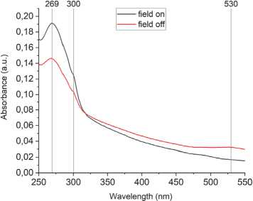
Fig. 3. Optical absorption of the film with oriented structures
3. Conclusion
This work presents the preliminary results of the study on the anisotropy of the optoelectrical properties of thin films composed of linear carbon fixed between gold nanoparticles. We have shown that the orientation of the structures significantly alters the Schottky barrier at the n-type semiconductor-metal interface, which can be attributed to the effective length of the fractal-type micro-contact. It is demonstrated that under the influence of a constant electric current, the absorption in the oriented thin film changes, with the absorption coefficient increasing for wavelengths typical of linear chains while decreasing in the visible wavelength range.
The observed effect enables the study of electroluminescence, providing valuable insights into the mechanisms underlying light emission in various materials. This phenomenon not only enhances our understanding of fundamental physical processes but also opens up new avenues for application in science and technology. By leveraging the tunable optoelectrical properties of the thin films, researchers can develop advanced optoelectronic devices, such as light-emitting diodes (LEDs), lasers, and displays. Additionally, these properties can be utilized in sensing technologies and energyefficient solutions, thus paving the way for innovative applications in diverse fields including telecommunications, medical devices, and renewable energy systems.
Further research in this area will focus on the effects of polarized optical radiation on the samples to demonstrate selective absorption by oriented bundles.
Acknowledgment
This work was supported by the framework of RSF grant 23-12-20004 and the state assignment in the field of scientific activity of the Ministry of Science and Higher Education of the Russian Federation (theme FZUN-2024-0019, state assignment of the VlSU).
