Platform independent implementation of high speed serial communication based on FPGA

Author: Raj Chanchal, Rajkumar Santosh Mohan
Journal: Журнал Сибирского федерального университета. Серия: Техника и технологии @technologies-sfu
Article in issue: 2 т.9, 2016.
Free access
In various embedded system applications, the high speed multi-serial communication is necessary. Various embedded systems require DSP (Digital Signal Processing) to process information & FPGA to control the peripheral devices. UART (Universal Asynchronous Receive Transmit) is designed in FPGA & connected to DSP so as to meet the real time capability of system along with compact, stable & reliable data transmission. In this paper we propose a software-implementation technique of an UART to get a platform independent UART-core for high speed serial communication in FPGA. Here the core is written in Verilog & implemented using XILINX ISE.
Fpga, verilog, uart
Short address: https://sciup.org/146115054
IDR: 146115054 | UDC: 621.391-026.51:004.4?2 | DOI: 10.17516/1999-494X-2016-9-2-189-196
Платформа независимой реализации высокоскоростной последовательной связи на основе FPGA
В различных приложениях необходимы встроенная система, высокая скорость мульти последовательной связи необходимо. Различные встроенные системы требуют DSP (цифровой обработки сигналов) для обработки информации FPGA для управления периферийными устройствами. UART (Universal Asynchronous Transmit) предназначен в FPGA и DSP и подключен таким образом, чтобы удовлетворить в реальном времени возможности системы наряду с компактной, устойчивой и надежной передачей данных. В этой статье мы предлагаем технику программного обеспечения Внедрение UART, чтобы получить платформу независимого UART-ядра для высокоскоростной последовательной связи в FPGA. Здесь ядро написано в Verilog и реализовано с использованием Xilinx ISE.
Text of the scientific article Platform independent implementation of high speed serial communication based on FPGA
Proposed architecture
-
A. Character Encoding
-
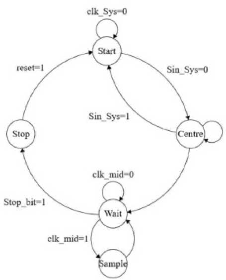
B. UART Receiver
The proposed receiver Finite State Machine has five states:
-
• Start state : the receiver Finite State Machine awaits the start bit, when the receiver is reset.
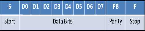
Fig. 1. Data Frame
-
• Centre state: receiver detect data after synchronizing the clock pulse. If baud rate synchronization fails then it returns to Start state.
-
• Wait state: it determines the length of bit frame for the state machine. After getting stop bit, next stop state comes.
-
• Sample state: when data bit has been sampled and tested, state machine would always transfer into Wait state and wait for the next data bit to come.
-
• Stop state: after getting new data, it changes the state to Start state.
-
C. UART Transmitter
The proposed transmitter Finite State Machine has five states:
-
• Rest state: before transmitting signal is initiated, the state machine remains in this state. After feeding data into input data bus of UART, Start state comes.
-
• Start state: in this state clock synchronization takes place after the transmitter transmits the start bit (logic 0 signal) & the state of the machine changes to P2S (Parallel to Serial Conversion state)
-
• P2S state: this state waits until data conversion from parallel to serial completes. After conversion, Shift state comes. Also, it is checked whether data frame has been completed or not. After completion of data frame state changes to Stop state.
-
• Shift state: The state machine immediately returns to P2S state after shifting the data to Tx.
-
• Stop state: in this state, stop bit (logic 1 signal) is transmitted, after completing the data frame, the machine returns to Rest state.
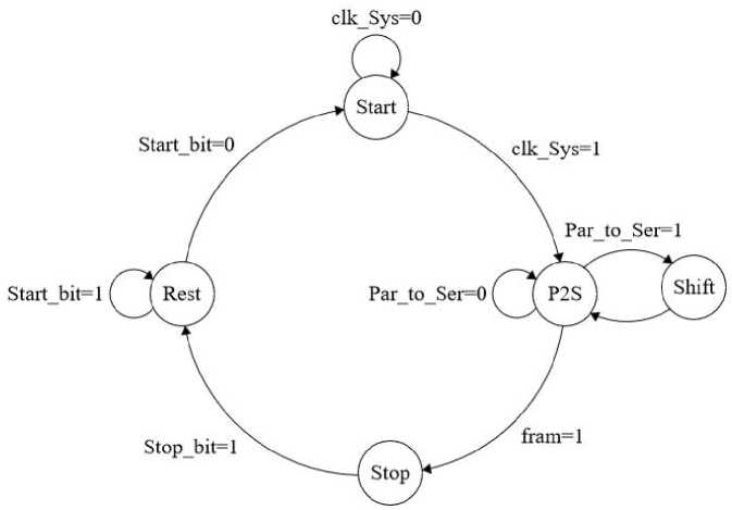
Table 1. Bit pattern of control register
|
C7 |
C6 |
C5 |
C4 |
C3 |
C2 |
C1 |
C0 |
Bit description: C7: – don’t care; C6: – no. of stop bits; C5, C4: – data bits; C3: – parity enable/disable bit; C2, C1, C0: – baud rate setting bits.
Table 2. Divisors for Baud rates
|
Clock = 50 MHz |
|||
|
Baud rate |
Divisor |
Baud rate |
Divisor |
|
57600 |
54 |
4800 |
651 |
|
19200 |
162 |
2400 |
1302 |
|
9600 |
325 |
1200 |
2604 |
-
D. Control Register
-
E. Baud rate generator
Baud rate generator is actually a clock divider circuit. It divides the system clock with suitable divisor to generate the desired baud rates. In this proposed model Baud rate error is minimized automatically. Table 2 represents the divisors used for the baud rate generated. The system clock is considered as 50 MHz.
The proposed uart module
The UART module has 4 internal blocks:
-
• Baud_Generator
-
• Operational_Unit.
-
• Interface_Unit.
-
• Tx_Rx_Unit.
-
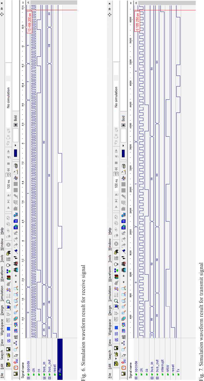
A. Simulation results
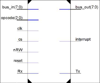
Fig. 4. UART top module
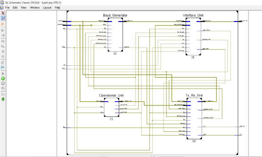
Fig. 5. Internal blocks of UART
The test ben c h wave forms for the receiver is shown in Fig. 6. Test bench generated signal ‘11001110’ (sequentially) is fed to the Rx line of the UART & simulation shows that the signal is appearing at ‘bus_out’ port.
The test bench wave forms for the transmitter is shown in Fig. 7. The test bench is feeding 8-bit data ‘00001010’ to ‘bus in’ port of UART in parallel. Simulation wave forms shows that the data is appearing at Tx line in accordance with bit frame.
Conclusion
References Platform independent implementation of high speed serial communication based on FPGA
- Zou Jie Yang,Jianning. Design and Realization of UART Controller Bas ed on FPGA
- Gallo R, Delvai M, Elmenreich W, Steininger A, Revision and verification of an enhanced UART, 2004, Proceedings, 2004 IEEE International Workshop on Factory Communication Systems, pp. 315-318, 22-24, Sept. 2004
- Zhang xue, Xu xiaosu, Zhang guolong. Design of High Speed Serial Communication Based on DSP and FPGA. Ship Electronic Engineering, 2009, 29(5), 66-68
- Xilinx Inc., Command Line Tools User’s Guide, URL: www.xilinx.com, accessed at: February 2014
- James O. Hamblen, Tyson S. Hall, Michael D. Furman. Rapid prototyping of digital systems, 2nd ed., springer Publication, 2001
