Power Optimization of Configurable Logic Block in FPGA via Controlling Logic State of Virtual Ground Voltage

Author: Shoaib Shokuhi, Ali Hosseini
Journal: International Journal of Image, Graphics and Signal Processing(IJIGSP) @ijigsp
Article in issue: 2 vol.8, 2016.
Free access
In this article, power optimization is investigated in Configurable Logic Block (CLB) of Field Programmable Gate Array (FPGA) for 65nm technology via controlling Virtual Ground Voltage (Vssv) state that follows Power-Gated standard. Initially different Configurable Logic Block are designed through the logic gates and then expanded via adding Look Up Table circuit (LUT) in inputs; afterwards, the samples of Configurable Logic blocks are investigated in two logic states of Virtual Ground Voltage =0 and Virtual Ground Voltage =1 regarding the power dissipation; whereas 100µs is time reference for simulation of time controller of Virtual Ground Voltage function. First Configurable Logic Block are kept at logic state of Virtual Ground Voltage =1(power gated) for 10µs out of 100µs and remaining time at logic state of Virtual Ground Voltage =0 (power not gated); then the simulation test is repeated up to 50µs in 5 steps for each Configurable Logic Block sample. Finally the result shows that reduction being at logic state of Virtual Ground Voltage =0 in a constant time period has linear effect on decreasing average power. With the Configurable Logic Block in operation for 50% of the total time in Virtual Ground Voltage =1 logic state, the average power reduces up to 49% in the best case scenario. Meanwhile the Configurable Logic Block can still preserve its logic state.
Power optimization, logic gates, Field Programmable Gate Array, simulation, power gated, look up Table, Configurable Logic Block, Virtual Ground voltage
Short address: https://sciup.org/15013951
IDR: 15013951
Text of the scientific article Power Optimization of Configurable Logic Block in FPGA via Controlling Logic State of Virtual Ground Voltage
Published Online February 2016 in MECS
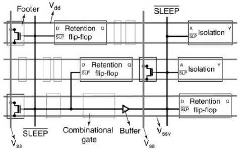
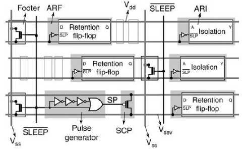
Increased usage of FPGA in portable devices and becoming smaller in size with every generation process, causes increase in power consumption [1] thus, structure should be modified through presenting new methods and modification of internal block for reducing power. In a digital complementary metal–oxide–semiconductor (CMOS) circuit, dynamic power dominates the total- power dissipation. Reducing the supply voltage Vdd is the most effective approach to reduce dynamic power dissipation. Lowering Vdd is also important in deep submicron (DSM) technologies to avoid reliability problems [2]. However, reducing the supply voltage alone causes serious degradation in the circuit’s performance. One way to maintain performance is to scale down both Vdd and the threshold voltage Vth. However, reducing Vth increases the subthreshold leakage current exponentially [3]. Integrated low-power architecture is proposed and implemented for FPGA, which fully utilizes the fine-grain assignment of VDD/VTH in time and space that way, 4 Configurable Logic Blocks (CLB) are grouped into one block where is shared [4]. In [5] average switching activity of the input and output state variables is reduced by minimizing the number of bit changes during state transitions. In [6] a variable threshold voltage as keeper circuit techniques proposed for simultaneous power reduction. Power gating [7]–[8] is the most popular circuit technique to suppress subthreshold leakage. It consists of gating, or cutting off, a circuit from its power supply rails during standby mode. When footer, located between a logic block and Vss, is turned off, the voltage at virtual ground (Vssv), where footer has its drain, rises slowly until it reaches a steadystate potential, which is usually close toVdd. Similarly, if a header is used and if it is turned off, the voltage at virtual Vdd (Vddv), slowly goes down to a steady-state potential, which is close to Vss. Due to collapse of either Vssv or Vddv during standby, the circuit states that are represented by sequential elements and primary outputs have to be captured in advance and preserved. Data retention elements (flip-flops and isolation circuits) are used to preserve circuit states during standby mode, if the states are needed again after wake-up. These elements must be controlled by an external power management unit, causing a network of control signals implemented with extra wires and buffers. A power-gated circuit with autonomous data retention (APG) is proposed in [9] to remove the overhead involved in control signals. Retention elements in APG derive their control by detecting rising potential of virtual ground rails when power gating starts, i.e., they control themselves without explicit control signals. APG and standard PG are shown in figure 1. In both circuits, combinational gates are placed between Vdd and Vssv. Vssv gets controlled through footer, that way it is powered on, in an active state and powered off in a standby state. In APG [9], storing Flip flop and isolation circuits are replaced with Autonomous Retention Flip Flop (ARF) and Autonomous Retention Isolation (ARI). ARF and ARI are used for storing data while footer is off. For this purpose one slave latch, which is in charge of ongoing data, is connected directly to Vss and Vdd to capture Flip flop data [9]-[10]. In [11] area-efficient circuits for programmable fine-grained power-gating of individual unused interconnect switches is presented. Fine-grain power gating is more effective than coarse-grain power gating to reduce the active leakage power of unused logic and interconnection resources [12]. In [13] a modification to the fabric of an FPGA is presented that enables dynamically-controlled power gating, in which logic clusters can be selectively powered-down at run-time. Detecting the data arrival in advance prevents the delay increase for waking-up and the power consumption of unnecessary power switching [14]. In [15] architecture is presented that enables selectively powering down SBs along with the logic blocks during their idle periods. In [16] a tool is presented that capable of modeling the power usage of many different field programmable gate array (FPGA) architectures. In [17] a novel directional coarse grained power gating architecture for switch boxes is presented. In [18] an FPGA architecture is presented that enables dynamically controlled power gating, in which FPGA resources can be selectively powered down at run-time. In [19] area, delay, and energy for two intra-CLB topologies are compared. Figure 2 shows how logic blocks get controlled through Vssv state via footer switch. In this paper by controlling time period of Vssv logic state through Footer switch, power dissipation in CLB block is investigated. First in section 2, power consumption for 5 sample circuits of CLB block is investigated. In section 3, we apply our method for reduction of power dissipation and test it through the sample CLB blocks; finally in section 4 we show result of power recovery in the sample CLB blocks. In this paper when we mention Vssv=1 or 0, we describe Vssv logic state, not its voltage.
(a)
(b)
Fig.1. a. Standard PG [9] and b. APG [9]
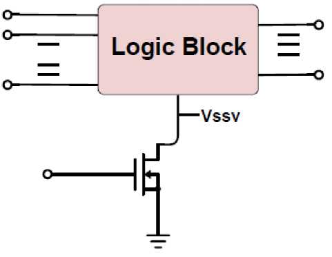
Fig.2. Footer switch in logic block
-
II. Method of Power Consumption Simulation on 5 Samples of CLB Blocks
-
A. Clb Design through Transistor Model of Logic Gates
Basic logic gates (NOT, AND, OR,...) are simulated through NMOS and PMOS model in 65nm technology for design of CLB block in FPGA. Structure of CMOS model for Inverter, 2-input NAND, 2-input NOR and SR Flip flop, is used in this research, shown in figure 3.
Utilizing these CMOS transistor models, we are able to design the main blocks in FPGA, since architecture of CLB block is made through Logic gates. Initially in the simulation process, Flip flop is designed through combination of transistor model of (OR), (AND) and (NOT) gates. Then through synthesis of two (AND), one (NOT) and one (OR), (MUX-2 input) is acquired (depending on amount of inputs in MUX). Afterward via utilizing the logic gates, (LUT) is modeled and in result by using MUX, LUT and F.F, CLB block, which is most important block in FPGA, is obtained. Following which, power dissipation of each logic gate, which contributes in CLB block design, is investigated.
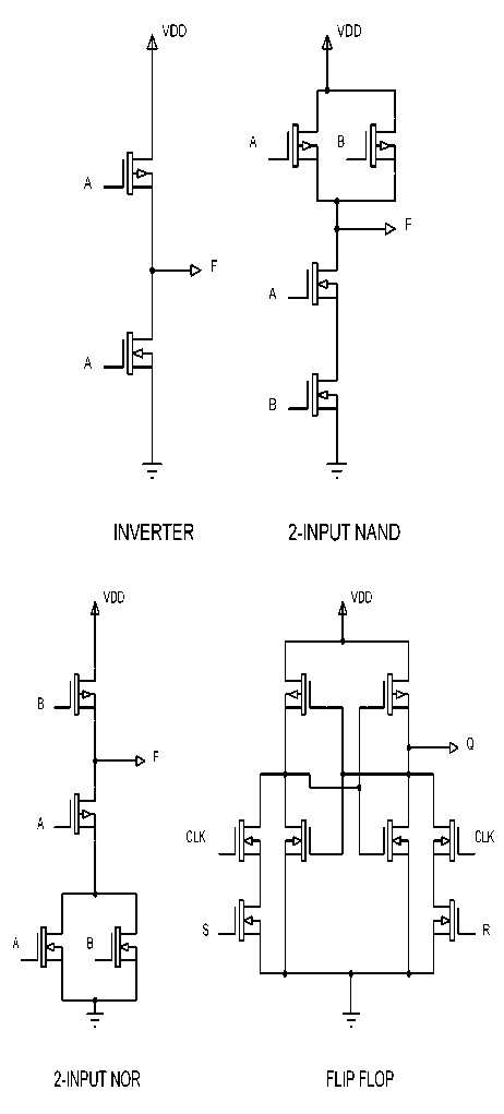
Fig.3. CMOS transistor model used in logic gates and flip-flop for design of the CLB block
-
B. Power Equations
Allowable power consumption is main concern while expanding integration in circuits as well as processing speed. Depending on the design, different formulas can be considered for power dissipation. When it is required to assign voltage and current in power supply, peak power factor is more useful, when battery consumption and cooling system is the main concern, then Pav factor becomes a preferable parameter that is shown in (1) [20].
w = 1 XJtP(td = -SUp XJtIsup(tdt (1)
In formula (1) , P(t) is transition power, I sup is the amount of current that is drawn from V sup in period of E(o. ‘ ] .
Table 1. Power dissipation for logic gates, Flip flop, Mux and CLB
|
Gate |
Power Dissipation |
|
NOT |
18µw |
|
NAND |
60µw |
|
XOR |
1/2mw |
|
FLIP FLOP |
600µw |
|
MUX |
600µw |
|
LUT |
600µw |
|
CLB TEST |
70mw |
After acquiring power dissipation, in proportion with given input and transistor CMOS model for each gate, final results are concluded in table 1. Table 1 shows average power ( P av ) of logic gates, Flip flop, Mux, LUT, CLB.
-
C. Implementation of Sample Circuits on CLB Block
In figure 4, internal schematic of CLB block, which designed through logic gates and flip flop, is shown that includes LUT at input, MUX in middle and Flip flop at output. The main CLB block is utilized as the first sample circuit under test. In this paper 5 sample circuits are presented on basis of the CLB block shown in figure4; in each one, 2 logic gates are added to LUT section of last sample circuit in order to investigate and compare power dissipation on these sample circuits.
Table 2. Added logic gates to LUT of the sample CLB circuits
|
The 5 samples of CLB blocks |
||||||
|
I |
II |
III |
IV |
V |
||
|
i e 3 H p p |
G1 |
XOR |
XOR |
XOR |
XOR |
XOR |
|
F1 |
OR |
OR |
OR |
OR |
OR |
|
|
G2 |
NAND |
NAND |
NAND |
NAND |
NAND |
|
|
F2 |
AND |
AND |
AND |
AND |
AND |
|
|
G3 |
AND |
AND |
AND |
AND |
||
|
F3 |
XOR |
XOR |
XOR |
XOR |
||
|
G4 |
AND |
AND |
AND |
AND |
||
|
F4 |
OR |
OR |
OR |
|||
|
G5 |
NAND |
NAND |
||||
|
F5 |
OR |
OR |
||||
|
G6 |
XOR |
|||||
|
F6 |
NAND |
|||||
According to internal architecture of designed CLB block in figure (4), logic gates are added to initial LUT section as presented in table 2. Accordingly in each sample circuit, one LUT block includes 2 logic circuits are added to last sample circuit so that from 4 input gates in first sample circuit, it is expanded to 12 input gates in 5th circuit. In figure (4) respectively XOR-OR-NAND-AND are used in LUT section .
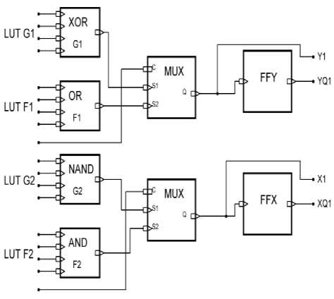
Fig.4. Design of CLB block through the logic gates (I sample CLB)
-
D. Dissipation Power in First Sample Circuits
Main CLB block architecture is utilized as the first sample circuit under test. In this test, dissipation power is investigated through simulation in two logic state of V ssv =0 and V ssv =1 . Results in Table 3 shows that dissipation power is reduced in Vssv =1 state.
-
E. Dissipation Power in 5th Sample Circuits
In 5th sample circuit, else LUT is added to 4th sample circuit includes (G6(XOR)-F6(NAND)) and totally compared to main CLB circuit, 4 LUT include ((G3(AND), F3(XOR), G4(AND), F4(OR), G5(NAND), F5(OR), G6(XOR), F6(NAND)) is added to inputs that shown in figure 5. The power dissipation of 5th sample circuit, in two logic states of V ssv =0 and V ssv =1, is shown in table 3(V). According to obtained result, despite expanding CLB block through added LUT, dissipation power reduced dramatically via keeping V ssv at state of logic 1.
Table 3. Dissipation power of sample circuits of CLB at logic state of V ssv =1 ( P Gated ) and V ssv =0 ( P not Gated )
|
Logic State |
I |
II |
III |
IV |
V |
|
Vssv =0 ( PGated ) |
75mw |
125mw |
165mw |
205mw |
250mw |
|
V ssv =1 ( PnotGated ) |
350uw |
525uw |
700uw |
870uw |
1.8mw |
-
F. Dissipation Power Results in Sample Circuits
In table3, power dissipation for 5 sample circuits in two logic states of Vssv=1 and Vssv=0 is compared and shows despite expanding LUTs in CLB, at state of Vssv=1 (Power gated) power is reduced.
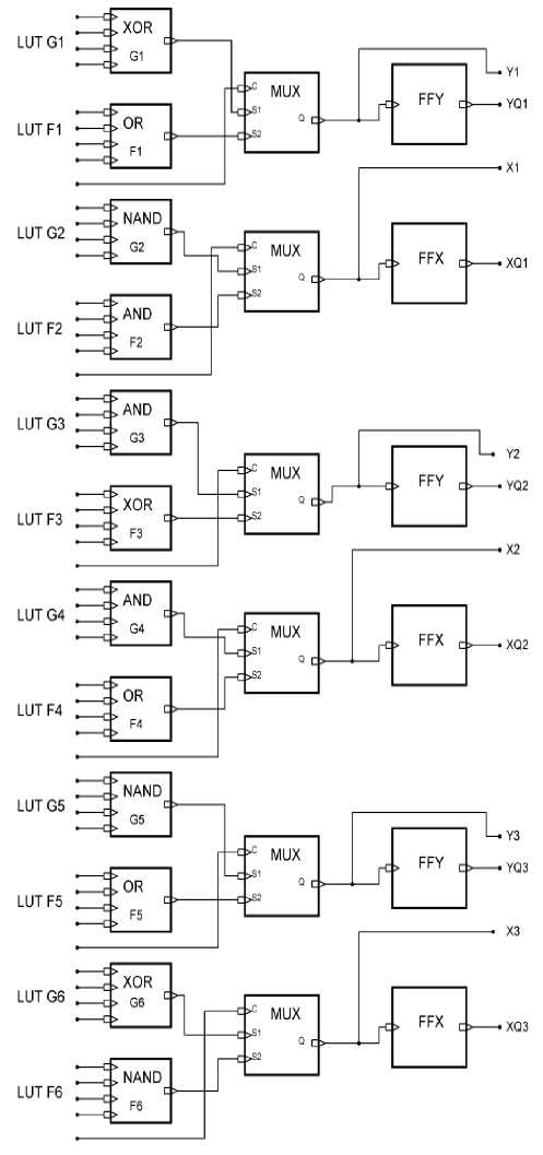
Fig.5. V (5th) sample circuit of CLB block
-
III. Our Proposed Method for Power Recovery
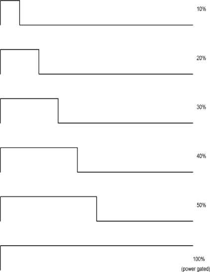
According to obtained results, we analyze effect of PGated (power consumption in power-Gated state)and Pnot Gated (power consumption in full function state) in the CLB blocks by time controller of Vssv logic state and evaluate it through power recovery factor in different CLB blocks. First 100µs is considered as a time reference for state of V ssv in 5 samples of CLB blocks then according to time intervals out of 100µs power get evaluated in power gated state( V ssv =1 ). Below formula is used for calculation of power dissipation in CLB samples. In equation 2, T is Time reference and is equal to
T=100µs and ( per ) is the period for which Vssv=1 . Time period for the logic states of Vssv=1 and Vssv=0 is shown in figure 6.
|
PeLvP f P Gated I ^ x P Gated I +( I |
per - T |
^ x P notGated ) |
|
T |
(percentage of being at state of Vssv=1)
0%
(power not gated)
—I----------1----------1----------1----------1----------1----------1-----------1----------1-----------1----------г
0 10 20 30 40 50 60 70 80 SO 100
Time (us)
Fig.6. Time period for the logic states of Vssv=1 and Vssv=0 in the method
Table 4. Power dissipation for different percentages of being at state of P gated (V ssv =1 ) out of 100µs and P not gated (0% out of 100 µs at state of V ssv =1 ) in the CLB sample circuits.
|
No. |
10% Mw |
20% (Mw) |
30% (Mw) |
40% (Mw) |
50% (Mw) |
P gated 100% (µW ) |
P notgated 0% (Mw) |
|
I |
67 |
60 |
52 |
45 |
37 |
350 |
75 |
|
II |
112 |
100 |
87 |
75 |
62 |
525 |
125 |
|
III |
148 |
132 |
115 |
99 |
82 |
700 |
165 |
|
IV |
184 |
164 |
143 |
123 |
102 |
870 |
205 |
|
V |
225 |
200 |
175 |
150 |
125 |
1800 |
250 |
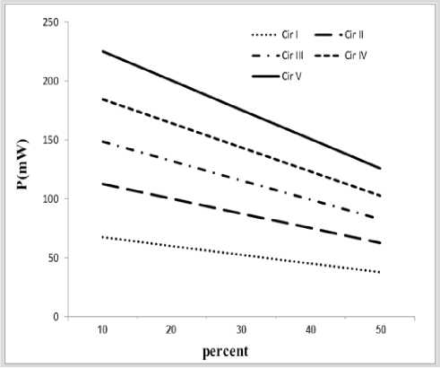
Fig.7. Reducing power according to percentage of period of time that Vssv=1 out of 100µs in 5 sample circuits of CLB
Power Recovery is a factor that indicates power reduction in sample circuits of CLB block. Result in table 5 shows being in logic state of Vssv=1 , raises Recovery power factor. Moreover row I to V shows power recovery between 10% to 50% in (per) (period of time that Vssv=1 out of 100µs ). ( Avg ) shows average power recovery in 5 sample circuits. Linear relation of Average power reduction versus per ((percent of time out of 100µs that Vssv=1 ) is presented in Figure 8. It indicates that despite number of LUT used in CLB block, lowering activity of V ssv (being at logic state of Vssv =1 for longer) results in, higher power recovery.
-
IV. Result
In table 4 power dissipation is considered in column 2 up to 6 in ( per ) interval for 10µs up to 50µs out of 100µs in 5 steps for sample circuits of CLB. Column 7 and 8 respectively show power dissipation in power gated state and power not gated state.
According to figure 7, as much as ( per) period (period of time that V ssv =1 ) gets longer, power dissipation get less, thus The power reduction is in linear proportion with ( per ); in addition, slope of lines become more along with expanding the sample circuits of CLB.
Power Recovery = ( --- — )x 100 (3)
P notGated
For obtaining maximum power saving, it requires to keep V ssv =1 for 50% of total duty cycle that cause 49% saving in energy but in contrast extra delay will be imposed that limits our method to just low speed application. By using less percentage of duty cycle being at state of V ssv =1 , energy optimization get reduced but it rises time efficiency and in result it will lead to fast performance, though the method can be adjusted according to the design and application. By using Power
Recovery factor, it is possible to measure energy saving through controlling duty cycle time of Vssv in operation that can be applied to previous works that requires more power saving and less speed.
Table 5. Power Recovery in the sample circuits of CLB according to percentage of time out of 100µs in logic state of Vssv=1
|
Sample CLB Circuit No. |
Power recovery (mw) according to time percentage of being at Vssv=1 state |
||||
|
10% (mw) |
20% (mw) |
30% (mw) |
40% (mw) |
50% (mw) |
|
|
I |
9.953 |
19.906 |
29.86 |
39.813 |
49.766 |
|
II |
9.958 |
19.916 |
29.874 |
39.832 |
49.79 |
|
III |
9.957 |
19.915 |
29.872 |
39.830 |
49.787 |
|
IV |
9.957 |
19.915 |
29.872 |
39.830 |
49.787 |
|
V |
9.928 |
19.856 |
29.784 |
39.712 |
49.64 |
|
Avg |
9.950 |
19.901 |
29.852 |
39.803 |
49.754 |
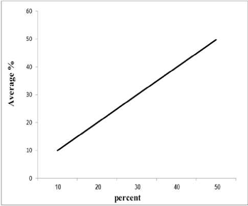
Fig.8. Average power reduction against percentage of being at logic state of Vssv =1 out of 100µs
-
V. Related Work and Discussion
Approximately 16 percent of the FPGA power is consumed by the CLBs alone [21]. As technology nodes scale down, the leakage power is going to increase in these logic blocks. Also, its effects on the total power should not be ignored for FPGA cores that can be embedded within an ASIC architecture [21]. The components of the CLB are latches (in place of SRAM cells), Muxes, and flip-flop. The methods considered in previous works are multi-threshold CMOS, clock gating, and variable gate length transistors [21]. Previous work on creating a low energy FPGA, explored many architectures and circuit techniques. [22] The lookup table size was chosen because previous studies revealed that it is a good choice for speed and density. A variable gate length method was introduced to reduce the power consumption of the CLB. Variable gate length transistors allow for the reduction of leakage in circuits that do not require high performance. The clock gating of the D flipflop isn’t required to be fast if the flip flop is not switched very frequently. Therefore, the clock gating circuitry can slowly compare the input and output of the flipflop and have a value ready when the flipflop is clocked. This method reduced the power consumption for the sequential mode by reducing the leakage in those gates. The comparison of the three CLB power reduction methods can be seen in Figure 9. The delay of the logic block increases when the clock gating technique is integrated. The addition of the variable gate length transistors only increases the delay slightly but results in a large reduction in power consumption [21]. In this paper power optimization of CLB by utilizing time controlling of virtual ground (Vssv) is investigated and in result, it showed that by CLB in operation for 50% of the total time in Vssv =1 logic state, the average power reduces up to 49%, but depends on application of design, whether, it will allow designer to keep the CLB off for the special period of time. By merging this method with previous works, there will be more potential for reducing power dissipation that can be accomplished in future works.
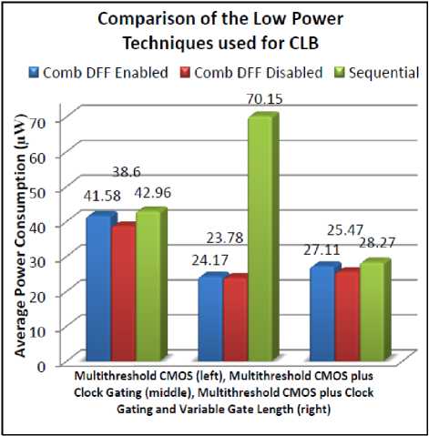
Fig.9. Power of optimized CLB in previous works (f=200MHZ) [21]
-
VI. Conclusion
In this research initially power consumption of logic gates that contribute in CLB block design is obtained, then through investigating internal block of CLB in FPGA at 2 logic states of Vssv=1 and Vssv=0, reducing power is considered. In result, it is observed that, via adding logic gates in LUT section of CLB, power dissipation through controlling Vssv state is changed dramatically, such that when Vssv=0, power is raised and in case of Vssv=1, circuit goes to power gated state and power dissipation get reduced. Results also show that there exist linear equation among average power reduction and activity of Vssv in sense of time interval. In this research initially 100µs is considered as a time reference for controlling Vssv logic state such that, the sample circuits of CLB are tested between 10µs to 50µs out of 100µs at logic state of Vssv=1 and remained time of 100µs at logic state of Vssv=0. Result shows that, staying on power gated state for 10% up to 50% of total time, can reduce power dissipation, respectively 9% to 49%. By presenting time controller of Vssv logic state, power is optimized while having a criterion of power dissipation measurement for power gated state (Vssv=1). In addition when Vssv=1 and circuit is in Power gated state, logic state can be preserved and this preserving logic state, leads to reducing power dissipation.
Acknowledgment
The authors wish to thank Dr. Hadi Jahanirad for his technical support.
References Power Optimization of Configurable Logic Block in FPGA via Controlling Logic State of Virtual Ground Voltage
- J. Friedrich, B. McCredie, N. James, B. Huott, B. Curran, E. Fluhr, E.Chan, G. Mittal, D. Plass, Y. Chan, S. Chu, H. Le, L. Clark, J. Ripley, S. Taylor, J. Dilullo, and M. Lanzerotti, "Design of the Power6 microprocessor,"in Proc. IEEE Int. Solid-State Circuits Conf., Feb. 2007,pp. 96–97.
- H. Iwai, "CMOS Technology—Year 2010 and Beyond," IEEE J. Solid-State Circuits, vol. 34, pp. 357–366, Mar. 1999.
- Anis, M.H.; Allam, M.W.; Elmasry, M.I., "Energy-efficient noise-tolerant dynamic styles for scaled-down CMOS and MTCMOS technologies," in Very Large Scale Integration (VLSI) Systems, IEEE Transactions on , vol.10, no.2, pp.71-78, April 2002
- Tran, C.Q.; Kawaguchi, H.; Sakurai, T., "95% Leakage-Reduced FPGA using Zigzag Power-gating, Dual-VTH/VDD and Micro-VDD-Hopping," in Asian Solid-State Circuits Conference, 2005 , vol., no., pp.149-152, Nov. 2005
- L.Benini and G.D.Mecheli. "State assignment for low power dissipation" IEEE J Solid- state circuits, vol 30, no.2, pp.258-268, mar. 1995.
- Kursun, V.; Friedman, E.G., "Domino logic with variable threshold voltage keeper," in Very Large Scale Integration (VLSI) Systems, IEEE Transactions on , vol.11, no.6, pp.1080-1093, Dec. 2003
- S. Mutoh, T. Douseki, Y. Matsuya, T. Aoki, S. Shigematsu, and J. Yamada, "A 1-V power supply high-speed digital circuit technology with multithreshold-voltage CMOS," IEEE J. Solid-State Circuits, vol. 30,no. 8, pp. 847–854, Aug. 1995.
- S. G. Narendra and A. Chandrakasan, Eds., Leakage in Nanometer CMOS Technologies. New York: Springer, 2005.
- J.Semon and Y.Shin "Design and optimization of Power-Gated circuits with autonomous data retention," IEEE TRANSACTION ON [VLSI]SYSTEMS ,VOL 19,no.2, pp.227-235,feb 2011 .
- H. Mair, A.Wang, G. Gammie, D. Scott, P. Royannez, S. Gururajarao, M. Chau, R. Lagerquist, L. Ho, M. Basude, N. Culp, A. Sadate, D. Wilson, F. Dahan, J. Song, B. Carlson, and U. Ko, "A 65-nm mobile multimedia applications processor with an adaptive power management scheme to compensate for variations," in Proc. Symp. VLSICircuits, Jun. 2007, pp. 224–225.
- Yan Lin; Fei Li; Lei He, "Routing track duplication with fine-grained power-gating for FPGA interconnect power reduction," in Design Automation Conference, 2005. Proceedings of the ASP-DAC 2005. Asia and South Pacific , vol.1, no., pp.645-650 Vol. 1, 18-21 Jan. 2005
- Rahman, Arifur; Das, S.; Tuan, T.; Trimberger, S., "Determination of Power Gating Granularity for FPGA Fabric," in Custom Integrated Circuits Conference, 2006. CICC '06.IEEE , vol., no., pp.9-12, 10-13 Sept. 2006
- Bsoul, A.A.M.; Wilton, S.J.E., "An FPGA architecture supporting dynamically controlled power gating," in Field-Programmable Technology (FPT), 2010 International Conference on , vol., no., pp.1-8, 8-10 Dec. 2010
- Ishihara, S.; Hariyama, M.; Kameyama, M., "A Low-Power FPGA Based on Autonomous Fine-Grain Power Gating," in Very Large Scale Integration (VLSI) Systems, IEEE Transactions on , vol.19, no.8, pp.1394-1406, Aug. 2011
- Bsoul, A.A.M.; Wilton, S.J.E., "An FPGA with power-gated switch blocks," in Field-Programmable Technology (FPT), 2012 International Conference on , vol., no., pp.87-94, 10-12 Dec. 2012
- Goeders, J.B.; Wilton, S.J.E., "VersaPower: Power estimation for diverse FPGA architectures," in Field-Programmable Technology (FPT), 2012 International Conference on , vol., no., pp.229-234, 10-12 Dec. 2012.
- Chin HauHoo; Yajun Ha; Kumar, A., "A directional coarse-grained power gated FPGA switch box and power gating aware routing algorithm," in Field Programmable Logic and Applications (FPL), 2013 23rd International Conference on , vol., no., pp.1-4, 2-4 Sept. 2013
- Bsoul, A.A.M.; Wilton, S.J.E.; Tsoi, K.H.; Luk, W., "An FPGA Architecture and CAD Flow Supporting Dynamically Controlled Power Gating," in Very Large Scale Integration (VLSI) Systems, IEEE Transactions on , vol.PP, no.99, pp.1-1, feb. 2015
- Ayorinde, Oluseyi; He Qi; Yu Huang; Calhoun, Benton H., "Using island-style bi-directional intra-CLB routing in low-power FPGAs," in Field Programmable Logic and Applications (FPL), 2015 25th International Conference on , vol., no., pp.1-7, 2-4 Sept. 2015
- RABAEY, J; CHANDRAKASAN, A.; NIKOLIC, B. Digital Integrated Circuits: a design perspective. 2nd Edition. Prentice Hall, 2003. ISBN: 0-13-090996-3.
- Bhavya Daya; Low-Power Configurable Logic Block (CLB) Design for FPGAs, http://web.mit.edu/ 2009
- George, V., et al., "The Design of a Low Energy FPGA," ISLPED 1999.
