Prediction of Intermittent Failure by Presage Debacle Model in Network on Chip

Author: Sangeeta Singh, J. V. R. Ravindra, B. Rajendra Naik
Journal: International Journal of Computer Network and Information Security @ijcnis
Article in issue: 4 vol.14, 2022.
Free access
With the emergence of deep sub-micron technology, the reliability issues in on-chip interconnect has enormously increased. This includes single event upsets, like soft errors, and hard faults which are rapidly becoming important factors to be considered. Aggressive technology scaling renders these architectures vulnerable to system performance, intermittent failure, capacitive crosstalk, and power dissipation problem. To improve the performance of the area and power consumption along with bandwidth, throughput and latency, a Buffer Potency Power Gating Technique is carried out to predict the Intermittent Failure by Presage Debacle Model in Network on Chip. In the Presage Debacle Model, the links present in the application-specific topology are provided with real application traffic to assist in prediction of the intermittent failure. By predicting the failure, the output of the model provides the power dissipated over the connection of the application link. Then the crosstalk noise in the topology is reduced by the Adaption of Simulated Annealing (SA) based Particle Swarm Optimization (PSO) congruence algorithm. The optimization congruence algorithm assigns each task in the application software to each node in the topology to determine the network's optimal output. It continuously changes the task park position in the topology system and reduces the crosstalk of the NoC. Consecutively, the area and power consumption are minimized by Buffer Potency Power Gating Technique. Buffer efficiency is increased and the power-gating is a practical way to mitigate NoC power control schemes properly and effectively without any loss in performance. Thus the prediction of intermittent failure is obtained by utilizing NoC to improve the performance of area and power consumption.
Network on Chip (NoC), Intermittent Failure, Crosstalk Noise, Power gating
Short address: https://sciup.org/15018477
IDR: 15018477 | DOI: 10.5815/ijcnis.2022.04.06
Text of the scientific article Prediction of Intermittent Failure by Presage Debacle Model in Network on Chip
Over the past few years, with technology advancements, the number of processors, DSPs, memory elements, and Intellectual Property (IP) cores on the Chip System (SoC) has risen. This exponential growth in the number of elements upon a single chip has increased complexity in processing and connectivity. As a result, today's SoCs require an energyefficient and high-performance on-chip communication medium [1]. Networks-On-Chip (NoC) has emerged as a feasible approach for modeling energy-efficient and high-performance connectivity architectures particularly for MultiProcessor SoC (MPSoC) [2]. The architecture of the topology in NoC affects the overall efficiency, power consumption and area of the chip.
Data transmission between various cores is achieved across an on-chip network formed using routers and links in the NoC paradigm. A network interface (NI) node connects the core to the router, and each router is linked by point-to-point connections. The data can be routed through the connections with the help of the routers. The network interfaces receive/transmit data coming from or going to the network's root [3].When a large number of system components are used in conjunction, there can be a lot of communication and data sharing between the components. Thus if there exists high degree of connectivity among the components, as is the case with the majority of modern implementations, leads to the problem of congestion because of the network traffic density. As a result, the NoC architecture and the paths between nodes must be carefully designed to ensure that performance constraints are satisfied [4]. The selection of topology as a network design process is influenced by a number of factors, namely bandwidth, productivity, energy consumption, cost, re-usability, and fault-tolerance. Hence, it could be appropriate to use various topologies to meet all of these application criteria. Since there are several trade-offs between objective factors, it is generally not possible to construct an architecture that meets all application criteria. [5]. Topologies are graded as normal and irregular in two major classes. Many standard topologies are easily modeled as fault-tolerant since each pair of nodes can interact in more than one way. If an issue is encountered in any link on the default routing path, an alternative path may be chosen. Instead, if fault tolerance is not taken into account during the uncommon topology design process, a single permanent connection error renders the entire chip useless. However several experiments have shown that the traditional topology creates a significant amount of energy and latency overhead due to the long multi-hop pathway [6].
In addition, because of its negative impact on the network, the crosstalk problem has been widely studied, such as modelling research and the creation of optimization strategies. The number of interactions in a single waveguide is reduced by using application routing to minimize crosstalk. However, since the interaction path is fixed during the design process, the overlap between communications cannot be modified. The source of crosstalk could not then be moved, and the method would fail. [7]. The methods for reducing cross-talk faults include providing more connecting space, inserting a protective signal, placing repeaters at a significant stage, and changing the threshold voltage in the transistor. These methods adversely added more overhead to the NoC-based system [8]. Optical crosstalk reduces signal efficiency and raises BER (Bit Error Rate) performance. The ONoC platform can experience all forms of optical crosstalk, including inter- and intra-crosstalk. Intercrosstalk may also occur as a result of more subtle associations. Reflections trigger intra-crosstalk in transmission connections [9, 10]. Crosstalk is regarded as one of the major issues that arises in ONoC and is a barrier to the MPSoC's scalability and performance. Thus, it is necessary to determine a method to identify, locate, and track crosstalk [11].
Also, device mapping has the issue of minimizing connectivity costs. It has been found that by holding it very high communicating cores in close range, device connectivity costs and system latency are improved. As a result, high-powered consuming cores can be placed next to each other, resulting in thermal hotspots. This adversely affects the performance of NoC and decreases the reliability of the system [12]. Many researchers have created multi-core architectures. Furthermore, the complexity of programs running on a chip is extremely high and allows for high bandwidth communication and high resolution. The communication between processors and cores is becoming increasingly important [13, 14]. Networks-on-Chip (NoC) can also be a cost-effective interconnecting approach for complex chips comprised of several heterogeneous intellectual property (IP) cores. This NoC solution requires a networking approach towards on-chip connectivity that significantly enhances efficiency and performance in comparison to conventional bus-based systems. However, satisfying both the energy and reliability requirements for NoC mapping core faults is currently difficult [15].
Thus from the above-mentioned issues, the intermittent failure is the critical issue of NoC. Also the design of high performance and power efficient chip is very difficult as the energy consumed due to computations raises exponentially based on the calculation of dynamic power consumption.
On the other hand, a faulty node may occur while transferring packets from source to destination node. Hence to address the issues of intermittent failure, capacitive crosstalk, and power dissipation issues, a novel solution is proposed to improve device efficiency, bandwidth, power, and area. The main contribution of this paper are as follows:
• Performance, bandwidth, area and power consumption of device is improved by applying real application traffic to predict intermittent failure in the application-specific topology.
• Each and every task present in the application program is mapped to a specific topology node and find the best network output to reduce the cross talk of the on-chip network.
• Overall area and power consumption are lowered by focusing on virtual channel modification in the router input ports which enhances buffer efficiency.
2. Literature Survey
The content of the paper is structured as follows: Section 1 is the introduction; Section 2 is the related work; Section 3 is the novel solutions; Section 4 is the implementation outcomes and comparison; and Section 5 is the conclusion.
Daoud et al [16] stated the reality that billions of transistors can be packed onto an integrated circuit in order to combine several devices on a single chip because of the advancements in deep sub-micron processing. Network-on-Chip (NoC) has been the networking infrastructure for the modules present in these networks. Nevertheless, scaling down the function has increased the probability of errors that may occur during runtime. Thus, the architecture of the device considers online fault detection. The research offered an efficient method for detecting and preventing faulty nodes which has the tendency of secretly discarding network packets. It deals with NoC router control faults in which packets are received but not saved in buffers. However, the prevention of unexpected collisions between faulty nodes was not taken into account.
According to Bhowmik et al [17], with tremendous advancements in the field of nano-electronic technologies, the application of scalable and dense network-on-chip (NoCs) on a die has evolved as a popular alternative for interconnections in multicore systems. Nevertheless, the NoCs suffer from numerous kind of manufacturing defects due to higher density which leads to degradation of overall yield and risking device reliability. The paper proposed a distributed architecture focused on clusters for facilitating online testing of short faults occurring on NoC networks. This algorithm is able to detect both intra-channel and inter-channel short faults and also can recognize the basic faulty channel-wires which are attached to the node. The cluster nodes were correctly scheduled to decrease the test time. However, the repair of faults in the other portion was not investigated.
Rodríguez-Ramos et al [18] provided a method to diagnose fault via online identification of novel faults along with predictive learning employing fuzzy clustering techniques. Whereas, in the offline learning level, the classifier was learned to identify the known defects and normal operating status using the Density Oriented Fuzzy C-Means and the Kernel Fuzzy C-Means algorithms. Eventually, with the help of a bio-inspired optimization algorithm “the differential evolution”, the parameters used by these algorithms at the training stage were optimized. However, a new state of the cluster was created when the fault occurs.
Moaiyeri et al [19] stated that the approximate computation was an important paradigm for the energy-efficient architecture of nanoscale hardware. The work proposed an effective 4:2 compressor to be used for approximate computing related to nano-era. Basically it only needs two majority gates rather than AND-OR and XOR logics, which improves circuit efficiency and reduces energy consumption. Furthermore, for a variety of non CMOS technologies like Quantum dot Cell Automation (QCA) the majority operator is usually the natural logic primitive. FinFET, and QCA were used in the solution. The short channel effects corresponding to FinFETs is very low because of which it delivers exceptional electrostatic characteristics when compared to bulk CMOS. The majority of the estimated circuits were designed to allow a trade-off among accuracy and energy consumption. However, optimizing one of these will also impose limitations on the other.
In Velayudham et al [20] a self-calibrated error correction code was introduced which can correct all single-bit random and up to five bits of burst error imparting probability of 100% error correction along with prevention of crosstalk. The code was equipped with standard triple error correction methods and also employed facility of single and double error detection by using extended hamming code defined as (22, 16). To achieve performance, the error correction code included a self-calibration algorithm and a data stream rerouting block. A network-on-chip analytical model was used to estimate reliability, swing voltage of link and also power consumed by link. However, it didn’t felicitate error correction along with error detection at the same time.
As stated by Vinodhini et al [21], assuring reliable data transfer in the complex multicore systems which utilize Network on Chip (NoC) for interconnections is a difficult task. Error Correcting Codes (ECC) enhances the efficiency of NoC interconnects but increases area and power significantly. The research proposed a new Transient Error Correction (TEC) coding scheme to achieve power efficient and reliable data transfer in NoC along with increased error correction capability with minimal area overhead. However, due to its error-correcting abilities, the coding scheme was inefficient. However, the coding method was not that effective because of its limited error-correcting capabilities.
Chlaab et al [22] presented a coding scheme to be implemented on chip interconnect which is able to correct multiple-bit errors. This scheme was obtained by combining extended Hamming product code and type II HARQ with the help of shared resources. In comparison to the existing three-step iterative decoding methods used for interconnections on chip, utilization of shared resources decrease the complications involved in the architecture of encoder and decoder. The capability of having exceptional residual flit error with less complexity made the proposed method suitable for links of on-chip interconnections. Despite this, the overall area and delay of decoder increased when compared to other methods.
Vinodhini Et al [23] described that the techniques like optimum error correction coding play crucial role for SoC and other multi-core architectures with growing demand of reliable NoCs. It proposed a new multi-bit error correction coding with reduced link bandwidth (MECCRLB) to improve efficient transmission of data through the NoC. For a 32-bit input flit size, the proposed approach corrects a four-bit burst error, a random 11-bit error, or total four-bit of errors for both burst and random errors together. For coding scheme, NoC often employs analytical-based model for efficiency predictions. The parameters like reliability, swing voltage of link and energy consumption were measured using an analytical model for the proposed MECCRLB coding method.
Javed et al [24] presented a unique spiking neural network (SNN) technique to traffic congestion prediction. To identify congestion patterns, the suggested SNN takes use of the temporal character of traffic. The suggested SNN investigates two models, both of which are trained and assessed to forecast local congestion 30 clock cycles ahead of time. The SNN predictor uses 9 times less hardware than prior techniques and can reach accuracy of up to 96.59 percent, according to the results. Although, this model requires high device performance during traffic congestion prediction.
Wang et al [25] presented CURE, a NoC design framework based on deep reinforcement learning (DRL) that decreases network latency, increases energy efficiency, and tolerates transient and persistent failures all at the same time. To handle design complexity and optimize trade-offs, CURE contains many architectural improvements including a DRL-based hardware controller. Furthermore, suggest utilizing DRL to train a proactive control strategy to provide increased fault-tolerance, lower power consumption, and improved performance for the complex dynamic interactions of these strategies. Although, the runtime fault is not determined in this approach.
Amin et al [26] provided a thorough comparison and categorization of application mapping methodologies in relation to current NoC design implementation trends. By optimizing communication cost, energy, power usage, and latency, this technique aim to improve the overall performance of the system. Aside from categorizing the stated methodologies, a comparison of the NoC system's communication cost, power, energy, and latency was performed on real-world applications such as VOPD and MPEG4. Furthermore, based on the examination of performance data, the best approach in each category was chosen. However, for applications with a high number of nodes, the computing time required to create a solution is high.
Bhanu et al [27] presented fault-tolerant NoC design techniques to address the fundamental faults that occur in an application. To execute fault-tolerant mapping utilizing spare cores onto the Mesh-of-Tree (MoT) network, a mathematical formulation based on Integer Linear Programming (ILP) and an evolutionary technique based on Particle Swarm Optimization (PSO) has been developed. Spare cores are employed in the case of core failures to improve system dependability. While performing fault-tolerant application mapping onto NoCs, the majority of methodologies have set the position of spare core in the networks. The techniques ILP and PSO enable flexibility in the placement of spare core in MoT networks, as opposed to setting the position of spare core in the network. Even though, scheduling and network component failures are not considered.
However, in [16] the prevention of unexpected collision between faulty nodes was not taken into account, and in [17] the repair of faults in the other section was not investigated. In [18], a new state of the cluster was created when the fault occurs. The majority of estimated circuits are designed to allow for a trade-off between power consumption and accuracy and energy; however, optimizing one would place limitations on the other [19]. According to [20] Error correction and detection were not performed at various stages of the communication stack. Similarly, in [21, 23] the coding scheme was ineffective because of its error-correcting capabilities and presence of crosstalk. [24] requires high device performance and [25] is not focusing on runtime fault. [26] takes more time during computation and [27] need to consider network component failures. Hence a novel technique is introduced to address the issues related to intermittent failure, capacitive crosstalk, and power dissipation.
3. Proposed Methodology
Network-on-chip (NoC) architectures have become a common networking medium for heterogeneous computing systems due to their scalability and high efficiency. Aggressive technology scaling makes these architectures vulnerable to system performance, intermittent failure, capacitive crosstalk, and power dissipation problem. The interconnection links in topologies pertaining to any specific application are very significant in establishing communication via routers among the cores of source and destination. Many prior approaches have concluded that the likelihood of failure corresponding to a component such as a core/router, is dependent on how the component is used. These approaches, however, have not discussed runtime failure detection and core/router/link estimation in NoC. Few researchers to the best of our knowledge, have published Mean Time to Failure (MTTF) ratings for various electronic elements. However, neither of these techniques focused on predicting transient failures by providing real system traffic. As a result, it is important to focus on detecting transient failure in real-world scenarios. However, by predicting the intermittent failure, the power dissipation problem is identified, which degrades the performance of the system and leads to crosstalk noise as well as high area consumption. Crosstalk noise is an inherent property of photonic systems. Although the crosstalk noise is very low, it is an important parameter to be considered in the highly optimized on-chip system. The previous methods used a genetic algorithm to reduce crosstalk noise but failed due to its poor performance and less optimization in various applications. As a result, the dissipated power from the fault-tolerant results in large area and power consumption. Also the performance of the buffer suffers. Therefore, with respect to the foregoing considerations, it is very much important to develop a novel technique to improve device efficiency, bandwidth, latency, area along with power consumption. Fig.1 shows the block diagram of the proposed work which consists of three main modules: Presage Debacle Model, Prediction of Intermittent Failure and Buffer Potency Power Gating Technique.
Network-on-Chip has gained tremendous importance to solve such communication bottleneck as it is used to interconnect sub system blocks on a chip especially in multi-core systems. Owing to the scaling of the technology, various faults occur in the network which degrades the performance of the system leading to intermittent failure, capacitive crosstalk, and power dissipation issues. Therefore, a Presage debacle Model for NoC is proposed, which improves device performance, bandwidth, area and power consumption by predicting intermittent failure in the application-specific topology. The prediction of intermittent failures in the links is performed with the help of “Presage Debacle Model” by applying real application traffic. This predicts intermittent failure, and its output is the power dissipated along the link related to application traffic. Also the Meantime to failure corresponding to interconnection links for certain width decreases as the bandwidth link increases. The fault is diagnosed and the power is dissipated which results in crosstalk noise and also high power and area consumption. Therefore the crosstalk effect is optimized by an “Adaption of SA based PSO Congruence Algorithm”. Initially, the optimum congruence is achieved by optimizing the particle swarm and then the corresponding mapping scheme's local optimization is eliminated by combining it with a simulated annealing algorithm. One of the major aim of developing a congruence algorithm for optimization is to perform mapping of each task present in the applications to a specific node in the topology along with determining the network’s optimal output. The congruence algorithm must constantly adjust the task location in the topology scheme, reducing crosstalk of the network-on-chip. Once the crosstalk has been minimized, the power dissipation issue has to be addressed in order to improve area and power usage.
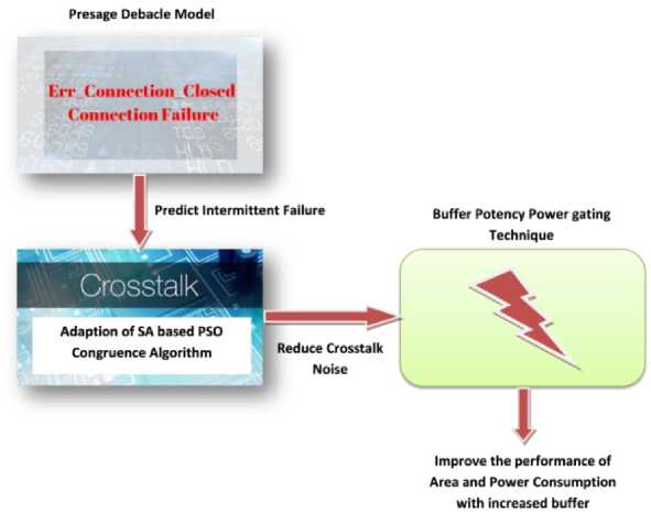
Fig.1. Block Diagram of Proposed Work
Thereafter, the efficiency of the buffer is increased by employing power gating technique which minimizes the overall area and power consumption. To estimate the power gating output and manage the validation of the sleep signal to the buffer inputs, a probabilistic experiment was conducted. Power-gating is a practical method for effectively mitigating NoC power control schemes without any loss in performance. Therefore, the proposed work efficiently handles the intermittent failure, achieves high fault tolerances, and magnificent device performance by improving throughput, area, and energy consumption.
-
3.1. Presage Debacle Model
In this Presage Debacle model, the intermittent failure is predicted by providing real-time application traffic to the application-specific topology. The length of the link in asynchronous NoC (ASNoC) varies depending on how routers are mounted on the chip plane. The reliability of connections present in ASNoC should be addressed properly as the interconnection links are very crucial in data transmission among cores via routers. Due to the effect of Electromigration, Electro-Fault, EMI, and physical damage irreversible connection defects are caused. In order to overcome permanent link failures, effective defect models are also needed. The default value of probability relies on the Mean Time to Failure distribution as given in the equation (1).
с , н
MeanTimeToFailure = —(ект^
Where ‘C’ is the driver’s field, the actual density is ‘J’, ‘H’ represents the activation energy, ‘K’ is Boltzmann constant and ‘T’ depicts the temperature (ambient and joule heating). The equation1, shows that increase in temperature ‘T’ leads to high MTTF thereby increasing the possibility of failure. The distribution was tested using Cadence Virtuoso tool by building an on-chip interconnection wire model. To demonstrate the empirical failure model, experiments were carried out in an application-specific NoC plan for various interconnection link widths. The experiments now have the following technical parameters: 180 nm CMOS technology, supply voltage VDD as 1.8 V, load of 20 fF and length of connection wire as 1 mm. The schematic diagram of the modelled and extracted interconnection component is shown in Fig. 2. The input provided to the fault model is a connectivity prerequisite i.e., Megabit per second bandwidth (Mbps) connecting the application edges and power dissipation across the links.The amount of power dissipated is transformed into heatwhich harms the physicallink.
The traffic among the cores is the input given to the link fault model and is depicted in Fig.3 in the form of a square wave with frequency defined in Hz. The frequency required for sending one-bit data is 1 Hz, and the frequency required for transmitting multi-bit data is 100 MHz, or 100 Mbps. To transmit the four-bit of data [1,0,1,0] via a 1 mm link, a frequency of 2Hz must be supplied as an input for the fault model.
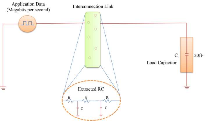
Fig.2. Interconnection link modeled and extracted RC
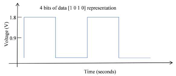
Fig.3. Sample application data pattern
The system traffic for this experiment is represented in combinations of 1s and 0s, 1 corresponding to 1.8V and 0 corresponding to 0V. The amount of power dissipated is evaluated for a 1 mm length interconnection link having width of 0.3µm. The power dissipation for 100 Mbps of data is 0.3µW. The amount of power dissipation corresponding to system traffic rises exponentially and is transformed into heat affecting the link. The equation1 shows that MTTF is inversely related to the current density and temperature. Since dissipation is transformed to temperature, the MTTF decreases as dissipation increases. This illustrates that MTTF decreases in response to high contact demands or BW. This prompted us to study the MTTF for numerous implementations plans in the literature. The appliance traffic is described as a square wave, and the effects of a link in an ASNoC architecture are reported at different bandwidths. This study provides prediction of intermittent failure by sending application traffic to high-bandwidth links in the real application-specific topology. The power dissipation in the output gradually increases and is converted to heat. As power dissipation increases, it produces crosstalk noise as well as high area consumption. To minimize crosstalk noise, an adaptation of the SA-based PSO Congruence Algorithm is used as described below.
-
3.2. Adaption of SA based PSO Congruence Algorithm
The aim of developing a congruence optimization algorithm is to properly map each and every task present in the application program to a specific topology node and to find the best network output. When a task is projected onto the chip network using the congruence algorithm, the relative location of the task is determined. The crosstalk inside the on-chip network is primarily at the point of intersection and the relative location of tasks has a major impact on the contact point. To minimize crosstalk in the network-on-chip, the congruence algorithm has to adapt continuously to the task position in the topology structure. Therefore, the method for changing the task location in the mapping algorithm is critical. The two parts of the congruence algorithm are: Particle swarm optimization and simulated annealing optimization
The essence of particle swarm optimization as a classical heuristic congruence algorithm, is to use the three messages of the current solution, specific best solution, and global best solution to direct particles to optimize and update, among which balancing individual experience and group experience is the key to algorithm optimization.
The various advantages of PSO algorithm include rapid searching speed, increased efficiency and ease of parameter adjustment. It is, however, vulnerable to premature convergence and leads to a locally optimized solution. The algorithm of simulated annealing is very beneficial while finding the best solution locally. It further accepts this degrading solution with some probability which gradually decreases with reduction in temperature. The optimal local solution can be easily avoided by adding the degrading solution. Since the simulated annealing algorithm compensates for the particle swarm optimization algorithm, the two algorithms can be combined in the design of a chip network congruence algorithm. The operating flow of the congruence algorithm adaptation can be summarized in nine phases.
Phase 1: Randomly create some mapping schemes.
Phase 2: Initiate minimal crosstalk and trace each particle optimally. Compare and obtain the minimal historical and global crosstalk along with optimum congruence. Label the optimal particle.
Phase 3: Choose various optimization strategies based on whether the particle is optimum. Slide to phase6 in case it corresponds to the optimal particle, else continue with phase4.
Phase 4: Modify the speed and direction of the particle with respect to the above rules.
Phase 5: Measure each particle's crosstalk noise, update every particle's minimum crosstalk noise, report congruence mode simultaneously and move to phase8.
Phase 6: Swap random congruence positions in the optimal particle for two tasks. If the present value of crosstalk is lower when compared toparticle’s minimum crosstalk, then update the value of particle’s minimum crosstalk and corresponding mapping else revise with a certain probability.
Phase 7: Evaluate if all particles have been modified in the particle swarm. Go to phase9 if yes. Else go to phase3.
Phase 8: Modifyglobal minimal crosstalk noise and congruence mode as well as replenish optimum particles. If the global minimum crosstalk is less than the historical minimum crosstalk, update the historical minimum and historical optimum congruence approaches.
Phase 9: The optimum solution is returned after the iteration. If not, the PSO inertia component ω and the SA temperature parameter t are modified and the phase3 is taken.
Algorithm 1:
Input: Iteration Count: N T, Scale of the population: P T
Factor: Inertia factor: ω, Factor of learning: L 1, L 2 , Random value: M 1 , M 2, Temperature Control: T, Minimum Individual Crosstalk: C I, Minimum Global Crosstalk: C G , PresentIteration Count: N P , Number of particles crossed: PC, Individual Optimal Congruence: OI, Global Optimal Congruence: OG, Present Particle Label: FP, Optimal Particle Label: FO
Output: CH represents Historical minimum crosstalk, OH is Historical optimal Congruence
Procedure:
Randomly generate initial particle swarm mapping solutions;
Compute the crosstalk that fits each congruence particles;
Document the minimum initial crosstalk C I and congruence mode O I ;
By comparison, get global minimum crosstalk C G and globally optimal congruence O G and mark the optimal particle Fo;
Start Historical optimal Congruence OH and Historical minimum crosstalk CH while (Np < NT)
while (Pc < PT)
if (FP==Fo)
Exchange the location of two tasks randomly and calculate the crosstalk;
if (crosstalk < C , )
Update C I and O I ;
else
Update CIand OIbased on the criteria of the metropolis endif else
Update each particle's speed and also position;
Compute particle crosstalk and modify CIand OI endif end
Use comparison to update C G and O G ;
Update C H and O H ;
Modify to and T end return OH
Thus, the above heuristic congruence algorithm improves crosstalk optimization. The combination of Particle Swarm Optimization (PSO) with the Simulated Annealing (SA) algorithm provides a globally optimal solution which is difficult to collapse into a local minimum. This reduces the cross talk of the on-chip network. Once the crosstalk noise is reduced, the efficiency of the buffer is increased by the Buffer Potency Power gating technique which reduces the total area and power consumption.
-
3.3. Buffer Potency Power gating technique
In this technique, the value of total area and power consumption is reduced by emphasizing on modification of virtual channels in the router input ports. A series of flow-through data correction programs, in particular, have been designed for an intensive base structure to minimize changes in operation and changed interconnection behavior. The virtual channel classification field increases the complexity of the communication as it adds more bits to the contents of flits. Data must also be exchanged on a virtual channel basis between nodes. The information related to the state of the virtual channel should be presented to the nodes.The transmission node stores information like the number of free buffers, the virtual channel assignment and the packet priority. The receiver node often has virtual channel assignments, inputs, and outputs for each route buffer and channel.
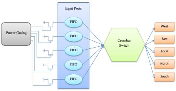
Fig.4. Power Gating Technique
FIFO Versatility Controller: The latest add-on module will determine which FIFOs on the network can hold an incoming packet. Eventually, the output ports must communicate in order to send the received packets to their downstream routers in accordance with the route scheme.
FIFO buffer: The FIFO accepts packets not only from the upstream routers that have been directly linked here as Base FIFO routers, but also from other input ports.
Send logic: use the routing algorithm to determine the packet's direction so that the appropriate output port can be selected. In the event of a conflict, the operation of the portable router is identical to that of the Base router.
For the matter of argument, the Flexible Router is no longer required until one or more free slots are available in the required entire FIFO as with the Base Router. FFC, on the other hand, seeks a free slot in the router in any relevant FIFO that is not full by requiring FIFOs in the other input ports that are not complete, and when a free slot is identified, this returns the application to the upstream path. The packet will then be given to the FIFO chosen. The Stable Router then performs the same functions as the Base Router. For effectual use of power gating, the sleep transistor must be properly sized as it affects the output of all attached gates.A significant one indicates a significant increase in the area for ON/OFF transitions, as the circuit is slowed down by an unacceptable small resistor due to its high resistance. One of the challenges is calculating the accumulated current injected through the sleep transistor drainage-source pathway, which leads to worsening of sleep latency while the process is active, as shown in Fig. 4.
This technique is known as the sleeping cluster insertion, which is a solution that connects many cell subsets, or clusters, with dedicated transistors in the overall organized sleep network. To increase the efficiency of the system, the sleep transistor must be properly designed. Furthermore, a small sleep transistor can slow the active circuit because of its high power. Thus, a larger circuit needs a wide area of operation and significant driving energy cost. In general, designers set a threshold for IR drops (for example, 10% VDD) to meet a sleep resistance scale transistor. The average sleep channel resistance can be determined using equation (2).
VDD av α
ION
While the VDD remainder of the sleep transistor will lower the voltage as a proportion of the voltage supply and the ION represents the highest discharge current. In the active mode, cells with power gatingare injected into the sleep transistor. The active current is difficult to calculate. An inaccurate ION approximation indicatesa sleep transistor size that is too small, potentially increases area, power and can also lead to timing infringements in active mode of operation. The sleep transistor operates in a stable region and its size must be precisely determined. Traditional flow control methods like wormhole routing performs allocation of buffer first to prevent it from moving the current node away when the flit is returned and to alert the current node about availability of buffer.
Once the turn-around time is met, the buffer is available for reuse. The valid turn-around time associated with the buffer should be no less than the amount of the delay involved in transmitting the data flit towards the forward direction andreceiving the flow control back. The approach described in the paper optimizes the overall buffer. The complex distribution related to these buffers on multiple virtual channels should be examined. It will also improve buffer utilization since the buffering requirement is different for all virtual channels. The development of complex virtual networks provides a simple framework for various schemes. It is more difficult to assign a buffer to virtual channels dynamically and thus increases the complexity of the design. The aim of these dynamic systems is to optimizethe buffer output. This increases the buffer's performance while decreasing its area and power consumption while maintaining optimum throughput and low latency.
Thus, from the overall methodology, it is clearly shown that the area and power consumption is improved along with reduction in crosstalk noise and prediction of intermittent failure. By providing real traffic in the applicationspecific topology, the presage debacle technique predicts intermittent failure in the application link. The power dissipates in the output and is converted to heat by the joules heating method while predicting the failure. This leads to increased crosstalk noise, high area and power consumption. The adaptation of the SA-based PSO congruence algorithm is designed to overcome the crosstalk noise. The mapping algorithm must continuously change the task location in the topology structure, which progressively reduces network-on-chip crosstalk. Then there's Buffer Potency. The power gating technique increases the buffer efficiency while reducing area and power consumption.
4. Results and Discussion
In this section, the experimental setup for testing the proposed solution is presented. The results are then compared with the previous methods to illustrate the efficiency of the proposed method. The simulation is performed using Xilinx ISE.
-
4.1. Simulation Output
Fig.5 shows the block level schematic of proposed method.
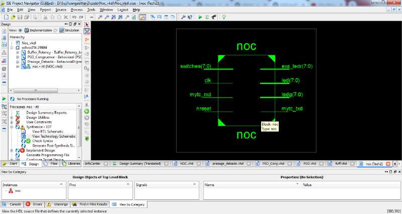
Fig.5. Illustration of simulation design
Fig.6., shows the input given to the proposed method. This processuses three models: Presage Debacle Model, Hybrid congruence algorithm and buffer potency to enhance the performance of the system and also decrease area and power consumption. Delay and dissipation of power on the wire line are achieved by cadence simulations based on the NoC topology which takes into account the unique lengths of each connection.
Table 1. Device utilization Summary
|
Logic utilization |
Used |
Available |
Utilization |
|
Number of slice registers |
2101 |
93120 |
2% |
|
Number of slice LUTs |
3523 |
46560 |
7% |
|
Number fully used LUT-FF pairs |
2099 |
3525 |
59% |
|
Number of bonded IOBs |
36 |
240 |
15% |
|
Number of BUFG/BUFGCTRLs |
1 |
32 |
3% |

Fig.6. Simulation input of the NoC Model
The Table 1. describes the device utilization summary and shows the utilized slice registers, slice LUTs, LUT-FF pairs, Bonded IOBs and BUFG/BUFGCTRLs whose corresponding values are 2101, 3523, 2099, 36 and 1 presenting the, utilization percentage of 2%, 7%, 59%, 15% and 3% respectively.
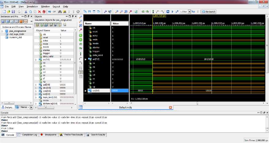
Fig.7. Simulation output of Presage Debacle Model
Fig. 7., shows the output of the proposed presage debacle model. In this model, intermittent failure is predicted for high-bandwidth links in the application-specific topology. The model's output is power, which is dissipated and converted to heat. Crosstalk noises are generated as a result of power dissipation and have a high area and power consumption. The primary goal of implementing the novel algorithm is to reduce the model's crosstalk noise. The congruence algorithm continuously changes the task location in the topology structure, steadily reducing crosstalk of the network-on-chip. The proposed technique is intended to minimize the area and power dissipation by altering the virtual channels in the router's input ports that connects the network to the chip along with the routers and network interfaces. This increases buffer performance while maintaining optimum throughput and low latency.
-
4.2. Comparison Output
In evaluating the performance of thePresage Debacle Model on Network-on-Chip (NoC), compare the evaluation results with three states of the art algorithms, such as Transient Error Code (TEC) [21], Hamming Product Code (HPC) [22], and MECCRLB [23].
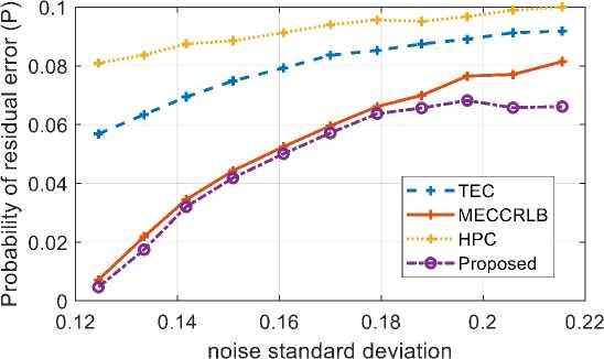
Fig.8. Comparison of Probability residual error in terms of noise standard deviation
Fig. 8 depicts the comparison between proposed approach and existing methods like TEC, HPC, and MECCRLB respectively in terms of probability of residual error. The proposed method has less error rate when compared to the existing methods. The proposed method obtains lesser crosstalk noise with approximately 0.06 residual errors which lower than the existing methods.
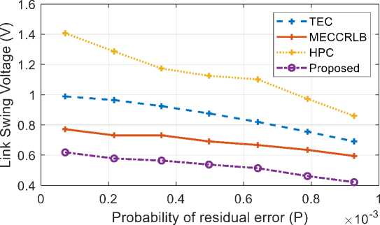
Fig.9. Comparison of Link voltage in terms of residual error
Fig. 9 presents the comparison between proposed approach and existing methods like TEC, HPC, and MECCRLB respectively in terms of Link Swing Voltage. The graph showsclearly that the proposed techniques have a lower voltage in comparison to other existing approaches for all probability of residual error thus producing a high bit error rate. It also illustrates that for example at a particular residual error of 10-3, the proposed voltage is 0.55V. However, for TEC, MECCRLB and HPC, it is 1V, 0.76V and 1.4V respectively.
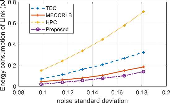
Fig.10. Comparison of proposed with existing methods
Fig. 10 shows the comparison between proposed approach and existing methods like TEC, HPC, and MECCRLB respectively in terms of energy consumption of link with respect to noise standard deviation. It has been discovered that environments with high noise possess high energy consumption. At noise level 0.17, the energy used by the proposed method is reduced by 52% as compared to other existing methods. This shows that the proposed coding scheme saves power and energy by supporting the same amount of error corrections with less connection width as compared to other existing methods.
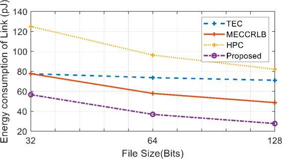
Fig.11. Comparison of Power consumption in terms of file size
Fig. 11., shows the comparison between the proposed method and other existing methods such as TEC, HPC, and MECCRLB respectively in terms of energy consumption. The energy consumption decreases with increasing file size, as seen in the graph. The proposed method consumes 58PJ of energy at 32bits, 38PJ at 64bits, and 30PJ at 128bits which are less than the other state-of-the-art methodologies. Overall, the proposed method has lower voltage, area, and energy consumption than previous techniques such as TEC, HPC, and MECCRLB.
5. Conclusion
One of the important factors gaining prominence in the design of multicore processors with on-chip packet networks, also known as networks on chip (NoCs) is its survival capability. The work proposed a new augur intermittent failure in Network on Chip that predicts the intermittent failure and improves area and power consumption.The Presage Debacle model predicted the intermittent failure in the application-specific topology by providing a real-time traffic to the links. The prediction of link failure during runtime helps to improve the reliability of the system. Also, the crosstalk noise is reduced by the Adaption of SA based PSO congruence algorithm. The crosstalk noise is gradually decreased by continually changing the task position in the topology. Furthermore, the Buffer Potency Power Gating technique reduces the area occupancy and power consumption. A probabilistic experiment is performed to approximate the power gating output and to manage the validation of the sleep signal to the buffer inputs without any loss in performance. The proposed approach reduces area and power consumption by 52%, which is less than the other existing methods such as TEC, HPC, and MECCRLB. Thus, the proposed method enhanced the performance of the system and also achieved improved bandwidth, throughput, and latency. The result obtained from the proposed Prediction of Intermittent Failure by Presage Debacle Model in Network on Chip are less crosstalk of 0.06 residual errors, high BER with minimum link swing voltage of 0.55 V and low energy consumption of 0.17 pj . In future, proposed approach will be extended to investigate the dynamic behavior of MTTF when connection lengths vary as well as for numerous apps running at the same time.
References Prediction of Intermittent Failure by Presage Debacle Model in Network on Chip
- N. L. Venkataraman, and R. Kumar, “Design and analysis of application-specific network on chip for reliable custom topology,” Computer Networks, vol. 158, pp. 69-76, 2019.
- Sangeeta Singh, et. al., “Power and Area Calibration of Switch Arbiter for High Speed Switch Control and Scheduling in Network-on-Chip,” In IEEE 13th International SoC Design Conference (ISOCC), pp. 5-6, 2016.
- S. Paul, N. Chatterjee, and P. Ghosal, “A permanent fault-tolerant dynamic task allocation approach for Network-on-Chip based multicore systems,” Journal of Systems Architecture, vol. 97, pp. 287-303, 2019.
- R. Poovendran, and S. Sumathi, “An area‐efficient low‐power SCM topology for high-performance network‐on Chip (NoC) architecture using an optimized routing design,” Concurrency and Computation: Practice and Experience, vol. 31, no. 14, pp. e4760, 2019.
- P. Kullu, and S. Tosun, “Energy-aware and fault-tolerant custom topology design method for network-on-chips,” Nano Communication Networks, vol. 19, pp. 54-66, 2019.
- C. L. Li, J. C. Yoo, and T. H. Han, “Energy-efficient custom topology-based dynamic voltage-frequency island-enabled network-on-chip design,” Journal Of Semiconductor Technology And Science, vol. 18, no. 3, pp. 352-359, 2018.
- C. H. U. Zhuqin, L. I. Hui, G. U. Huaxi, and Y.E. Xiaochun, “Wavelength assignment method based on ACO to reduce crosstalk for ring-based optical network-on-chip,” Microprocessors and Microsystems, vol. 71, pp. 102849, 2019.
- B. Subramaniam, S. Muthusamy, and G. Gengavel, “Crosstalk minimization in the network on chip (NoC) links with dual binary-weighted code CODEC,” Journal of Ambient Intelligence and Humanized Computing, pp. 1-6, 2020.
- A. Jedidi, “Detection and Monitoring Intra/Inter Crosstalk in Optical Network on Chip,” International Journal of Electrical and Computer Engineering, vol. 8, no. 6, pp. 4912, 2018.
- H. A. M. Harb, et al., “A Study of the Number of Wavelengths Impact in the Optical Burst Switching Core Node,” Proceeding of the Electrical Engineering Computer Science and Informatics, pp. 664-667, 2017.
- L. H. Duong, P. Yang, Z. Wang, Y. S. Chang, J. Xu, Z. Wang, and X. Chen, “Crosstalk noise reduction through adaptive power control in inter/intra-chip optical networks,” IEEE Transactions on Computer-Aided Design of Integrated Circuits and Systems, vol. 38, no. 1, pp. 43-56, 2018.
- N. Chatterjee, P. Mukherjee, and S. Chattopadhyay, “Reliability-aware application mapping onto mesh-based Network-on-Chip,” Integration, vol. 62, pp. 92-113, 2018.
- N. K. R. Beechu, V. M. Harishchandra, and N. K. Y. Balachandra, “Energy-aware and reliability-aware mapping for NoC-based architectures,” Wireless Personal Communications, vol. 100, no. 2, pp. 213-225, 2018.
- W. Gao, Z. Qian, and P. Zhou, “Reliability-and performance-driven mapping for regular 3D NoCs using a novel latency model and Simulated Allocation,” Integration, vol. 65, pp. 351-361, 2019.
- M. G. Moghaddam, and C. Ababei, “Dynamic lifetime reliability management for chip multiprocessors,” IEEE Transactions on Multi-Scale Computing Systems, vol. 4, no. 4, pp. 952-958, 2018.
- L. Daoud, and N. Rafla, “Runtime Packet-Dropping Detection of Faulty Nodes in Network-on-Chip,” In 2019 32nd IEEE International System-on-Chip Conference (SOCC), pp. 266-271, 2019.
- B. Bhowmik, S. Biswas, J. K. Deka, and B. B. Bhattacharya, “Reliability-aware test methodology for detecting short-channel faults in on-chip networks,” IEEE Transactions on Very Large Scale Integration (VLSI) Systems, vol. 26, no. 6, pp. 1026-1039, 2018.
- A. Rodríguez-Ramos, A. J. da Silva Neto, and O. Llanes-Santiago, “An approach to fault diagnosis with online detection of novel faults using fuzzy clustering tools,” Expert Systems with Applications, vol. 113, pp. 200-212, 2018.
- M. H. Moaiyeri, F. Sabetzadeh, and S. Angizi, “An efficient majority-based compressor for approximate computing in the nano era,” Microsystem Technologies, vol. 24, no. 3, pp. 1589-1601, 2018.
- S. Velayudham, S. Rajagopal, Y. V. R. Rao, and S. B. Ko, “Power-efficient error correction coding for on-chip interconnection links,” IET Computers & Digital Techniques, vol. 14, no. 6, pp. 299-312, 2020.
- M. Vinodhini, N. S. Murty and T. K. Ramesh, “Transient Error Correction Coding Scheme for Reliable Low Power Data Link Layer in NoC,” IEEE Access, vol. 8, pp. 174614-174628, 2020.
- A. K. Chlaab, W. N. Flayyih, and F. Z. Rokhani, “Lightweight hamming product code based multiple bit error correction coding scheme using shared resources for on-chip interconnects,” Bulletin of Electrical Engineering and Informatics, vol. 9, no. 5, pp. 1979-1989, 2020.
- M. Vinodhini, and N. S. Murty, “Reliable low power NoCinterconnects,” Microprocessors and Microsystems, vol. 57, pp. 15-22, 2018.
- Javed, Aqib, et al. "Exploring spiking neural networks for prediction of traffic congestion in networks-on-chip." 2020 IEEE International Symposium on Circuits and Systems (ISCAS). IEEE, 2020.
- Wang, Ke, and Ahmed Louri. "Cure: A high-performance, low-power, and reliable network-on-chip design using reinforcement learning." IEEE Transactions on Parallel and Distributed Systems 31.9 (2020): 2125-2138.
- Amin, W., Hussain, F., Anjum, S., Khan, S., Baloch, N.K., Nain, Z. and Kim, S.W., 2020. Performance evaluation of application mapping approaches for network-on-chip designs. IEEE Access, 8, pp.63607-63631.
- Bhanu, P. Veda, and J. Soumya. "Fault-tolerant application mapping on mesh-of-tree based network-on-chip." Journal of Systems Architecture 116 (2021): 102026.
