Progress in research on the technology of obtaining inorganic oxide semiconductors from type P copper (I) oxide
 oxide")
Author: Ren Bingbing, Mindrov Konstantin
Journal: Бюллетень науки и практики @bulletennauki
Section: Технические науки
Article in issue: 8 т.8, 2022.
Free access
As a representative intrinsic type P inorganic semiconductor material, copper (I) oxide Cu2O has been widely used in photovoltaic, catalysis, chemical industries and other fields, and has an extremely important position. For a long time, the literature on the preparation method and preparation technology of Cu2O is relatively scattered and independent, resulting in a certain degree of obstacles and difficulty in obtaining relevant technical knowledge and understanding its internal principles. Aiming at the progress and innovation of Cu2O preparation methods and technology in recent years, combined with the team’s long-term experience accumulation and research results, this article focuses on the classification, principles and characteristics of Cu2O preparation methods, and the optimization methods and development directions of Cu2O preparation technology. The outlook was carried out. This review aims to provide reference and guidance for the preparation and research of Cu2O and other related inorganic oxide semiconductors.
Copper (i) oxide, inorganic oxide, type p semiconductor
Short address: https://sciup.org/14125294
IDR: 14125294 | UDC: 538.955 | DOI: 10.33619/2414-2948/81/26
Прогресс в исследованиях технологии получения неорганических оксидных полупроводников из оксида меди (I) типа P
В качестве репрезентативного неорганического полупроводникового материала типа P оксид меди (I) Cu2O широко используется в фотоэлектрической, катализной, химической промышленности и других областях и занимает чрезвычайно важное положение. Долгое время литература по способу получения и технологии получения Cu2O была относительно разрозненной и независимой, что приводило к определенной степени препятствий и трудностей в получении соответствующих технических знаний и понимании ее внутренних принципов. Стремясь к прогрессу и инновациям в методах и технологиях получения Cu2O за последние годы в сочетании с накоплением многолетнего опыта команды и результатами исследований, эта статья посвящена классификации, принципам и характеристикам методов получения Cu2O, а также методам оптимизации и направлениям развития технологии получения Cu2O. Прогноз был выполнен. Цель этого обзора - предоставить справочные материалы и рекомендации по получению и исследованию Cu2O и других связанных с ними неорганических оксидных полупроводников.
Text of the scientific article Progress in research on the technology of obtaining inorganic oxide semiconductors from type P copper (I) oxide
Бюллетень науки и практики / Bulletin of Science and Practice Т. 8. №8. 2022
UDC 538.955
Бюллетень науки и практики / Bulletin of Science and Practice Т. 8. №8. 2022
In nature, most inorganic oxide semiconductor materials show intrinsic n-type semiconductor properties, such as n-TiO 2 , n-ZnO, n-wo 3 and n-fe 2 o 3 [1-4]. There are oxygen ion vacancies in their crystal structures, which contain free moving electrons. In contrast, a few inorganic oxides represented by cuprous oxide (Cu 2 O) have metal ion (copper ion) vacancies, which show the intrinsic p-type semiconductor characteristics, namely hole transport characteristics. Due to the increasingly prominent importance of p-type oxide semiconductors in the fields of energy and materials, and the number of p-type oxides that can be selected is very rare compared with that of n-type oxides, Cu 2 O, as a representative p-type oxide among them, has attracted much attention in many research fields [57]. Human beings are not unfamiliar with Cu 2 O. As early as 1926, Cu 2 O was applied to rectifier diodes [8]. In 1930, Schottky put forward the theory of "photovoltaic effect" based on Cu 2 O barrier [9]. In modern times, Cu 2 O has been widely involved in the fields of photovoltaic and photocatalysis and has become a "guest" of light energy conversion materials.
As a traditional inorganic oxide semiconductor material with a long history, the previous literature has introduced and summarized the preparation methods of Cu 2 O to a certain extent, but the content is relatively scattered and independent, and the explanation of the process and mechanism is relatively brief. This research group has been studying the synthesis, preparation and research of Cu 2 O materials for more than ten years. This paper will systematically classify, summarize and summarize a wide variety of Cu 2 O preparation methods, and deeply analyze various technical schemes, in order to enlighten and help the related research of Cu 2 O.
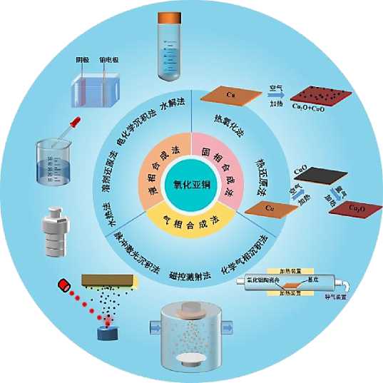
Figure 1. Classification and schematic diagram of the preparation methods of cuprous oxide
Thermooxidationmethod is the simplest Cu 2 O synthesis method. As the name suggests, this method takes copper as raw material and oxidizes copper in an aerobic environment, in order to convert copper into Cu 2 O in one step, as shown in Formula 1. However, because it is difficult to accurately control the oxidation degree of copper, it is usually accompanied by the formation of copper oxide (CuO) (formula 2). A. O. Musa et al. [10] analyzed and studied the oxidation process and products of copper in air atmosphere. It was found that below 1040 ℃, the oxidation product of
Бюллетень науки и практики / Bulletin of Science and Practice Т. 8. №8. 2022 copper was a mixture of CuO and Cu2O. The emergence of CuO could be avoided as much as possible only when the oxidation temperature was controlled above 1050 ℃. 10. Hong et al. [11] reported that copper nanowires synthesized by polyvinyl pyrrolidone (PVP) template method can be spontaneously oxidized to Cu2O nanowires at room temperature, with a diameter of about 10nm. However, this method is not suitable for other copper substrates, so it is difficult to popularize. It is not difficult to see that although the thermal oxidation method has low requirements for equipment, simple steps and high output, the one-step oxidation of copper to Cu2O in air atmosphere is still a relatively extensive chemical process. It is not only easy to generate Cu2O in the heating and cooling stages, but also the subsequent process often requires pickling and etching to obtain relatively pure Cu2O.
△
4Cu+O 2 ^ 2Cu 2 O
2Cu+O 2 Д 2CuO (2)
In order to avoid the complex reaction path of copper in the thermal oxidation method, our research group developed the thermal reduction method to complete the preparation of high-purity Cu 2 O [12]. Unlike the thermal oxidation method, which uses copper as raw material, the thermal reduction method uses CuO as raw material and uses the reducibility of metal copper to reduce CuO to Cu 2 O, that is, at high temperature, copper is used to reduce CuO and react to produce Cu 2 O (formula 3). In the specific operation, our research group first takes the metal copper as the substrate, calcines the surface layer of the copper substrate under the air atmosphere to produce CuO with a certain thickness, and then anneals at high temperature in an inert atmosphere (such as argon and nitrogen). At this time, the inner copper atom gradually reduces the surface layer CuO to Cu 2 O. When the annealing temperature reaches more than 700 ℃, CuO is fully reduced to obtain a high-purity Cu 2 O film (Figure 2). In other embodiments, Luo et al. [13] first oxidized the surface of the copper substrate to form copper hydroxide (Cu (OH) 2 ) nanowires by electrochemical oxidation, and then transformed the copper hydroxide nanowires into Cu 2 O nanowires by thermal reduction reaction in an inert atmosphere (Figure 3).
△
Cu+CuO ^ Cu2O
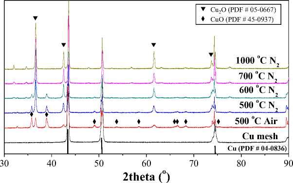
Figure 2. X-ray diffraction spectra of cuprous oxide changed with temperature in thermal reduction method [12]
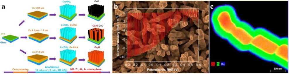
Figure 3. (a) Synthesis schematic diagram of Cu 2 O nanowire arrays prepared by thermal reduction method [13]; (b) SEM images and photocurrent curves of Cu 2 O nanowire arrays prepared by thermal reduction method [13]; (c) EDX spectra of multilayer composite Cu 2 O nanowire arrays prepared by thermal reduction method [13]
Chemical vapor deposition (CVD) is a process in which the substrate is exposed to one or several precursor atmospheres, and the precursor reacts on the surface of the substrate to produce the target product. H. Kobayashi et al. [14] used chemical vapor deposition to supply the precursor Cui to the reactor growth zone at 883k with cuprous iodide (Cui) as the precursor and N 2 as the carrier gas. Finally, Cu 2 O thin films with a band gap of 2.38ev and high crystallinity were grown on single crystal mgo {110} substrates. H. Kim et al. [15] reported that the hall mobility of Cu 2 O thin films prepared by atomic layer deposition using a fluorine-free amino alkoxide precursor can reach 8.05cm2v-1s-1. Atomic force microscopy (AFM) was used to analyze the roughness of Cu 2 O films deposited by atomic layers at different growth temperatures. The results showed that the roughness of Cu 2 O films increased with the increase of temperature (Figure 4).
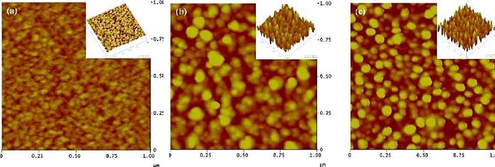
Figure 4. Atomic force microscopy (AFM) of Cu 2 O films by atomic layer deposition at different deposition temperatures: (a) 140 ℃, (b) 180 ℃, (c) 240 ℃ [15]
Magnetron sputtering technology is the most widely used vacuum coating technology in industry at present. It has significant technical advantages and can be used for the preparation of all thin film materials; Moreover, the prepared film material has high density, few pinholes and good repeatability. The chemical composition of the film can be adjusted by adjusting the composition of the target material. When preparing Cu 2 O thin films by magnetron sputtering, there are many solutions. Reactive sputtering can be carried out with copper as the target and oxygen as the reaction gas (Formula 1) [16]. Or use CuO ceramic target for reactive sputtering; Cu 2 O target can also be directly used for direct sputtering. Y. S. Lee et al. [17] prepared Cu 2 O semiconductor films by reactive
DC magnetron sputtering on quartz substrates with metal copper targets and used the method of controlling the substrate temperature and changing the reaction atmosphere flow rate ratio (AR ∶ O 2 ) to regulate the grain size and phase purity of Cu 2 O films. The results showed that the grain size gradually increased with the increase of substrate temperature (Figure 5). Similarly, K. K. Markose et al. [18] prepared Cu 2 O thin films on the surface of monocrystalline silicon by RF magnetron sputtering with copper as the target, oxygen as the reaction gas and argon as the sputtering gas. S. Noda [19] directly used sintered Cu 2 O and CuO ceramic targets to prepare Cu 2 O films by adjusting the flow rate ratio of oxygen and argon during magnetron sputtering and controlled the crystalline phase of the films. After high temperature annealing, the hall mobility of Cu 2 O films was 16.6cm2v-1s-1, and the carrier concentration was 3.5 × 1015cm-3
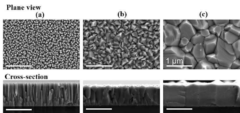
Figure 5. SEM images of Cu 2 O films deposited by reactive direct current magnetron sputtering, with growth temperatures of (a) 300 K, (b) 600 K, and (c) 1070 K [17]
Pulsed laser deposition (PLD) is widely used in laboratory research at present. It also benefits from its wide range of materials, easy adjustment of target element components, and high film forming quality. In 2003, m. ivill et al. [20] used pulsed laser deposition technology (Mn doped Cu 2 O target, KrF excimer laser, 5Hz laser frequency, laser pulse energy density of 1~3j\/cm2) to prepare Mn doped Cu 2 O thin films with high conductivity on single crystal MgO substrate. S. Lee [21] using KrF excimer laser ( λ= 248nm) and CuO ceramic targets. By changing the absorbed atomic energy and flux of laser pulses, it was found that Cu 2 O nanostructures with different crystal plane orientations and geometric shapes could be grown on the surface of strontium titanate (SrTiO 3 , STO) substrates with different orientations (Figure 7). In 2009, chen [22] prepared Cu 2 O polycrystalline thin films on si {100} substrates by pulsed laser deposition. The results show that with the increase of oxygen partial pressure, the structure of the film gradually changes from Cu 2 O to CuO (the critical value of oxygen partial pressure is 0.4pa) (Figure 6). 10. H. Liu et al. [23] reported the technology of depositing single crystal Cu 2 O thin films on mgo {110} substrates by pulsed laser deposition, and studied the effect of deposition oxygen partial pressure on the structure and properties of the films. The results showed that pure Cu 2 O with high crystallinity and high transmittance was prepared when the oxygen partial pressure was 0.09pa. The single crystal Cu 2 O films deposited under the optimum conditions showed excellent carrier mobility (23.75cm2v-1s-1) and carrier concentration (3.94 × 1016cm-3) and extremely low resistivity (6.67 Ω cm).
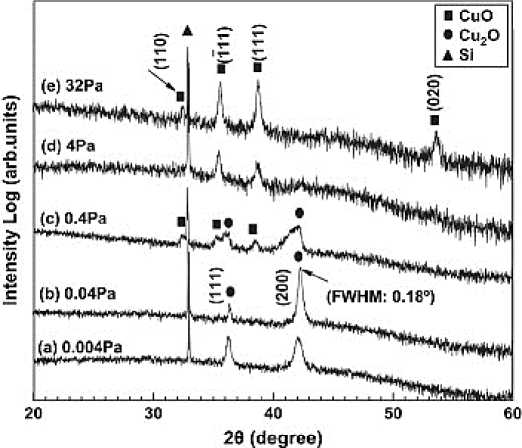
Figure 6. XRD patterns of Cu 2 O films by pulsed laser deposition at 500 ℃. The oxygen pressure is: (a) 0.004 Pa, (b) 0.04 Pa, (c) 0.4 Pa, (d) 4 Pa and (e) 32 Pa, respectively [22]
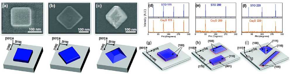
Figure 7. SEM images and epitaxial diagrams of Cu 2 O nanostructures prepared by pulsed laser deposition. (a-c) Deposition on STO{001} substrate at 700 ℃, the laser fluence is: (a)0.78 J/cm2, (b)0.59 J/cm2, (c)0.39 J/cm2[21], (d-f) The φ-scanning atlases of substrate. The substrate is: (d) STO {001}, (e) STO {110}, (f)STO{111}[21], (g-i) Nanostructure and epitaxy of Cu 2 O prepared on different substrates by pulsed laser deposition. The substrate is: (g) STO {001}, (h) STO {110}, (i) STO {111}[21]
Hydrothermal method generally uses water as solvent to grow crystals under high temperature and high pressure in a closed pressure vessel. If water is replaced by organic solvent, it is called solvothermal method. 50. F. Guo et al. [24] first reported the hydrothermal synthesis of Cu 2 O nano cubes with hollow cubic structure. Through hydrothermal synthesis, our research group also realized the growth of Cu 2 O single crystals that simultaneously exposed three crystal planes {100}, {110}, and {111} (Figure 8), and systematically studied the physical and chemical characteristics of each crystal plane of Cu 2 O single crystal. The experiment found that the deactivation of Cu 2 O single crystal was not a one-step deactivation previously inferred, but a two-step deactivation process of oxidation before reduction, which provided a theoretical basis for the study of photocatalysis of single crystal Cu 2 O [25].
Solvent reduction method is the most used method to prepare Cu 2 O powder materials. It has the advantages of low cost, simple process and high purity. This method generally uses soluble divalent copper salts (such as CuCl 2 , CuSO 4 , Cu (NO 3 ) 2 , etc.) as raw materials to react with reducing agents to reduce divalent copper to monovalent copper. Common reducing agents include hydroxylamine, hydrazine hydrate, formaldehyde, etc. In the chemical experiment class in high
Бюллетень науки и практики / Bulletin of Science and Practice Т. 8. №8. 2022 school,we experienced the process of glucose reducing copper hydroxide to produce Cu2O. Similarly, M. Z. Wei et al. [26] dissolved CuSO4 5H2O and NaOH in deionized water and stirred them until they were fully mixed. At the same time, ethanol was added as reducing agent and solvent. After heat treatment at 140 °C, CU2O nanorods with different aspect ratios were successfully prepared. C. S. Tan et al. [27] dissolved cu2+ in aqueous solution containing surfactant and used hydroxylamine and glucose as reductants to prepare Cu2O single crystal particles with specific morphology.
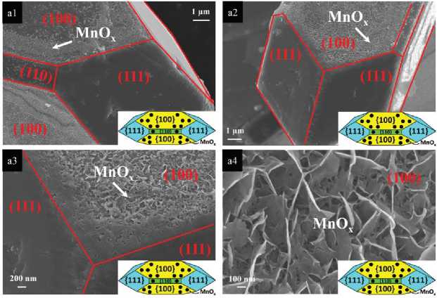
Figure 8. SEM images of the cuprous oxide single crystal particles prepared by hydrothermal synthesis and MnO x photo-deposition [25]
Hydrolysismethod is a method that takes univalent copper compounds (such as CuCl , CuAc , Cu 2 SO 4 , etc.) as reactants to obtain Cu 2 O through hydrolysis reaction. H. Liu et al. [28] used hydrolysis method according to the characteristics of different reactions of CuCl in water with different pH values (i. e. complexing at low pH values (pH˂2.4) and disproportionation (2.4˂pH˂5.0), alkaline hydrolysis reaction occurs when ph>5.0), and uniform hollow Cu 2 O nano cubes are prepared (Figure 9). Other reactants include sodium sulfite, sodium phosphate, etc. after the reaction, the suspension of Cu 2 O is obtained, and then the product is obtained by centrifugation and drying. This method is only applicable to powder materials, and the obtained Cu 2 O has uniform grain size and high yield.
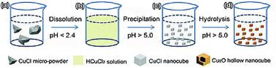
Figure 9. Schematic illustration of the hydrolysis synthetic route from CuCl micro-powder to fine hollow Cu 2 O NCs with uniform sizes [28]
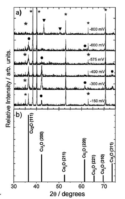
Figure 10. (a) XRD patterns for Cu 2 O films electrochemically deposited under different applied potentials at 30 °Cand pH=9: CU 2 O ( • ), metallic Cu ( ▼ ), and Ti substrate ( ★ ). (b) Reflections of CU 2 O according to the JCPS card (78-2076) [32]
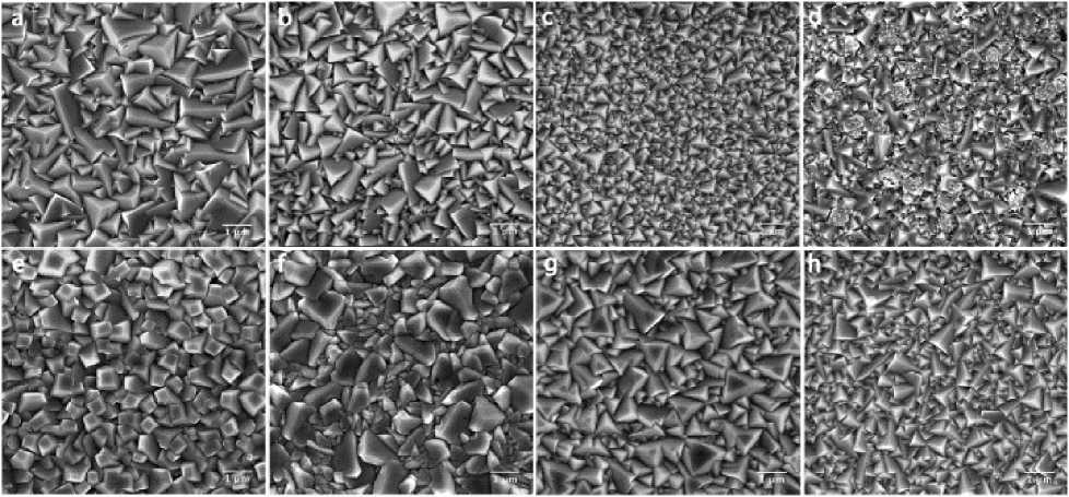
Figure 11. SEM images of Cu 2 O films deposited from the copper lactate solution buffered at pH=12. (a)~(d) At 30 ℃ for deposition currents of -0.05, -0.1, -0.15, -0.2 mA cm-2, respectively; (e)~(h) At 60 ℃ for deposition currents of -0.2, -0.4, -0.8, -1.6 mA cm-2, respectively [34]
In addition, the research group used the two-electrode method to study the electrochemical deposition of Cu 2 O. It was found that when the voltage was controlled in the appropriate range (1.0~1.5v), high-quality Cu 2 O single crystal films could be grown in situ by electrochemical deposition. The SEM image shown in Figure 12a-g shows the growth process of single crystal thin film. From the Figure, we can observe that in the initial stage (0-5min), the regular top up Cu 2 O nano cube is highly dispersed on the substrate, and its grain size increases with the extension of deposition time. After electrochemical deposition for 10 minutes, the size of the nano cube increased to about 300nm, and most of the nano cubes were interspersed with each other. At the same time, a layer-bylayer growth mode was observed. Finally, the grown nano cubes were combined to form a dense single crystal film, and many triangular pyramid structures were displayed on the surface. Each triangular pyramid exposed three {100} crystal planes, as shown in the simulated three-dimensional crystal structure diagram (Figure 12h) [37]. High-quality electrochemical growth can also regulate the exposed crystal surface, and then obtain Cu 2 O single crystal films with different crystal exposed surfaces on both sides (Figure 13a)
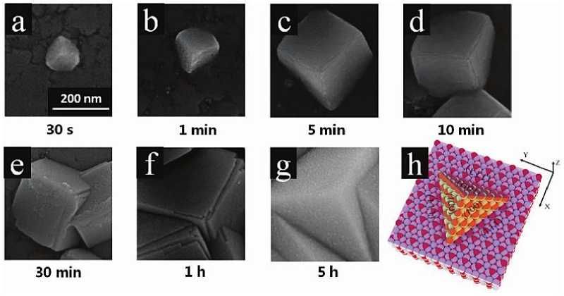
Figure 12. (a-g) SEM images of the growth process of the Cu 2 O single crystal film over time; (h) Schematic plot of the orientated growth of the Cu 2 O single crystal film along the z-axis [37]
The surface of Cu 2 O single crystal films grown under strong alkaline conditions is covered by {100} crystal planes, and the back is composed of {111} crystal planes. From the cross-sectional SEM photos (Figure 13b), it can be observed that the Cu 2 O single crystal film obtained by this technology is uniform and dense inside, showing the characteristics of less grain boundaries and fewer defects. At the same time, this Cu 2 O single crystal film with crystal plane anisotropy grown by electrochemical deposition has the characteristics of carrier self separation compared with the Cu 2 O single crystal film with crystal plane anisotropy, and has the potential to use both thermal energy and light energy (Fig. 13c-d). In the subsequent research, according to the mechanism of Cu 2 O single crystal film (deactivation results from the contact between Cu 2 O and protons), our research group proposed that the selection of protective layer must be dense to isolate protons on the one hand, and conducive to electron conduction to complete carrier transport on the other hand. Therefore, in the follow-up study, the Ag film (10nm) deposited by polyurethane acrylate (PUA) and high-power pulsed magnetron sputtering (hipims) were used to form a dense proton isolation layer, which inhibited the deactivation of Cu 2 O single crystal film [35, 36].
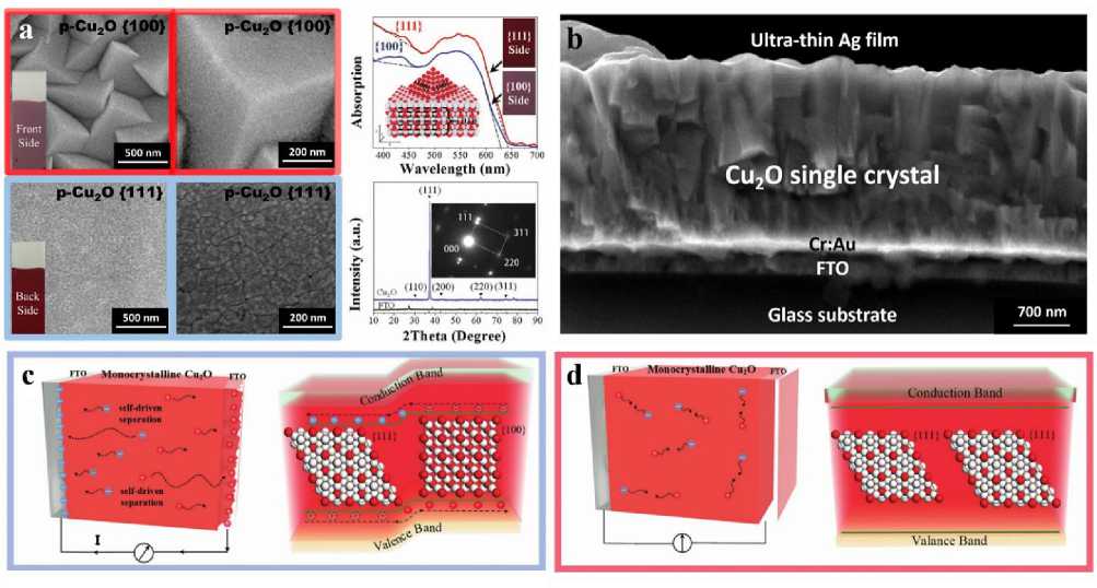
Figure 13. (a) SEM images, front view (Cu 2 O{100} crystal plane) and back view (Cu 2 O{111} crystal plane), diffuse reflection UV-vis absorption spectra and X-ray diffraction spectra of Cu 2 O single crystal films with anisotropic crystal facet unit grown by electrodeposition [37]; (b) SEM images of cross-section of Cu 2 O single crystal films with anisotropic crystal facet unit grown by electrodeposition [36]; (c) Schematic plots of the Cu 2 O single crystal films with anisotropic crystal facet unit grown by electrochemical deposition and the corresponding band structure [37]; (d) Schematic plots of the Cu 2 O single crystal films with two homogeneous crystal faces and the corresponding band structure [37]
The preparation methods of Cu 2 O continue to develop and mature, which can be divided into solid-phase synthesis, gas-phase synthesis and liquid-phase synthesis. Thin film and monocrystallization of Cu 2 O are the most obvious development trends. Thin film means that Cu 2 O can be standardized and prepared in large size. Single crystal can make the internal crystals of the film perfectly arranged and reduce grain boundaries and crystal defects. Exploring the preparation technology with high film forming quality and controllable exposure of crystal surface will become the research focus of Cu 2 O preparation technology. In addition, the research and development of Cu 2 O also has the trend of functionalization and low cost. For example, the development of Cu 2 O single crystal films with high hole transmission performance by low-cost electrochemical deposition has great application potential in the field of heterojunction photovoltaic devices.
To sum up, it is believed that with the continuous efforts of scientific researchers and the continuous exploration of growth mechanism and synthesis methods, the corresponding new efficient and stable Cu 2 O will become a semiconductor material with good performance and wide application, and will eventually be put into practical application, serving the fields of photocatalytic decomposition of water to produce hydrogen, reduction of carbon dioxide, hole transport materials for solar cells, biosensors, catalytic degradation, semiconductor functional devices and so on, Make great contributions to the progress of human society.
Бюллетень науки и практики / Bulletin of Science and Practice Т. 8. №8. 2022
References Progress in research on the technology of obtaining inorganic oxide semiconductors from type P copper (I) oxide
- Khan, S. U., Al-Shahry, M., & Ingler Jr, W. B. (2002). Efficient photochemical water splitting by a chemically modified n-TiO2. Science, 297(5590), 2243-2245. https://doi.org/10.1126/science.1075035
- Shim, M., & Guyot-Sionnest, P. (2001). Organic-capped ZnO nanocrystals: synthesis and n-type character. Journal of the American Chemical Society, 123(47), 11651-11654. https://doi.org/10.1021/ja0163321
- Wei, Y. L., Rong, B., Chen, X., Ding, Y. Y., Huang, Y. F., Fan, L. Q., & Wu, J. H. (2021). Porous and visible-light-driven p-n heterojunction constructed by Bi2O3 nanosheets and WO3 microspheres with enhanced photocatalytic performance. Separation and Purification Technology, 256, 117815. https://doi.org/10.10167j.seppur.2020.117815
- Al-Douri, Y., Amrane, N., & Johan, M. R. (2019). Annealing temperature effect on structural and optical investigations of Fe2O3 nanostructure. Journal of Materials Research and Technology, 5(2), 2164-2169. https://doi.org/10.1016/jjmrt.2019.02.004
- Rej, S., Bisetto, M., Naldoni, A., & Fornasiero, P. (2021). Well-defined Cu 2 O photocatalysts for solar fuels and chemicals. Journal of Materials Chemistry A, 9(10), 5915-5951. https://doi.org/10.1039/D0TA10181H
- Zhou, M., Guo, Z., & Liu, Z. (2020). FeOOH as hole transfer layer to retard the photocorrosion of Cu2O for enhanced photoelctrochemical performance. Applied Catalysis B: Environmental, 260, 118213. https://doi.org/10.1016Zj.apcatb.2019.118213
- Cao, D., Nasori, N., Wang, Z., Wen, L., Xu, R., Mi, Y., & Lei, Y. (2016). Facile surface treatment on Cu2O photocathodes for enhancing the photoelectrochemical response. Applied CatalysisB: Environmental, 198, 398-403. https://doi.org/10.1016/j.apcatb.2016.06.010
- Grondahl, L. O. (1933). The copper-cuprous-oxide rectifier and photoelectric cell. Reviews of Modern Physics, 5(2), 141. https://doi.org/10.1103/RevModPhys.5.141
- Olsen, L. C., Bohara, R. C., & Urie, M. W. (1979). Explanation for low-efficiency Cu2O Schottky-barrier solar cells. Applied physics letters, 34(1), 47-49. https://doi.org/10.1063/L90593
- Musa, A. O., Akomolafe, T., & Carter, M. J. (1998). Production of cuprous oxide, a solar cell material, by thermal oxidation and a study of its physical and electrical properties. Solar Energy Materials and Solar Cells, 51(3-4), 305-316. https://doi.org/10.1016/S0927-0248(97)00233-X
- Hong, X., Wang, G., Zhu, W., Shen, X., & Wang, Y. (2009). Synthesis of sub-10 nm Cu2O nanowires by poly (vinyl pyrrolidone)-assisted electrodeposition. The Journal of Physical Chemistry C, 113(32), 14172-14175. https://doi.org/10.1021/jp9039786
- Li, Y., Zhang, X., Chen, H., & Li, Y. (2015). Thermal conversion synthesis of Cu2O photocathode and the promoting effects of carbon coating. Catalysis Communications, 66, 1-5. https://doi .org/10.1016/j. catcom.2015.03.007
- Luo, J., Steier, L., Son, M. K., Schreier, M., Mayer, M. T., & Grätzel, M. (2016). Cu2O nanowire photocathodes for efficient and durable solar water splitting. Nano letters, 16(3), 18481857. https://doi.org/10.1021/acs.nanolett.5b04929
- Kobayashi, H., Nakamura, T., & Takahashi, N. (2007). Preparation of Cu2O films on MgO (1 1 0) substrate by means of halide chemical vapor deposition under atmospheric pressure. Materials Chemistry and Physics, 106(2-3), 292-295. https://doi.org/10.1016/j.matchemphys.2007.06.008
- Kim, H., Lee, M. Y., Kim, S. H., Bae, S. I., Ko, K. Y., Kim, H., ... & Lee, D. J. (2015). Highly-conformal p-type copper (I) oxide (Cu2O) thin films by atomic layer deposition using a fluorine-free amino-alkoxide precursor. Applied Surface Science, 349, 673-682. https://doi.org/10.1016/j.apsusc.2015.05.062
- Li, B. S., Akimoto, K., & Shen, A. (2009). Growth of Cu2O thin films with high hole mobility by introducing a low-temperature buffer layer. Journal of Crystal Growth, 311(4), 11021105. https://doi.org/10.10167j.jcrysgro.2008.11.038
- Lee, Y. S., Winkler, M. T., Siah, S. C., Brandt, R., & Buonassisi, T. (2011). Hall mobility of cuprous oxide thin films deposited by reactive direct-current magnetron sputtering. Applied Physics Letters, 93(19), 192115. https://doi.org/10.106371.3589810
- Markose, K., Shaji, M., Bhatia, S., Nair, P. R., Saji, K. J., Antony, A., & Jayaraj, M. K. (2020). Novel boron-doped p-type Cu2O thin films as a hole-selective contact in c-Si solar cells. ACS applied materials & interfaces, 12(11), 12972-12981. https://doi.org/10.1021/acsami.9b22581
- Noda, S., Shima, H., & Akinaga, H. (2013, April). Cu2O/ZnO heterojunction solar cells fabricated by magnetron-sputter deposition method films using sintered ceramics targets. In Journal of Physics: Conference Series (Vol. 433, No. 1, p. 012027). IOP Publishing.
- Ivill, M., Overberg, M. E., Abernathy, C. R., Norton, D. P., Hebard, A. F., Theodoropoulou, N., & Budai, J. D. (2003). Properties of Mn-doped Cu2O semiconducting thin films grown by pulsedlaser deposition. Solid-State Electronics, 47(12), 2215-2220. https://doi.org/10.1016/S0038-1101(03)00200-4
- Lee, S., Liang, C. W., & Martin, L. W. (2011). Synthesis, control, and characterization of surface properties of Cu2O nanostructures. ACS nano, 5(5), 3736-3743. https://doi.org/10.1021/nn2001933
- Chen, A., Long, H., Li, X., Li, Y., Yang, G., & Lu, P. (2009). Controlled growth and characteristics of single-phase Cu2O and CuO films by pulsed laser deposition. Vacuum, 83(6), 927930. https://doi.org/10.1016/j.vacuum.2008.10.003
- Liu, X., Xu, M., Zhang, X., Wang, W., Feng, X., & Song, A. (2018). Pulsed-laser-deposited, single-crystalline Cu2O films with low resistivity achieved through manipulating the oxygen pressure. Applied Surface Science, 435, 305-311. https://doi.org/10.1016/j.apsusc.2017.11.119
- Gou, L., & Murphy, C. J. (2003). Solution-phase synthesis of Cu2O nanocubes. Nano Letters, 3(2), 231-234. https://doi.org/10.1021/nl0258776
- Li, Y., Yun, X., Chen, H., Zhang, W., & Li, Y. (2016). Facet-selective charge carrier transport, deactivation mechanism and stabilization of a Cu 2 O photo-electro-catalyst. Physical Chemistry Chemical Physics, 18(10), 7023-7026. https://doi.org/10.1039/C6CP00297H
- Wei, M., & Huo, J. (2010). Preparation of Cu2O nanorods by a simple solvothermal method. Materials Chemistry and Physics, 121(1-2), 291-294. https://doi.org/10.1016/j.matchemphys.2010.01.036
- Tan, C. S., Hsu, S. C., Ke, W. H., Chen, L. J., & Huang, M. H. (2015). Facet-dependent electrical conductivity properties of Cu2O crystals. Nano letters, 15(3), 2155-2160. https://doi.org/10.1021/acs.nanolett.5b00150
- Liu, W., Zhu, Z., Deng, K., Li, Z., Zhou, Y., Qiu, H., ... & Tang, Z. (2013). Gold nanorod@ chiral mesoporous silica core-shell nanoparticles with unique optical properties. Journal of the American Chemical Society, 135(26), 9659-9664. https://doi.org/10.1021/ja312327m
- Zhang, Z., & Wang, P. (2012). Highly stable copper oxide composite as an effective photocathode for water splitting via a facile electrochemical synthesis strategy. Journal of Materials Chemistry, 22(6), 2456-2464. https://doi.org/10.1039/C1JM14478B
- Siegfried, M. J., & Choi, K. S. (2005). Directing the architecture of cuprous oxide crystals during electrochemical growth. Angewandte Chemie, 117(21), 3282-3287. https://doi.org/10.1002/ange.200463018
- Mizuno, K., Izaki, M., Murase, K., Shinagawa, T., Chigane, M., Inaba, M., ... & Awakura, Y. (2005). Structural and electrical characterizations of electrodeposited p-type semiconductor Cu2O films. Journal of The Electrochemical Society, 152(4), C179.
- Bijani, S., Martinez, L., Gabâs, M., Dalchiele, E. A., & Ramos-Barrado, J. R. (2009). Low-temperature electrodeposition of Cu2O thin films: modulation of micro-nanostructure by modifying the applied potential and electrolytic bath pH. The Journal of Physical Chemistry C, 113(45), 1948219487. https://doi.org/10.1021/jp905952a
- Paracchino, A., Laporte, V., Sivula, K., Grätzel, M., & Thimsen, E. (2011). Highly active oxide photocathode for photoelectrochemical water reduction. Nature materials, 10(6), 456-461. https://doi.org/10.1038/nmat3017
- Paracchino, A., Brauer, J. C., Moser, J. E., Thimsen, E., & Graetzel, M. (2012). Synthesis and characterization of high-photoactivity electrodeposited Cu2O solar absorber by photoelectrochemistry and ultrafast spectroscopy. The Journal of Physical Chemistry C, 116(13), 7341-7350. https://doi.org/10.1021/jp301176y
- Li, Y., Zhong, X., Luo, K., & Shao, Z. (2019). A hydrophobic polymer stabilized p-Cu 2 O nanocrystal photocathode for highly efficient solar water splitting. Journal of Materials Chemistry A, 7(26), 15593-15598. https://doi.org/10.1039/C9TA04822G
- Li, Y., & Luo, K. (2019). Performance improvement of a p-Cu 2 O nanocrystal photocathode with an ultra-thin silver protective layer. Chemical Communications, 55(67), 9963-9966. https://doi.org/10.1039/C9CC04994K
- Li, Y., Luo, K., Tao, R., Wang, Z., Chen, D., & Shao, Z. (2020). A new concept and strategy for photovoltaic and thermoelectric power generation based on anisotropic crystal facet unit. Advanced Functional Materials, 30(28), 2002606. https://doi.org/10.1002/adfm.202002606
