Reduction of Power Consumption in FPGAs - An Overview

Author: Naresh Grover, M.K.Soni
Journal: International Journal of Information Engineering and Electronic Business(IJIEEB) @ijieeb
Article in issue: 5 vol.4, 2012.
Free access
Field Programmable Gate Arrays FPGAs are highly desirable for implementation of digital systems due to their flexibility, programmability and low end product life cycle. In more than 20 years since the introduction of FPGA, research and development has produced dramatic improvements in FPGA speed and area efficiency, narrowing the gap between FPGAs and ASICs and making FPGAs the platform of choice for implementing digital circuits. FPGAs hold significant promise as a fast to market replacement. Unfortunately, the advantages of FPGAs are offset in many cases by their high power consumption and area. The goal is to reduce the power consumption without sacrificing much performance or incurring a large chip area so that the territories of FPGAs applications can expand more effectively. Reducing the power of FPGAs is the key to lowering packaging and cooling costs, improving device reliability, and opening the door to new markets such as mobile electronics. This paper presents the tips to lower down the static and dynamic power dissipation in FPGAs. It gives an overview of various techniques at system, device, and circuit and architecture level used for reduction of power consumption of FPGAs and their outcomes.
Static and dynamic power, embedded memories, body biasing, clock gating, glitches, logic power, soft processors
Short address: https://sciup.org/15013147
IDR: 15013147
Text of the scientific article Reduction of Power Consumption in FPGAs - An Overview
Published Online October 2012 in MECS
Field-Programmable Gate Arrays (FPGAs) are integrated circuits (ICs) that can be programmed to implement any digital circuit. The main difference between FPGAs and conventional fixed logic implementations, such as Application Specific Integrated Circuits (ASICs), is that the designer can program the FPGA on-site. Moreover, using an FPGA instead of a fixed logic implementation eliminates the non-recurring engineering (NRE) costs and significantly reduces time-to-market. Hence, FPGAs are highly desirable for implementation of digital systems due to their flexibility, programmability and low end product life cycle and all this makes them ideal for prototyping, debugging, and for small to medium volume applications. FPGAs are slower and less efficient than fixed implementation, due to the added circuitry that is needed to make them very flexible. In FPGA, programmable switches controlled by configuration memory occupy a large area and add a significant amount of parasitic capacitance and resistance to the logic and routing resources. As a result, FPGAs are approximately 3 times slower, 20 times larger, and 12 times less power efficient compared to ASICs [1]. The area overhead, combined with research and development costs, increases the per-unit cost of FPGAs, which makes them less suited for high-volume applications. Moreover, the speed and power overhead precludes the use of FPGAs for high-speed or low-power applications. In more than 20 years since the introduction of FPGA, research and development has produced dramatic improvements in FPGA speed and area efficiency, narrowing the gap between FPGAs and ASICs and making FPGAs the platform of choice for implementing digital circuits. FPGAs hold significant promise as a fast to market replacement for ASICs in many applications. A significant number of studies include focus on faster and more area efficient programmable routing resources. Some important advancements have also been made in respect of CAD tools that are used to map applications onto the programmable fabric of FPGA. The Versatile Place and Route (VPR) tool described in [2], yields significant improvements in performance by improving on the existing clustering, placement, and routing algorithms. Logic-to-memory mapping tools, described in [3]-[5], shows improvement in the area efficiency of FPGAs with embedded memories wherein parts of the application are packed into unused memories before mapping the rest of the application into logic elements.
In recent years, the main focus of the research has been shifting to lower the power consumption. Power consumption is an important part of equation determining the product size, weight and efficiency. Unfortunately, the advantages of FPGAs are offset in many cases by their high power consumption and area. The improved reliability, lower operating and cooling costs, and the ever-growing demand for low-power portable communications and computer systems, is motivating new low power techniques, especially for FPGAs, which dissipate significantly more power than fixed-logic implementations. Indeed, the International Technology Roadmap for Semiconductors (ITRS) has identified low-power design techniques as a critical technology need [5].
This paper aims to describe the general techniques used to reduce the power dissipation and review the work carried out in this area and has been organized in further four sections. The basic architecture and hardware structure of FPGA has been discussed in 2 followed by its logic resources architecture and routing resources architecture in 2.1 and 2.2. CAD tool for FPGAs along with flow processes has been covered briefly in section 2.3. In section 3, power dissipation in FPGAs - leakage and static power and dynamic power have been described. The section 4 of the paper describes the various general techniques to reduce the static and dynamic power in FPGAs. The paper in section 5 reviews the work carried out and various design techniques used for power reduction in FPGAs with the final conclusion and scope of work in the last section.
-
II. FPGA ARCHITECTURE, ITS HARDWARE STRUCTURE
FPGAs consist of a two-dimensional array of programmable logic blocks that are connected through a configurable interconnection fabric. Figure 1(a) provides an abstract view of an FPGA. As illustrated, prefabricated routing tracks are arranged in channels that are interspersed between rows and columns of logic blocks. Today's commercial FPGAs use look-up tables (LUTs) as the base element for implementing combinational logic functions, and contain flip-flops for implementing sequential logic. A K-input LUT (K-LUT) is a small memory capable of implementing any logic function that uses, at most, K inputs. A simplified FPGA logic block is shown in Figure 1(b), comprising a 4-LUT along with a flip-flop. Figure 1(c) shows the internal details of a 4-LUT. 16 SRAM cells hold the truth table for the logic function implemented by the LUT. The LUT inputs, labeled f1 to f4, select a particular SRAM cell whose content is passed to the LUT output.
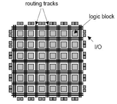
Figure 1: (a) Abstract FPGA architecture
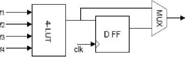
Figure 1: (b) logic block;
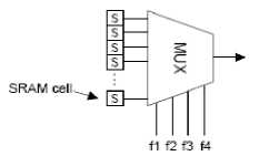
Figure 1: (c) LUT
Modern FPGAs consist of programmable logic resources embedded in a sea of programmable interconnects. The programmable logic resources can be configured to implement any logic function, while the interconnects provide the flexibility to connect any signal in the design to any logic resource. The programming technology for the logic and interconnect resources can be Static Random Access Memory (SRAM), flash memory [6], or antifuse [7, 8]. SRAM-based FPGAs offer incircuit reconfigurability at the expense of being volatile, while antifuse are write-once devices. Flash-based FPGAs provide an intermediate alternative by providing reconfigurability as well as non-volatility. The most popular programming technology in state-of-the-art FPGAs is SRAM.
Traditionally, FPGAs consist of input/output pads, logic resources, and routing resources. However, state-of-the-art FPGAs usually include embedded memory, DSP blocks, Phase-Locked Loops (PLLs), embedded processors, and other special feature blocks, as shown in Figure 2. These features allowed FPGAs to be an attractive alternative for some SoPC designs. The next Sections shed light on some of the available commercial FPGA architectures and FPGA CAD flow.
-
2.1 FPGA Logic Resources Architecture
-
2.1.1 Altera Stratix III Logic Resources
The logic blocks in FPGAs are responsible for implementing the functionality needed by each application. Increasing the functional capability of the logic blocks increases the number of
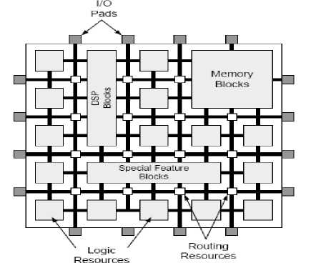
Figure 2.: Modern FPGA fabric logic functions that can be packed into it. Moreover, increasing the size of logic blocks, i.e., increasing the number of inputs to each logic block, increases the number of logic functions performed by each logic block as well as improving the area/delay performance of the logic block [9]. However, this comes on the expense of wasted resources because not all of the blocks will have all of their inputs fully utilized.
Most commercial FPGAs employ look-up tables (LUTs) to implement the logic blocks. A k-input LUT consists of 2k configuration bits in which the required truth table is programmed during the configuration stage. The almost standard number of inputs for LUTs is four, which was proven optimum for area and delay objectives [10]. However, this number can vary depending on the targeted application by the vendor. Moreover, modern FPGAs utilize a hierarchical architecture where every group of basic logic blocks is grouped together into a bigger logic structure, logic cluster. The remaining of this Section describes the programmable logic resources in two of the most popular commercial FPGAs.
The logic blocks in Altera's Stratix III are called Adaptive Logic Modules (ALMs). An 8-input ALM contains a variety of LUT-based resources that can be divided between two adaptive LUTs [11]. Being adaptive, ALMs can perform the conventional 4-input LUT operations as well as implementing any function of up to 6-inputs and some 7-input functions. Besides the adaptive LUTs, ALMs contain two programmable registers, two dedicated full adders, a carry chain, a shared arithmetic chain, and a register chain. Using these components, ALMs can efficiently perform arithmetic and shift operations. A detailed view of an ALM is shown in Figure 3. Every eight ALMs are grouped together to form a Logic Array Block (LAB).
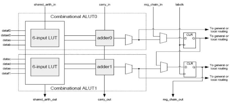
Figure 3: Altera's Stratix III ALM architecture
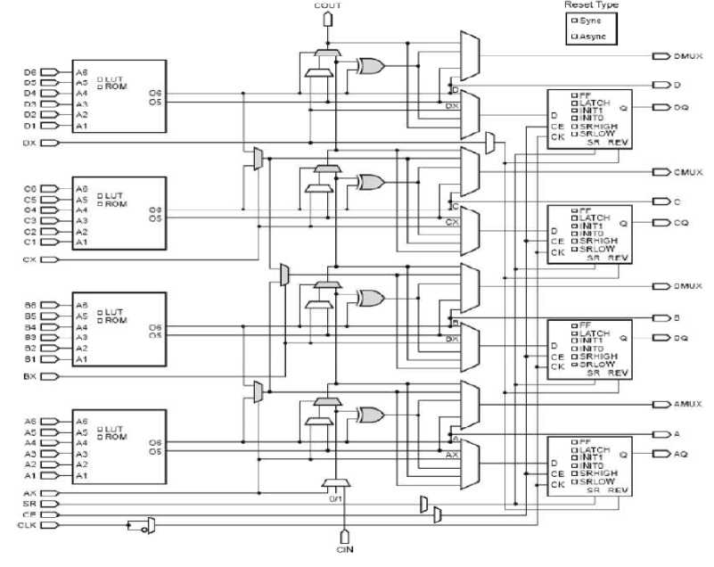
Figure 4: Xilinx's Vertex-5 slice architecture
-
2.1.2 Xilinx Virtex-5 Logic Resources
-
2.2 FPGA Routing Resources Architecture
-
2.3 CAD tools for FPGAs
The slice is the basic logic resource in Xilinx Virtex-5 FPGAs. Slices consist of four LUTs, wide function multiplexers, and carry logic [12]. Figure 4 shows the architecture of a typical Virtex-5 slice. The slices employ four 6-LUTs that are capable of performing any 6-input logic function. Functions with up to 8-inputs can be implemented using multiplexers to combine the output of two LUTs. Every two interconnected slices are grouped together in a Configurable Logic Block (CLB) [12].
Routing resources in FPGAs can be divided into two components; segmented local routing and dedicated routing. Segmented local routing is used to provide connection among the logic blocks. As depicted in Figure 5, the segmented wires are prefabricated in channels to provide programmable connections between switch blocks, connection blocks, and logic blocks. The number of wires in one channel is usually denoted by W [13].
The I/O of the logic blocks are dynamically connected to the segmented routing channels on all four sides using connection blocks. The number of wires in each channel to which a logic block pin can connect to is called the connection block flexibility Fc. In addition, the switch blocks provide programmable connectivity between the horizontal and vertical wires. The switch block flexibility Fs is defined as the number of wires to which each incoming wire can connect to in a switch block. The segment length of a certain wire segment is defined as the number of logic blocks spanned by the routing wire. Modern FPGAs use a combination of wires of different segment lengths to achieve the optimum performance in terms of routability, delay, or both.
Dedicated routing is used for global signals that fan out to a large number of logic blocks, e.g., clock and reset, thus providing low-skew. Moreover, some commercial FPGAs employ PLLs and Delay-Locked Loops (DLLs) for further skew reduction. Modern FPGAs have the flexibility to provide different clock domains inside the FPGA to enable asynchronous designs.
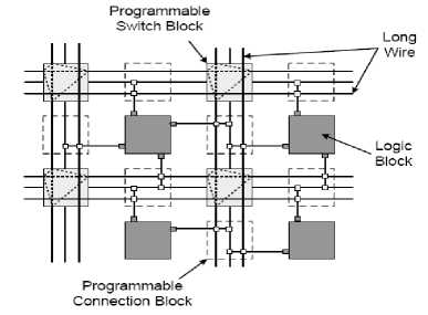
Figure 5: Routing resources in island-style FPGAs
FPGAs are implemented using a huge number of programmable switches that are used to implement a certain logic function. The CAD tools of FPGAs transform the design, entered either as a schematic or using a hardware description language, to a stream of `1's and `0's that program the FPGA during the configuration time. The flow chart in Figure 6 shows the different steps involved in the CAD flow for a typical FPGA design.
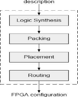
Figure 6: A typical FPGA CAD flow
-
a) Logic Synthesis
In the synthesis phase, the circuit description is converted to a netlist of basic logic gates. This phase is usually divided into two different stages; logic optimization and technology mapping [14-17]. Logic optimization is a technology-independent stage that involves simplifying the logic function of the design without the use of any technology information. Any redundant logic is removed at this stage. The optimized user circuit is then mapped into LUTs and flip-flops in the technology mapping stage, where each k-bounded logic function in the circuit is mapped into a k-LUT. This step resolves to find a set of k-feasible cuts that include all the nodes in the circuit in such a way to minimize the delay, area, and/or power dissipation of the final implementation. The process of technology mapping is often treated as a covering problem.
-
b) Packing
The packing phase converts the netlist of LUTs and flip-flops into a netlist of logic locks. The input netlist is converted into clusters of logic blocks that can be mapped into the physical logic blocks of the FPGA. Most packing algorithms minimize the number of resulting logic blocks, the number of connections between them, and/or the delay along the critical path. The packing algorithm has to consider the physical limitations of the actual logic blocks of the FPGA in terms of the maximum number of LUTs in a logic block and the number of distinct input signals and clocks a logic block has. Packing algorithms can be categorized as either bottom-up [14, 18, 19, and 20] or top-down [21, 22]. Bottom-up packing algorithms build each cluster individually around a seed LUT until the cluster is full. However, top-down packing approaches partition the
LUTs into clusters by successive circuit subdivision. Bottom-up algorithms are much faster and simpler than top-down approaches because they only consider local connections. However, this comes at the expense of solution quality.
-
c) Placement
In the placement phase, the packed logic blocks are distributed among the physical logic blocks in the FPGA fabric. Placement algorithms try to minimize the delay along the critical path and enhance the resulting circuit routability. Available placement algorithms can be classified into three categories; min-cut [23, 24], analytic [25, 26], and simulated annealing [27, 28, 29] based algorithms. Most of the commercial placement tools for FPGAs employ simulated annealing-based algorithms because of their flexibility to adapt to a wide variety of optimization goals. Simulated annealing (SA) placement tools depend on the SA algorithm, which is derived from the annealing process used to cool molten metals [30].
-
d) Timing Analysis
Timing analysis [31] is used to guide placement and routing CAD tools in FPGAs to: (1) determine the speed of the placed and routed circuit and (2) estimate the slack of each source-sink connection during routing to identify the critical paths. Timing analysis is usually performed on a directed graph representing the circuit, where the nodes represent LUTs or registers and the edges represent connections.
-
e) Routing
The routing phase assigns the available routing resources in the FPGA to the different connections between the logic blocks in the placed design [28]. The objective of a typical routing algorithm is to minimize the delay along the critical path and avoid congestions in the FPGA routing resources. Generally, routing algorithms can be classified into global routers and detailed routers. Global routers consider only the circuit architecture without paying attention to the number and type of wires available, while detailed routers assign the connections to specific wires in the FPGA.
-
III. POWER DISSIPATION IN FPGAS
First let us see what makes FPGAs to consume more power. As in all integrated circuits, FPGAs dissipate static and dynamic power. Static power is consumed due to transistor leakage and is dissipated when current leaks from the power supply to ground through transistors that are in the “off-state” due to sub-threshold leakage (from source to drain), gate-induced drain leakage, and gate direct-tunneling leakage. Dynamic power is consumed by toggling nodes as a function of voltage, frequency, and capacitance and is dissipated when capacitances are charged and discharged during the operation of the circuit.
FPGAs consume much more power than ASICs because they have a large number of transistors per logic function in order to program the device as explained above. Nevertheless, programmability is the essence of this technology and this overhead must be assumed. The extra circuitry that provides flexibility to an FPGA affects both the static and dynamic power dissipated by the FPGA. FPGA contains a large number of configuration bits, both within each logic element and in the programmable routing used to connect logic elements. Each of these configuration bits dissipates static power whereas an ASIC does not contain any such programming bits, and thus would consume significantly less static power than an FPGA. In addition, since the lookup-tables consume significantly more transistors than the corresponding logic in an ASIC, the static power dissipated in the logic is larger in an FPGA than in an ASIC.
In both an ASIC and FPGA, connections between gates are associated with some amount of parasitic capacitance due to the metal wire used to implement the connection as well as the driver and driven transistors. However, as described above, a connection in an FPGA also contains a large number of programmable switches. These switches significantly increase the parasitic capacitance on each wire segment and charging and discharging of this parasitic capacitance consumes more dynamic power. For all the reasons outlined above, an FPGA is significantly less power-efficient than an ASIC.
Tuan and Lai in [32] examined leakage in the Xilinx Spartan-3 FPGA, a 90nm commercial FPGA. Figure 7 shows the breakdown of leakage in a Spartan-3 CLB, which is similar to the Virtex-4 CLB. Leakage is dominated by that consumed in the interconnect, configuration SRAM cells, and to a lesser extent, LUTs. Combined, these structures account for 88% of total leakage.
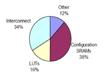
Figure 7: Leakage power breakdown in Xilinx Spartan-3
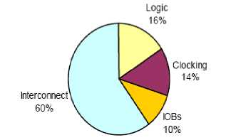
Figure 8: Dynamic power breakdown in XilinxVirtex-II
As pointed out in [32], the contents of an FPGA's configuration SRAM cells change only during the FPGA's configuration phase. Configuration is normally done once at power-up. Therefore, the speed performance of an FPGA's SRAM configuration cells is not critical, as it does not affect the operating speed of the circuit implemented in the FPGA. The SRAM cells can be slowed down and their leakage can be reduced or eliminated using previously-published low leakage memory techniques or by implementing the memory cells with high-VTH or long channel transistors. Leakage was not a primary consideration in the design of Spartan-3. If SRAM configuration leakage were reduced to zero, the Spartan-3 interconnect and LUTs would account for 55% and 26% of total leakage, respectively.
A number of recent papers have considered the breakdown of dynamic power consumption in FPGAs [33, 34, 35]. In [35] Shan studied the breakdown of power consumption in the Xilinx Virtex-II commercial FPGA. The results are summarized in Figure 8. Interconnect, logic, clocking, and the I/Os were found to account for 60%, 16%, 14%, and 10% of Virtex-II dynamic power, respectively. A similar breakdown was observed in [33]. The FPGA power breakdown differs from that of custom ASICs, in which the clock network is often a major source of power dissipation [36].
The dominance of interconnect in FPGA dynamic power is chiefly due to the composition of FPGA interconnect structures, which consist of pre-fabricated wire segments, with used and unused switches attached to each wire segment. Such attached switches are not present in custom ASICs, and they contribute to the capacitance that must be charged/ discharged in a logic transition. Furthermore, SRAM configuration cells and circuitry constitute a considerable fraction of an FPGA's total area. For example, [37] suggests that more than 40% of an FPGA's logic block area is SRAM configuration cells. Such area overhead makes wire lengths in FPGAs longer than wire lengths in ASICs. Interconnect thus presents a high capacitive load in FPGAs, making it the primary source of dynamic power dissipation.
-
IV. POWER REDUCTION TECHNIQUES
-
4.1 Leakage and Static Power Reduction
As stated above there are two primary types of power consumption in FPGAs: 1) Leakage and static power and 2) dynamic power. The techniques that are commonly used to reduce these two types of power consumptions have been explored in the following sub-sections:
Vendors such as Altera and Xilinx incorporate various low-power device-level technologies in their latest FPGA devices. Traditional FPGAs and ASICs only used two oxide thicknesses (dual oxide): a thin oxide for core transistors and a thick oxide for I/O transistors. Moving toward high-performance 90 nm FPGAs, Xilinx integrated circuit (IC) designers started to adopt the use of a third-gate oxide thickness (triple oxide) of midox in the transistors of the 90 nm Virtex™-4 FPGAs that allows a dramatic reduction in overall leakage, and hence static power, compared to other competitive FPGAs. Virtex-5 FPGAs continue to deploy the triple oxide technology in the 65 nm process node to enable a significant lower leakage current, about 38% lower than what the industry expects for a 65 nm device. At the device level, Altera and Xilinx both utilize triple gate oxide technology, which provides a choice of three different gate thicknesses, to trade-off between performance and static power [38][39]. In earlier technologies, only two thicknesses were available. Transistors with thicker oxide were used for the large, higher voltage tolerant transistors in the I/O blocks and the thinner ones were used everywhere else. The new medium thickness oxide transistors provide slightly less performance than thin oxide transistors, but leak significantly less power. These are used in the configuration memory and the switches that are controlled by this memory in the latest FPGAs. The oxide thickness does not affect the performance of the corresponding switches because the configuration memory remains static during the operation of the device.
Two recent papers focused on optimizing leakage in the unused portion of an FPGA. Calhoun proposed the creation of fine-grained “sleep regions", making it possible for a logic block's unused LUTs and flip-flops to be put to sleep independently [40]. A more coarse-grained sleep strategy was proposed in [41], which partitioned an FPGA into entire regions of logic blocks, such that each region can be put to sleep independently. The authors restricted the placement of the implemented design to fall within a minimal number of the pre-specified regions, and studied the effect of the placement restrictions on design performance.
One of few papers to address leakage in FPGA interconnect is [42], which applied well-known leakage reduction techniques to interconnect multiplexers. Four different techniques were studied. First, extra configuration SRAM cells were introduced to allow for multiple OFF transistors on unselected multiplexer paths. The intent is to take advantage of the “stack effect ", as illustrated in Figure 9(a). The left side of Figure 9(a) shows a typical routing switch multiplexer. Observe that there is a single OFF transistor on the unselected multiplexer path (highlighted). The right side of Figure 9(a) shows the redundant SRAM cell approach. The unselected path contains two OFF transistors, which limits sub threshold leakage along the path. A second approach described in [42] is to layout portion of the multiplexer in separate wells, allowing body-bias techniques to be used to raise the VTH of multiplexer transistors that are not part of the selected signal path [see Figure 9(b)]. Third, [42] proposes negatively biasing the gate terminals of OFF multiplexer transistors [Figure 9(c)]. The negative gate bias leads to a significant drop in sub threshold leakage. Finally, [42] proposes using dual-VTH techniques, wherein a subset of multiplexer transistors are assigned high-VTH (slow/low leakage), and the remainder of transistors are assigned low-VTH (fast/leaky). The dual-VTH idea, shown in Figure 9(d), impacts FPGA router complexity, as the router must assign delay-critical signals to low-VTH multiplexer paths. A more recent paper by Ciccarelli applies dual-VTH techniques to the routing switch buffers in addition to the multiplexers [43].
a) Redundant SRAM Cell
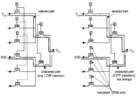
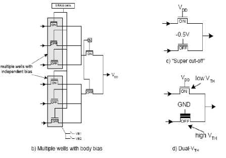
Figure 9: Multiplexer leakage reduction techniques
In the following sub sections some of technologies which have been used to reduce the leakage power in FPGA are discussed
-
4.1.1 Leakage Power Reduction in FPGAs Embedded Memories
-
4.1.2 Leakage Power Reduction Using Static Dual Threshold Techniques
-
4.1.3 Leakage Power Reduction Using Body-Biasing Techniques
Recently, FPGA vendors have started to increase the size of embedded memory cells in their FPGAs. It can be noticed that on average, high-performance FPGAs have a ratio of memory bits to logic cells of about 54, i.e., for every logic cell in the FPGA, there are 54 memory bits. On the other hand, for the low-cost FPGAs, the ratio drops to about 27. However, it can be noticed that the trend is toward increasing the ratio of memory bits to logic cells in low-cost FPGAs. It can be deduced that minimizing leakage power in the FPGA embedded memory is more beneficial than minimizing that of the logic cells. In [44] author proposed a CAD technique to reduce leakage power dissipation in FPGA embedded memory bits by adding path traversal and location assignment techniques in the embedded memory mapping. The authors assume that all the embedded memory cells can support the drowsy mode by having the ability to connect to two supply voltages VDDH and VDDL, a high and low supply voltage, respectively, as shown in Fig. 10. The flexibility to connect to either of the supply voltages is provided by two header PMOS devices that are controlled by two control signals. When the memory bit is operating at the low supply voltage, the bit will consume less leakage power, since leakage power is proportional to the supply voltage, while the cell still retains the stored data. This scheme for memory bits is referred to as drowsy memory.
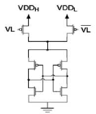
Figure 10. Drowsy Memory Architecture
Several techniques have been proposed in the literature to reduce leakage power in memories using the drowsy scheme; however, they mainly targeted cache memories in processors [45]. FPGA embedded memories have different characteristics when compared to cache memories. FPGA embedded memory accesses are statically scheduled and the data is stored statically, unlike cache memories that have variable latencies and dynamic data placement. Hence, the problem of minimizing leakage power in FPGA embedded memories helps in finding the best static layout of the data in the memory to maximize the leakage savings from putting the memories into a low-leakage state. The unused memory entries are placed in a sleep mode and are not to be brought out of that mode, while the used memory entries are put in a sleep mode when they are not accessed and waken up when needed.
In [44] author proposed three different modes: sleep mode, drowsy mode, and live mode. The sleep mode is used for unused memory entries by shutting down the supply voltage from the unused memory bits. In this case, the two PMOS header devices (in Fig. 10) are turned off and the data stored in the memory is lost. In the study the author showed that just by putting the unused memory entries in the sleep mode (used-active), one can save an average of 36% of the memory leakage power without utilizing any scheme for dynamically waking up(or putting to sleep) the used memory entries. Moreover, on average, about 75% of leakage power savings in the embedded memories can be achieved just by using the minimum number of memory entries and turning off the unused entries (min-entry). It is noticed that the drowsy-long scheme offers an additional 10% leakage power savings over the min-entry scheme. Moreover, the pathplace algorithm on an average achieves about 95% leakage power savings. Hence, it can be concluded that the two best memory layout techniques are the min-entry and path place techniques. The min-entry scheme offers very good leakage power savings in terms of both computational time and extra circuitry needed by the FPGA since it only supports active and off modes. On the other hand, the path-place scheme supports three memory modes: active, low leakage with data retention, and off modes.
Two architectures were proposed in [46] by the authors i.e. a homogeneous and a heterogeneous architectures, as shown in Fig. 11. The homogeneous architecture uses inside the cluster sub blocks of different VTH, while the heterogeneous architecture uses interleaved two types of clusters, where one of the clusters is composed of low VTH logic cells and the other consists of low and high VTH logic cells. The authors proposed a CAD framework that starts by assigning the whole design to high VTH logic cells. The algorithm then starts assigning the logic cells into low VTH cells as long as the cell has positive slack and the new path slack does not become negative. In the next stages, the algorithm clusters the logic cells into the clusters that correspond to the architecture being used. Finally, constrained placement is used to place the clustered designs into the FPGA architecture. It was noticed that both the homogeneous and heterogeneous architectures result in very close leakage power savings and delay penalties.
Body-biasing techniques are used to change the threshold voltage of the MOS devices. Increasing the body to source voltage (Vbs) of the MOS device from zero reduces the transistor delays on the expense of leakage power by reducing the device VTH [47]. Reducing Vbs to a negative value increases the device VTH and hence reduces the leakage current and increases the device delay. Figure 12 plots the relative in delay and power in a StratixTM FPGA that shows that a 20% increase in delay can result in about 2.5× reduction in leakage power. In the study, the authors proposed the use of body biasing in FPGAs to slow down the cells on non critical paths to achieve a reduction in the sub threshold leakage power. The authors concluded that using a granularity that is equal to two clusters results in considerably sufficient amount of leakage power savings without incurring big penalties on both the delay and area of the FPGA.
Low-V*TH
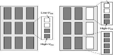
Homogeneous Heterogeneous
Figure 11 Dual Threshold Architectures
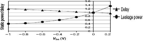
Figure 12 Power and delay vs. body bias
-
4.2 Dynamic Power Reduction
Dynamic power is consumed by toggling nodes as a function of voltage, frequency, and capacitance and is dissipated when capacitances are charged and discharged during the operation of the circuit and consumed during switching events in the core or I/O of FPGA. The dynamic power consumption is generally modeled as below:
P = L C i V i 2 . f.
i where C,V and f represent capacitance, the voltage swing, and clock frequency of the resource i, respectively [48]. The total dynamic power consumed by a device is the summation of the dynamic power of each resource. Because of programmability of FPGA the dynamic power is design-dependent and the factors that contribute to the dynamic power are: the effective capacitance of resources, the resources utilization, and the switching activity of resources [48], [49]. The effective capacitance corresponds to the sum of parasitic effects due to interconnection wires and transistors. Since FPGA architecture usually provides more resources than required to implement a particular design, some resources are not used after chip configuration and they do not consume the dynamic power (this is referred to as resource utilization). Switching activity represents the average number of signal transitions in a clock cycle. Though generally it depends on the clock itself, it may also depend on other factors (e.g. temporal patterns of input signals). Hence, the above equation can be rewritten as:
P = V2. f ^L Ci Ui. Si where V is the supply voltage, f is the clock frequency, and C , U , and S , are the effective capacitance, the utilization, and the switching activity of each resource, respectively [48].
The first comprehensive effort to develop a low-energy FPGA was by a group of researchers at UC Berkeley [50, 51, 52]. A power-optimized variant of the Xilinx XC4000 FPGA [X4K 02] was proposed. Power reductions were achieved through significant changes in the logic and routing fabrics. First, larger, 5-input LUTs were used rather than 4-LUTs, allowing more connections to be captured within LUTs instead of being routed through the power- dominant interconnect. Second, a new routing architecture was deployed, combining ideas from a 2dimensional mesh, nearest-neighbor interconnect, and an inverse clustering scheme. Third, specialized transmitter and receiver circuitry were incorporated into each logic block, allowing low-swing signaling to be used. Last, double-edge-triggered flip-flops were used in the logic blocks, allowing the clock frequency to be halved, and reducing clock power. The main limitations of the work are: 1) The proposed architecture represents a “point solution" in that the effect of the architectural changes on the area-efficiency, performance, and routability of real circuits was not considered; 2) The basis of the architecture is the Xilinx XC4000, which was introduced in the late 1980s and differs considerably from current FPGAs; 3) The focus was primarily on dynamic power and leakage was not a major consideration.
Power trade-offs at the architectural level were considered in [34], which examined the effect of routing architecture, LUT size, and cluster size (the number of LUTs in a logic block) on FPGA power-efficiency. Using the metric of power-delay product, [34] suggests that 4-input LUTs are the most power-efficient, and that logic blocks should contain twelve 4-LUTs. In these studies, despite their focus on power, power-aware CAD tools were not used in the architectural evaluation experiments, possibly affecting the architectural conclusions. Also, as in the UC Berkeley work [51], the architectures evaluated are somewhat out-of-step with current commercial FPGAs. For example, [34] suggests that a mix of buffered and unbuffered bidirectional routing switches should be used. Modern commercial FPGAs no longer use un-buffered routing switches; rather, they employ unidirectional buffered switches.
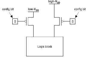
Dynamic power in CMOS circuits, computed through above equation depends quadratically on supply voltage. The quadratic dependence can be leveraged for power optimization, and this property has led to the development of dual or multi-VDD techniques, which have proved themselves effective at power reduction in the ASIC domain (e.g., [53, 54]). In a dual-VDD IC, circuitry that is not delay-critical is powered by the lower supply voltage; delay- critical circuitry is powered by the higher supply. Level converters are generally needed when circuitry operating at the low supply drives circuitry operating at the high supply. In [55], the dual-VDD concept is applied to FPGAs. A heterogeneous architecture is proposed in which some logic blocks are fixed to operate at high-VDD (high speed) and some are fixed to operate at low-VDD (low-power, but slower). Figure 13(a) illustrates one of the pre-defined dual-VDD fabrics studied in [55]. The power benefits of the heterogeneous fabric were found to be minimal, due chiefly to the rigidity of the fixed fabric and the performance penalty associated with mandatory use of low-VDD in certain cases. In [56], the same authors extended their dual-VDD FPGA work to allow logic blocks to operate at either high or low-VDD, as shown in Figure 13(b). Using such “configurable" dual-VDD schemes, power reductions of 9-14% (versus single-VDD FPGAs) were reported. A limitation of [56] and [56] is that the dual-VDD concepts were applied only to logic, not interconnect. The interconnect, where most power is consumed, was assumed to always operate at high-VDD. This limitation is overcome in [41A] which apply dual-VDD to both logic and interconnect.
A dual-VDD FPGA presents a more complex problem to FPGA CAD tools. CAD tools must select specific LUTs to operate at each supply voltage, and then assign these LUTs to logic blocks with the appropriate supply. To address these issues, algorithms for dual- VDD mapping and clustering have been developed in conjunction with the architecture work mentioned above [57, 58].
high-VCJ block----> □ □ □ □
low-VDD block
Pre-defined dual-VDD FPGA
b) Configurable dual-VDD logic block
Figure 13: Dual -VDD FPGA structures.
According to authors in [59], there are three major strategies in FPGA power consumption reduction. First, changes can be done at the system level (e.g. simplification of the algorithms used). Secondly, if the architecture of FPGA is already fixed, a designer may change the logic partitioning, mapping, placement and routing. Finally, if no changes at all are possible, enhancing operating conditions of the device may be still promising (this includes changes in the capacitance, the supply voltage, and the clock frequency).
The various techniques used for reducing dynamic power are broadly covered under following schemes:
-
• Reducing Dynamic Power on Clock Scheme
-
• Reducing Logic Power
-
• Reducing RAM Power
-
• Reducing I/O Power
-
4.2.1 Reducing Dynamic Power on Clock Scheme
The various techniques for dynamic power reduction under the above schemes are indicated in the following sections:
The following clock schemes are used to reduce dynamic power:
-
- Clock Gating at Chip Level that prevents the logic from switching in case of system-level clock gating and controls input and output states
and freezing clocks in case of using Flash *Freeze mode in Actel's flash-based FPGAs
-
- Clock Gating at Design Level or at RTL level is a commonly used power-saving technique with two types of clock gating: latch-based and latch-free clock gating. It is a straightforward substitution for RTL code. FPGA synthesis tools do not perform clock gating automatically. In this groups of flip-flops are identified that share a common enable term to implement combinational clock gating. Therefore, if a bank of flip-flops which share a common enable term use RTL clock gating. The flip-flops consume zero dynamic power as long as this enable term is false. However, one must be careful when implementing it because the skew between clock and enable signal could cause extra glitches.
-
- Global Resource Power Reduction by reducing the key elements i.e. frequency, the number of clock spines, the fan-out and loading on the global networks.
-
4.2.2 Reducing Logic Power
Careful selection of appropriate arithmetic blocks is a source of large power savings in computation oriented designs. This section goes over the power consumption of various arithmetic blocks and provides recommendations for reducing logic power.
ADDER AND MULTIPLIER
The synthesis tool library offers a wide variety of arithmetic blocks with several architectures to better fit the area and performance needs of designs. The following architectures are used for multiplier implementation: Carry-Save-Adders multiplier (CSA), Charge State Multiplier (CSM), Wallace and Non Booth Encoding Wallace (NBW) architectures. For adder, the architectures are the Forward Carry Look Ahead (CLF), the Brent and Kung (BK), the Carry Look-Ahead (CLA), the CSM, and the Ripple (RPL) adders. These are also available through various online resources. In general, the power numbers in the arithmetic blocks are dominated by routing and correlate to a wide spread of the wire lengths.
COUNTERS
Counters are commonly used throughout designs for many different functions, such as keeping track of elapsed time, loading RAM address or data busses, controlling a state machine's next state, or output logic. The power profiles for gray, binary, and ring counters reveal that the binary counters offer the lowest power, followed by the gray, while the composition of ring counters has the worst power figure, mainly because of the large load on the clock.
Finite State Machine (FSM) and Counter Encoding
The selection of the state assignment depends on several parameters, such as the complexity of the state machine (the number of states), the number of paths and their lengths, the number of fork situations, and the complexity of the predicates on transitions between states. One should control the encoding scheme for low-power design. The most effective way is to write the RTL directly into the intended encoding as opposed to letting synthesis decide the state encoding, because one can explicitly select encoding to minimize the number of bit changes per transition.
General Glitch Reduction Techniques on Logic
Glitches are unwanted switching activities that occur before a signal settles to its intended value. On every active clock edge, glitches can occur within combinatorial logic. This is because every node has a different delay, which means combinatorial logic may change states several times before settling down. Glitches on a node are dependent on the logic depth to that node—the number of logic gates from the node to the primary inputs (or sequential elements). The deeper and wider the logic cone behind a node, the more it will glitch. Unstable logic expressions, unbalanced sets of paths driving a sensitive combinatorial cell, or a MUX select line that can toggle several times within a clock period are examples of sources of glitches. Some of the glitches are absorbed by the cell delays and do not propagate. Some others, however, do propagate and can affect the power dissipation. Some general glitch reduction techniques used are by:
-
• Rearranging the logic
-
• Partitioning and Using Different Optimization Level
-
• Pipelining
-
• Inserting AND Gate on the Net Driver
-
• Logic Depth Reduction for Frequently Switching Signals
-
4.2.3 Reducing RAM Power
Analyzing power consumption during various operations brings to light several techniques for lowering the power contribution of the RAM blocks
-
• The write operation consumes slightly less power than the read access, so changing the RAM operation could reduce power consumption and reduce peak power.
-
• The study shows that the larger the Hamming distance between successive addresses, the larger the power consumption. So, it is recommended to reduce the Hamming distances between successive addresses in order to minimize the RAM power waste.
-
• When the same clock edge is used for the read and write, peak power consumption can be high due to simultaneous accesses on dual-port or two-port RAMs. It is therefore recommended to use clocks with opposite edges for these ports.
-
4.2.4 Reducing I/O Power
The I/O power consumption is similar to logic power because it depends on switching, load capacitance, frequency, and voltage. By reducing any one of these components, one can reduce the I/O power. Here are some guidelines for reducing I/O power:
-
• Choose low VCCI for I/O. Changing VCCI from 3.3 V to 1.5 V can save up to 80% of your I/O power.
-
• Reduce capacitive load to reduce the I/O power consumption.
-
• Use differential I/O standards and resistively-terminated I/O standards for highest toggling frequencies and single-ended I/O standards for low frequencies. The differential I/Os have higher static power, but have the lowest dynamic power because of the limited voltage swing. Having a choice as to which I/O standard to use, evaluate the options based on the anticipated activity of the I/Os.
-
• Reduce the number of I/Os by eliminating I/Os that can be time multiplexed.
-
• Use bus encoding that helps reduce the number of toggling bits and correlates successive values on the bus.
-
• Divide the active outputs into two groups, some at the positive edge of the clock and others at the opposite edge.
-
V. OVERVIEW OF POWER REDUCTION DESIGN TECHNIQUES
The various techniques which have been used for power reduction in FPGAs are broadly covered at the following three design levels:
-
a) System-Level
-
b) Device-Level
-
c) Architecture- and Circuit- Level
-
5.1 Power Reduction at System Level Design:
Looking at research works carried out to minimize power reduction techniques at system level design can be categorized in the following three parts:
-
• Basic techniques: Following basic techniques have been explored so far at system level design: - Preferably use coarse-grained embedded blocks rather than the fine-grained configurable logic blocks in an FPGA, since the former are more power efficient than the latter for the same function [60]. While using course-grained, it is to be ensured that power consumption for routing would not increase significantly.
-
- To obtain the best trade-off in speed, area, power consumption, flexibility, and accuracy, word-length optimization can be
applied. For adaptive filters and polynomial evaluations, improvements in power consumption of up to 98% (mean 87%) have been achieved [61].
-
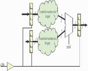
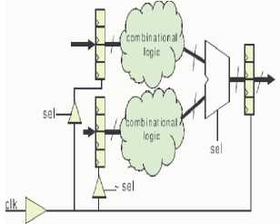
- Clock gating is a simple and effective method for reducing dynamic power consumption. It decreases dynamic power by eliminating unnecessary toggling on the outputs of flip-flops of a circuit, gates in the fan-out of the flip-flops, and clock signals. Fig. 14 depicts a classic example of clock gating. In part (a) of the figure, we see two register files on the left, each feeding a combinational logic circuit. The outputs of the two combinational logic circuits feed the inputs of a multiplexer. The multiplexer’s select signal, sel, selects which combinational circuit’s output is passed to the input of a destination register file. Part (b) of the figure shows the circuit after clock gating has been applied. The signal sel is used to derive a clock enable signal on clocks feeding the input register files. Power is reduced through several mechanisms. First, the capacitive loading on the clock network itself is reduced. Second, unnecessary toggling within the combinational circuits is eliminated. In particular, in the optimized circuit, toggling only occurs in the combinational circuit whose output is selected by the multiplexer to be passed to the destination register file. Clock gating has been used extensively in ASICs for power optimization. However, clock gating has not been explored in depth for FPGAs as well and is different from ASICs because of the fixed pre-fabricated clock interconnection network. It can be used to reduce dynamic power consumption to prevent signal transitions by disabling the clock for the inactive regions. The circuitry in an operator is gated when not in use if it can be combined with word-length optimization [62].
-
- It is found that, at a given clock speed, pipelining which is a simple and effective way of reducing glitching can reduce the amount of energy per operation by between 40% and 90% for applications such as integer multiplication, CORDIC, triple DES, and FIR filters [63].
-
- By using dynamic voltage scaling to adapt the dynamic supply voltage to the FPGA as the temperature changes, to minimize power consumption. Power reduction between 4% and 54% can be achieved for various arithmetic circuits [64].
Techniques with run-time reconfigurability
-
- Runtime reconfiguration with word-length optimization can be combined to adopt the
smallest design at a given time, as long as the energy reduction in execution is greater than the energy overhead for reconfiguration [62] .
- In order to adapt to run-time conditions, runtime reconfiguration can be applied to change a design. A more powerful but less energy efficient turbo coder can be used to maintain a fixed bit error rate, and vice versa when a communication channel becomes more noisy [65].
-
• Low-power techniques for FPGA-based soft processors
-
- Instruction set extensions based on an iterative improvement method to the Micro Blaze soft processor have been proposed in [66] wherein up to 40% reduction in energy and 12% reduction in peak power has been reported
-
- Combined application of instruction recoding and power-aware scheduling techniques can be used to optimize a soft processor at multiple levels of abstraction. Dynamic power reduction of up to 74% has been reported in [67].
-
5.2 Power Reduction at Device Level Design:
a) Before Gating
b) After Gating
Figure 14: Clock Gating-An Example
Vendors such as Altera and Xilinx incorporate various low-power device-level technologies in their latest FPGA devices. Traditional FPGAs and ASICs only used two oxide thicknesses (dual oxide): a thin oxide for core transistors and a thick oxide for I/O transistors. Moving toward high-performance 90 nm FPGAs, Xilinx integrated circuit (IC) designers started to adopt the use of a third-gate oxide thickness (triple oxide) of midox in the transistors of the 90 nm Virtex™-4 FPGAs that allows a dramatic reduction in overall leakage, and hence static power, compared to other competitive FPGAs. The new medium thickness oxide transistors provide slightly less performance than thin oxide transistors, but leak significantly less power. These are used in the configuration memory and the switches that are controlled by this memory in the latest FPGAs. The oxide thickness does not affect the performance of the corresponding switches because the configuration memory remains static during the operation of the device,
FPGA vendors in addition to smaller device geometries that reduce the average node capacitance, use a low-k dielectric between metal layers which reduce the parasitic capacitance and hence reduces the correspondingly dynamic power. Since the dynamic power has a quadratic relationship ( CV2f ) with the supply voltage, it can be reduced further by lowering the supply voltage. Xilinx reduces the core supply voltage from 1.2V being used in Virtex 4 to 1.0V in its Virtex 5 FPGAs that cuts core power significantly. Altera and Xilinx have also made a number of architecture-level changes to their latest devices to reduce static and dynamic power like both have recently increased the size of the LUTs (lookup tables) within the logic blocks. Since LUTs are implemented using smaller transistors (compared to transistors in the routing resources), which leak less and dissipate less dynamic power therefore, both static and dynamic power are reduced by increasing the size of the basic logic elements, from 4-input LUTs to 6 and 7-input LUTs, since more logic is implemented within each LUT and less routing is needed between the LUTs. Other features at architecture-level that reduce overall power are use of the embedded memories, adders, and multipliers. Although each of these functions can be implemented using the programmable logic fabric, its implementation as a fixed-function embedded block is more power-efficient since circuitry to make it flexible is not needed, and it can be turned off when not used. Moreover, vendors have also modified their routing architectures that reduce the average capacitance of the routes, which improves both power and performance.
A number of low-power techniques have also been incorporated into the commercial FPGA CAD tools. Detailed power models have been integrated within the Altera Quartus II [68] and Xilinx ISE CAD tools [69] that provide a spreadsheet utility to make early power predictions before the design is complete and a detailed power model that can be used when the design is complete. The detailed power models provide estimates after the application has been placed, routed, and simulated whereas early power estimates are based on estimated resource usage, I/O types, clock requirements, clock frequencies, and environmental conditions. The estimations from the detailed power models are more accurate than those from the early power models, since detailed capacitance, leakage, and switching activity information is known for each node in the application circuit. Power-aware CAD techniques have also been incorporated into the commercial CAD flows. Power is minimized during technology mapping, placement and routing by minimizing the capacitance of high-activity signals in Quartus II. As described in [70], power is also minimized by optimizing the mapping to the embedded memories and to the embedded DSP blocks. In ISE, power is minimized during placement and routing by minimizing the capacitance of high-activity signals. Dynamic power dissipation is further minimized by strategically setting the configuration bits within partially used (some inputs are not used) LUTs to minimize switching activity. Altera reports that Stratix III FPGAs are over 50% more power efficient than Stratix II FPGAs [68] by combining the above techniques and similarly, Xilinx reports that Virtex-5 FPGAs consume over 35% less dynamic power than Virtex-4 FPGAs, with even greater savings when embedded components are used [39]. Xilinx also points out that low leakage techniques are already incorporated in their Virtex-4 FPGAs, resulting in 70% lower static power consumption when compared with competing FPGAs.
A low-power alternative to SRAM-based FPGAs is flash-based FPGA technology as flash-based memory dissipates significantly less leakage power compared to SRAM memory. Actel’s devices which are Flash-based FPGAs, are inherently more efficient and it is reported that their low-power FPGAs dissipate 4 times less leakage power than their nearest competitors [71].
-
5.3 Power Reduction at Architecture- and CircuitLevel Design:
A number of studies have investigated low-power FPGA architecture design. The authors in [72][73] have described energy-efficient FPGA routing architectures and low-swing signaling techniques to reduce power, whereas, a new FPGA routing architecture that utilizes a mixture of hardwired and traditional programmable switches is proposed In [74], which reduces static and dynamic power by reducing the number of configurable routing elements. The architecture and the circuit-level implementation of the FPGA is key in reducing power, since it directly affects the efficiency of mapping applications to FPGA resources, and the amount of circuitry to implement these resources. In [75], the author introduced the energyefficient modules for embedded components in FPGAs to reduce power by optimizing the number of connections between the module and the routing resources, and by using reduced supply voltage circuit techniques. A novel FPGA routing switch with high-speed, low-power, or sleep modes have been presented in [76]. The switch reduces dynamic power for non timing critical logic and standby power for logic when it is not being used. The author reported lower energy up to 3.6 times than an ARM7 device, and up to 6 times lower energy than a C55X DSP, by using several power reduction techniques, such as register file elimination and efficient instruction fetch that are proposed for a coarse-grain reconfigurable cell-based architecture in [77]. Power-gating is applied to the switches in the routing resources to reduce static power and duplicate routing resources, that use either high or low Vdd, are used to reduce dynamic power in [78]. The rest of this section describes two recent improvements: minimization of FPGA glitch power, and efficient FPGA clock network design.
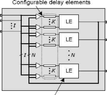
Dynamic power is a result of signal transitions between logic-0 and logic-1. These transitions can be split into two types: functional transitions and glitches. Functional transitions are those which are necessary for the correct operation of the circuit. Glitches, on the other hand, are transitions that arise from unbalanced delays to the inputs of a logic gate, causing the gate’s output to transition briefly to an intermediate state. Although glitches do not adversely affect the functionality of a synchronous circuit (as they settle before the next clock edge), they have a significant effect on power consumption. A recent study in [79] suggests that glitching accounts for 31% of dynamic power dissipation in FPGAs. Glitching occurs when values at the inputs of a LUT toggle at different times due to uneven propagation delays of those signals. If the arrival times are far enough apart, spurious transitions can be produced at the LUT output, as shown in Figure 15(a). Detailed timing information is used to configure these delay elements after place and route, so as to align the arrival times at the inputs of each logic element and this eliminates glitches as long as the arrival times can be aligned closely enough, as shown in Figure 15(b).The study in [79] proposes a method for minimizing glitching which involves adding configurable delay elements to the inputs to each logic element in the FPGA (Figure 16). The amount of elimination of glitching depends on several factors like resolution, maximum delay, location and amount of the programmable delay elements. On an average, the proposed technique eliminates 87% of the glitching that reduces overall FPGA power by 17% at the cost of the overall FPGA area by 6% and critical-path delay by less than 1% due to the added circuitry increases. The method can further be applied to all commercial FPGAs, and requires only minor changes to the CAD flow or the rest of the architecture.
Glitch reduction techniques can be applied at various stages in the CAD flow. Since glitches are caused by unbalanced path delays to LUT inputs, it is natural to design algorithms that attempt to balance the delays. This can be done at the technology mapping stage [80], in which the mapping is chosen based on glitch-aware switching activities. Another approach operates at the routing stage [81], in which the faster arriving inputs to a LUT are delayed by extending their path through the routing network. Delay balancing can also be done at the architectural level. However, these approaches all incur an area or performance cost. Some works use flip-flop insertion or pipelining to break up deep combinational logic path which are the root of high glitch power. Circuits with higher degrees of pipelining tend to have lower glitch power because they have fewer logic levels, thus reducing the opportunity for delay imbalance [82]. Flip flops with shifted-phase clocks can be inserted to block the propagation of glitches [83]. Another work in [84] uses negative edge-triggered flip-flops in a similar fashion, but without the extra cost of generating additional clock signals. It is also possible to apply retiming to the circuit by moving flip-flops to block glitches [85].
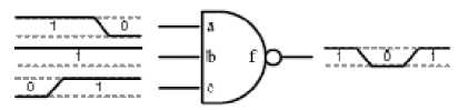
Figure 15(a) Circuit with glitch
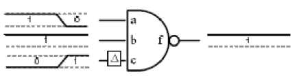
Figure 15(b) Glitch removed by delay input C
The authors in their paper present a glitch reduction optimization algorithm based on don’t-cares that sets the output values for the don’t-cares of logic functions in such a way that reduces the amount of glitching [86]. This process is performed after placement and routing, using timing simulation data to guide the algorithm.
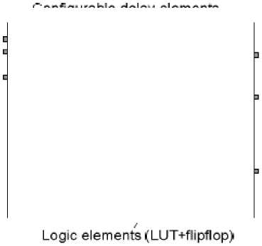
Figure 16 FPGA logic Block with configurable Delay elements
The algorithm achieved an average total dynamic power reduction of 4.0%, with a peak reduction of 12.5%; glitch power was reduced by up to 49.0%, and 13.7% on average. Future work will involve integrating the algorithm into a fully power-aware FPGA CAD flow, and investigating whether other stages of the CAD flow could improve its effectiveness. This approach leverages the ability to re-program FPGA logic functions without altering the placement and routing. Since the placement and routing are maintained, this optimization has zero cost in terms of area and delay, and can be executed after timing closure is completed
Another recent improvement is related to low-power clock network design. The basic element for implementing combinational logic in Virtex-5 is called a configurable logic block (CLB) that contains two SLICEs, each of which contain four 6-input look-up-tables (LUTs) and four registers. A Virtex-5 SLICE and CLB are shown in Figure 17. Each CLB’s inputs and outputs connect to a programmable interconnection network that permits CLBs to be connected to one another, as needed for the design implemented in the FPGA. In addition to CLBs, the Virtex-5 fabric contains large hard-IP blocks, such as block RAMs and DSPs, as well as tiles for I/O, clock management and varied other tiles. The Virtex-5 FPGA is designed to accommodate many different clock signals. Global clock buffers (BUFGs) within Virtex-5 receive clock signals, from either external or internal sources, and feed such signals into the dedicated global clock interconnection network. The global clock interconnection network distributes clock signals throughout the FPGA with low- skew, low-jitter and low-power. Each Virtex-5 chip contains 32 global clock buffers and therefore, can support the presence of 32 global clock signals in the design. Instead, the Virtex-5 fabric is partitioned into clock regions for the purposes of clock distribution. Clock regions in Virtex-5 are 20 CLBs tall and span half of the Virtex-5 die horizontally. Up to 10 global clock signals may be fed into any given region. The 10 global clocks within a region may be selected from any of the 32 global clock signals present in the design. Figure 18 indicates the eight regions in the Virtex-5 LX30 FPGA; larger members of the Virtex-5 family will contain more regions. It can be observed that up to 10 clock signals, driven by 32 BUFGs, are selected to be driven into the clock region.
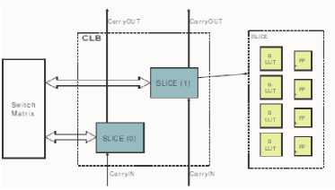
Figure 17 Virtex 5 FPGA
Global Clock Buffers
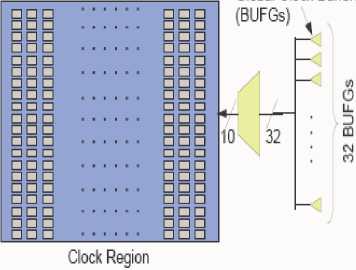
Figure 18 Clock Region in Virtex 5
Clock gating involves selectively disabling the clock signal from reaching sequential elements in the design. Here, we introduce two clock enable mechanisms built-in to Virtex-5 that may be used for realizing clock gating. Figure 19(a) shows that the registers within a SLICE have a clock enable pin, permitting clock enables to be implemented at a fine level of granularity. All registers in the SLICE must receive the same clock enable signal. Figure 19(b) depicts that the global clock buffer (BUFG) that drives clock signals into the dedicated clock interconnection network has an enable pin.
Figure 20 shows a detailed view of the interconnect structure within a clock region. There are 10 root spines (shown as dark lines in the figure) horizontally crossing the center of the region 2 At the intersection of each column, each horizontal root spine can be programmably connected to two vertical spines: one traveling north for the top-half of the region, and one traveling south for the bottom-half of the region. The vertical spines are shown as vertical dashed lines in Figure 20. Since there are 10 horizontal root spines in a region, there are 20 vertical spines for each column of the region. The logic blocks in the region receive their clock signals from the vertical spines. Each upper or lower vertical spine corresponds to a single horizontal root spine. Every horizontal root spine can be driven by one of 32 global clock buffers (BUFGs)
The power consumption of a clock signal within a clock region is mainly determined by the number of vertical spines connected to the root spine. A root spine is only connected to a vertical clock spine if the placement necessitates it. If a horizontal root spine carries a clock signal, clkA, connections to a vertical spine will only happen for those half-columns containing a load of clkA. Vertical clock spines contribute significantly to the capacitance of the clock signal, thereby affecting clock power. Indeed, the total power consumption for a clock signal is strongly tied to the sum of the number of vertical spines used in all the clock regions within which the load components of the clock are placed. Roughly 90% of clock network capacitance is contributed by vertical spines in typical designs.
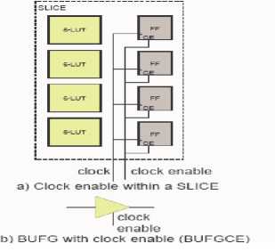
Figure 19 Clock Enable Options
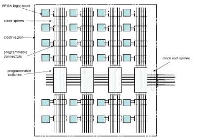
Figure 20 Clock Region Interconnect Detail
For clock-aware FPGA placement, the only works to consider CAD and architecture for reducing FPGA clock net work power are those of Lamoureux and Wilton [87, 88], and the very recent paper by Vorwerk et al. at Actel [88]. Modern FPGAs are partitioned into regions, with limitations on the number of clock signals that may be routed into any given region. The placer in [89] minimizes the number of regions spanned by a clock network and also minimizes the number of resources used within regions, thereby reducing clock routing capacitance.
In [90], clock network power in field-programmable gate arrays (FPGAs) is considered and two complementary approaches for clock power reduction in the Xilinx RVirtexTM-5 FPGA are presented. In this paper, the authors do not consider which clocks should be routed on global versus regional clock resources and the placer assumes such decisions have already been made. However, like [87], the placer does consider minimizing the clock network resources used within a region, albeit using what can be viewed as an extension of the placement algorithm in [87]. The approaches are unique in that they leverage specific architectural aspects of Virtex-5 to achieve reductions in dynamic power consumed by the clock network. The first approach comprises a placement-based technique to reduce interconnect resource usage on the clock network, thereby reducing capacitance and power (up to 12%). The second approach borrows the “clock gating” notion from the ASIC domain and applies it to FPGAs. Clock enable signals on flip-flops are selectively migrated to use the dedicated clock enable available on the FPGA’s built-in clock network, leading to reduced toggling on the clock interconnect and lower power (up to 28%). Power reductions are achieved without any performance penalty, on average.
It is observed from the literature that the dynamic power consumption is supposed to increase linearly with changes of clock frequency and size of a design. It was observed that with the clock frequency decrease the effect of the design size on power consumption gets decreased [90]. For example, for 2MHz clock frequency the total dynamic power consumption for designs with 3 and 24 copies of EWMA filter is equal to 26mW and 40mW, respectively. However, for the clock frequency of 20MHz, the total dynamic power consumption for the same designs is equal to 63mW and 238mW, respectively. FPGA designs can be enlarged with a disproportionally low dynamic power increase as long as the device operates at low frequencies. Only at the highest frequencies, the dynamic power changes proportionally to the design area.
The usage of multiple clock domains is a well known technique that allows performance increase, and power and/or energy decrease. This is only discussed at low level of designing process earlier. The concept of multiple clock domains was implemented at a high-level of designing process, the dynamic power is more important from the designer’s perspective as it can be controlled/reduced even at the system level by applying proper design methodologies [91].
Although designs occupying a large portion of FPGA resources, map, place and route tools try to achieve desired performances by spreading the logic of each particular clock domain over a wider area of the chip, but this may increase the power consumption since additional routing resources must be used to interconnect relevant logic. However, as seen in [91], even for large designs that utilize 41% and 59% of available slices, a significant power consumption reduction is still possible. The obvious fact that lower clock frequencies reduce dynamic power can be supplemented with some additional observations. First, point to notice was that when the clock frequency decreases, the size of a design becomes almost unimportant (from the perspective of dynamic power consumption).
It is further recommended to conveniently maintain the same performance of a particular design by reducing its clock frequency and by introducing the increased level of parallelism that allow more operations executed simultaneously within one clock cycle while maintaining the same energy per operation. Though the hardware resources are significantly increased (due to additional hardware resources required by the parallelism introduced), the dynamic power consumption increase can be negligible (if a sufficiently low clock frequency is applied). Although generally small FPGA chips should be used for small designs, the advantages of large FPGAs should not be ignored.
Following three parts described in the research works in [87] [88] examine the trade-off between the flexibility of FPGA clock networks and overall power consumption.
-
- A parameterized framework for describing a wide range of FPGA clock networks.
-
- A comparison of clock aware placement techniques to determine their effectiveness: since clock networks impose hard constraints on the placement of logic blocks within the FPGA, a good clock-aware placement algorithm must obey these constraints and also optimize for speed, routability, and power consumption.
-
- Several techniques for combining these objectives are evaluated, in terms of their ability to find a placement that is fast, energy efficient, and legal.
-
VI. CONCLUSION
Trends in technology scaling imply a drastic increase in leakage power and a steady increase in dynamic power with each successive process generation. Field-programmable gate arrays (FPGAs) require considerable hardware overhead to offer programmability, making them less power-efficient than custom ASICs for implementing a given logic circuit. The huge numbers of transistors on the largest FPGA chips suggest that the power trends associated with scaling may impact FPGAs more severely than custom ASICs. Despite this, until recently, the majority of published research on FPGA CAD and architecture, as well as the focus of the commercial vendors, has been on improving FPGA speed and density. Power management in FPGAs will be mandatory to ensure correct functionality, provide high reliability, and to reduce packaging costs. Furthermore, lower power is needed if FPGAs are to be a viable alternative to ASICs in low-power applications, such as battery-powered electronics.
This paper summarizes the different works that have been carried out and various techniques used at system, device, and architecture and circuit level to reduce the power consumption of FPGAs. It describes many of the significant improvements which have been made to improve power and energy efficiency of FPGAs that ranges from low level processes and circuit design techniques to high level techniques. Although significant improvements have already been made, many opportunities to further reduce power in FPGAs remain. Three areas that we feel are particularly fertile are glitch, low-power clock network design and leakage optimization. FPGAs with embedded processors and soft-processors are already available. This introduces similar system-level tradeoffs and the potential for significant power savings. Research targeting low-power system-level benchmarks is also required. While further improvements will likely be made at all levels, there seems to be significant potential for power savings at the system level. At the system level, power reduction can be obtained by optimizing management and scheduling of system resources.
Continued advances in low power software and hardware will open the door for FPGAs entering new powersensitive markets
References Reduction of Power Consumption in FPGAs - An Overview
- I. Kuon and J. Rose, "Measuring the Gap Between FPGAs and ASICs," ACM/SIGDA International Symposium on Field-Programmable Gate Arrays, pp. 21-30, 2006.
- V. Betz., J. Rose, and A. Marquardt, "Architecture and CAD for deep-submicron FPGAs," Kluwer Academic Publishers, 1999.
- J. Cong and S. Xu, Technology mapping for FPGAs with embedded memory blocks, in ACM/SIGDA International Symposium on Field-Programmable Gate Arrays (FPGA), pp.179-188, 1998
- S. J. E. Wilton, "SMAP: heterogeneous technology mapping for area reduction in FPGAs with embedded memory arrays," in ACM/SIGDA International Symposium on Field-Programmable Gate Arrays (FPGA), pp. 171-178, 1998.
- International Technology Roadmap for Semiconductors, "International technology roadmap for semiconductors 2005," 2005.
- K. J. Han, N. Chan, S. Kim, B. Leung, V. Hecht, B. Cronquist, D. Shum, A. Tilke, L. Pescini, M. Stiftinger, and R. Kakoschke, "Flash-based Field Programmable Gate Array Technology With Deep Trench Isolation," in Proc. of IEEE Custom Integrated Circuits Conf., 2007, pp. 89-91.
- S. D. Brown, "An Overview of Technology, Architecture and CAD Tools for Programmable Logic Devices," in Proc. of IEEE Custom Integrated Circuits Conf., 1994, pp. 69-76.
- J. Greene, E. Hamdy, and S. Beal, "Antifuse Field Programmable Gate Arrays," Proc. IEEE, vol. 81, no. 7, pp. 1042-1056, July 1993.
- E. Ahmed and J. Rose, "The Effect of LUT and Cluster Size on Deep Submicron FPGA Performance and Density," in Proc. of ACM Intl. Symp. on Field Programmable Gate Arrays, 2000, pp. 3-12.
- J. Rose, R. J. Francis, D. Lewis, and P. Chow, "Architecture of Field-Programmable Gate Arrays: The Effect of Logic Block Functionality on Area Efficiency," IEEE J. Solid-State Circuits, vol. 25, no. 5, pp. 1217-1225, Oct.1990.
- Altera Corp. Stratix III Device Handbook. [Online]. Available: http://www.altera.com/literature/hb/stx3/stratix3 handbook.pdf
- Xilinx Inc. Vertix-5 FPGA User Guide. [Online]. Available: http://www.xilinx.com/support/documentation/user guides/ug190.pdf
- J. Rose and S. Brown, "Flexibility of Interconnection Structures for Field- Programmable Gate Arrays," IEEE J. Solid-State Circuits, vol. 26, no. 3, pp. 277-282, 1991.
- J. Cong and M. Smith, "A Parallel Bottom-Up Clustering Algorithm with Applications to Circuit Partitioning in VLSI Design," in Proc. of IEEE/ACM Design Automation Conf., 1993, pp. 755-760.
- J. Cong, J. Peck, and Y. Ding, "Rasp: A general logic synthesis system for SRAM-based FPGAs," in Proc. of IEEE/ACM Design Automation Conf., 1996, pp. 137-143.
- J. Cong, C. Wu, and Y. Ding, "Cut ranking and pruning: Enabling a general and efficient FPGA mapping solution," in Proc. of ACM Intl. Symp. on Field Programmable Gate Arrays, 1999, pp. 29-35.
- A. Ling, D. P. Singh, and S. D. Brown, "FPGA technology mapping: A study of optimality," in Proc. of IEEE/ACM Design Automation Conf., 2005, pp. 427-432.
- A. Marquardt, V. Betz, and J. Rose, "Using Cluster-Based Logic Blocks and Timing-Driven Packing to Improve FPGA Speed and Density," in Proc. Of ACM Intl. Symp. on Field Programmable Gate Arrays, 1999, pp. 37-46.
- J. Cong, L. Hargen, and A. B. Kahng, "Random Walks for Circuit Clustering," in Proc. of IEEE Intl. Conf. on Application Specific Integrated Circuits, 1991, pp. 14-21.
- J. Cong and S. K. Lim, "Edge Separability Based Circuit Clustering with Application to Circuit Partitioning," in Proc. of IEEE/ACM Asia South Pacific Design Automation Conf., 2000, pp. 429-434.
- L. W. Hagen and A. B. Kahng, "Combining Problem Reduction and Adaptive Multi-Start: a New Technique for Superior Iterative Partitioning," IEEE Trans. Computer-Aided Design, vol. 16, no. 7, pp. 709-717, July 1997.
- D. J.-H. Huang and A. B. Kahng, "When Clusters Meet Partitions: New Density-Based Methods for Circuit Decomposition," in Proc. of European Design and Test Conf., 1995, pp. 60-64.
- A. E. Dunlop and B. W. Kernighan, "A Procedure for Placement of Standard Cell VLSI Circuits," IEEE Trans. Computer-Aided Design, vol. 4, no. 1, pp. 92-98, 1985.
- D. J.-H. Huang and A. B. Kahng, "Partitioning-Based Standard-Cell Global Placement with an Exact Objective," in Proc. of ACM Intl. Symp. on Physical Design, 1997, pp. 18-25.
- J. M. Kleinhans, G. Sigl, F. M. Johannes, and K. J. Antreich, "GORDIAN: VLSI Placement by Quadratic Programming and Slicing Optimization," IEEE Trans. Computer-Aided Design, vol. 10, no. 3, pp. 356-365, Mar. 1991.
- A. Srinivasan, K. Chaudhary, and E. S. Kuh, "Ritual : A Performance Driven Placement Algorithm for Small Cell ICs," in Proc. of Intl. Conf. on Computer Aided Design, 1991, pp. 48-51.
- A. Marquardt, V. Betz, and J. Rose, "Timing-Driven Placement for FPGAs," in Proc. of ACM Intl. Symp. on Field Programmable Gate Arrays, 2000, pp. 203-213.
- V. Betz, J. Rose, and A. Marquardt, Architecture and CAD for Deep Submicron FPGAs. Norwell, MA: Kluwer Academic Publishers, 1999.
- C. Sechen and A. Sangiovanni-Vincentelli, "The Timber Wolf Placement and Routing Package," IEEE J. Solid-State Circuits, vol. 20, no. 4, pp. 510-522, Apr. 1985.
- S. Kirpatrick, C. D. Gelatt, and M. P. Vecchi, "Optimization by Simulated Annealing," Science, vol. 220, 4598, pp. 671-680, 1983.
- R. B. Hitchcock, "Timing Verification and the Timing Analysis Program," in Proc. of IEEE/ACM Design Automation Conf., 1982, pp. 594-604.
- T. Tuan and B. Lai. "Leakage Power Analysis of a 90nm FPGA". In: IEEE Custom Integrated Circuits Conference, pp. 57-60, San Jose, CA, 2003.
- K. Poon, A. Yan, and S. J. E. Wilton. "A Flexible Power Model for FPGAs". In: International Conference on Field-Programmable Logic and Applications, pp. 312-321, Montpellier, France, 2002.
- F. Li, D. Chen, L. He, and J. Cong. "Architecture Evaluation for Power-Efficient FPGAs". In: ACM/SIGDA International Symposium on Field Programmable Gate Arrays, pp. 175-184, Monterey, CA, 2003.
- L. Shang, A. Kaviani, and K. Bathala. \Dynamic Power Consumption in the Virtex-II FPGA Family". In: ACM/SIGDA International Symposium on Field Programmable Gate Arrays, pp. 157{164, Monterey, CA, 2002.
- G. Yeap. Practical Low Power Digital VLSI Design. Kluwer Academic Publishers, Boston, MA, 1998.
- A. Ye, J. Rose, and D. Lewis. "Using Multi-Bit Logic Blocks and Automated Packing to Improve Field-Programmable Gate Array Density for Implementing Datapath Circuits". In: IEEE International Conference on Field-Programmable Technology, pp. 129-136, Brisbane, Australia, 2004.
- Altera, "Quartus II Handbook," Vol. 3, Chapter 10, 2007
- Xilinx, "Power Consumption in 65nm FPGAs," 2007.
- B. Calhoun, F. Honore, and A. Chandrakasan. "Design Methodology for Fine-Grained Leakage Control in MTCMOS". In: ACM/IEEE International Symposium on Low-Power Electronics and Design, pp. 104-109, Seoul, Korea, 2003.
- A. Gayasen, Y. Tsai, N. Vijaykrishnan, M. Kandemir, M. Irwin, and T. Tuan. "Reducing Leakage Energy in FPGAs Using Region-Constrained Placement". In: ACM/SIGDA International Symposium on Field Programmable Gate Arrays, pp. 51-58, Monterey, CA, 2004.
- A. Rahman and V. Polavarapuv. "Evaluation of Low-Leakage Design Techniques for Field-Programmable Gate Arrays". In: ACM/SIGDA International Symposium on Field Programmable Gate Arrays, pp. 23-30, Monterey, CA, 2004.
- L. Ciccarelli, A. Lodi, and R. Canegallo. "Low Leakage Circuit Design for FPGAs". In: IEEE Custom Integrated Circuits Conference, pp. 715-718, Orlando, FL, 2004.
- Meng Y, Sherwood T, Kastner R. Leakage power reduction of embedded memories on FPGAs through location assignment. In: Proceedings of Design Automation Conference (DAC). 2006:612–617
- Kim NS, Flautner K, Blaauw D, et al. Circuit and micro architectural techniques for reducing cache leakage power. IEEE Trans Very Large Scale Integration (VLSI) Syst. 2004;12: 167–184.
- Kumar A, Anis M. Dual-threshold CAD framework for sub threshold leakage power aware FPGAs. IEEE Trans Computer Aided Des Integrated Circ Syst. 2007;26:53–66.
- Lewis D, Ahmed E, Cashman D, et al. Architectural enhancements in Stratix-IIITM and Stratix IVTM. In: Proceedings of FPGA. 2009:33–41
- L. Shang, A. S. Kaviani, and K. Bathala, "Dynamic Power Consumption in Virtex-II FPGA Family", proceedings of the 2002 ACM/SIGDA 10th International Symposium on Field-Programmable Gate Arrays, pages157 – 164. ACM Press, 2002
- V. Degalahal and T. Tuan, "Methodology for high level estimation of FPGA power consumption", Design Automation Conference, 2005. Proceedings of the ASP-DAC 2005. Asia and South Pacific, Volume 1, 18-21 Jan. 2005 Page(s):657 – 660 Vol. 1.
- E. Kusse and J. Rabaey. "Low-Energy Embedded FPGA Structures". In: ACM/IEEE International Symposium on Low-Power Electronics Design, pp. 155-160, Monterey, CA, 1998.
- V. George, H. Zhang, and J. Rabaey. "The Design of a Low Energy FPGA". In: ACM International Symposium on Low Power Electronics and Design, pp. 188-193, San Diego, CA, 1999.
- V. George and J. Rabaey. Low-Energy FPGAs: Architecture and Design. Kluwer Academic Publishers, Boston, MA, 2001.
- D. Nguyen, A. Davare, M. Orshansky, D. Chinnery, B. Thompson, and K. Keutzer. "Minimization of Dynamic and Static Power Through Joint Assignment of Threshold Voltages and Sizing Optimization". In: ACM/IEEE International Symposium on Low Power Electronics and Design, pp. 158-163, Seoul, Korea, 2003.
- A. Srivastava, D. Sylvester, and D. Blaauw. "Power Minimization Using Simultaneous Gate Sizing, Dual-Vdd and Dual-Vth Assignment". In: ACM/IEEE Design Automation Conference, pp. 783-787, San Diego, CA, 2004.
- F. Li, Y. Lin, L. He, and J. Cong. "Low-Power FPGA Using Pre-Defined Dual-Vdd/Dual-Vt Fabrics". In: ACM/SIGDA International Symposium on Field Programmable Gate Arrays, pp. 42-50, Monterey, CA, 2004.
- F. Li, Y. Lin, and L. He. "FPGA Power Reduction Using Configurable Dual-Vdd". In: ACM/IEEE Design Automation Conference, pp. 735-740, San Diego, CA, 2004.
- D. Chen, J. Cong, F. Li, and L. He. "Low-Power Technology Mapping for FPGA Architectures with Dual Supply Voltages". In: ACM/SIGDA International Symposium on Field Programmable Gate Arrays, pp. 109-117, Monterey, CA, 2004
- D. Chen and J. Cong. "Register Binding and Port Assignment for Multiplexer Optimization". In: IEEE/ACM Asia and South Pacific Design Automation Conference, pp. 68-73, Yokohama, Japan, 2004.
- H. G. Lee, S. Nam, and N. Chang, "Cycle-accurate energy measurement and high-level energy characterization of FPGAs", Quality Electronic Design, 2003. Proceedings. Fourth International Symposium on 24-26 March 2003, Page(s):267 – 272
- I. Kuon and J. Rose, "Measuring the gap between FPGAs and ASICs," IEEE Trans. on Computer-Aided Design, vol. 26, no. 2, pp. 203-215, Feb. 2007.
- G. Constantinides, "Word-length optimization for differentiable nonlinear systems," ACM Trans. on Design Automation of Electronic Sys., vol. 11, no. 1, pp. 26-43, 2006.
- W.G. Osborne, W. Luk, J.G.F. Coutinho and O. Mencer, "Power and branch aware word-length optimization," Proc. IEEE Symp. on Field-Prog. Custom Computing Machines, IEEE Computer Society Press, 2008.
- S.J.E. Wilton, S-S. Ang, and W. Luk. "The impact of pipelining on energy per operation in field programmable gate arrays". In Proc. Field Prog. Logic and Applications, LNCS 3203, pp. 719–728, 2004.
- C.T. Chow et al, "Dynamic voltage scaling for commercial FPGAs," Proc. IEEE Int. Conf. on Field Prog. Technology, 2005.
- J, Liang, R. Tessier and D. Goeckel, "A dynamically reconfigurable power efficient turbo coder," Proc. IEEE Symp. on Field-Prog. Custom Computing Machines, IEEE Computer Society Press, pp. 91-100, 2004.
- P. Biswas et al, "Performance and energy benefits of instruction set extensions in an FPGA soft core," Proc. Int. Conf. on VLSI Design, pp. 651-656, 2006.
- R. Dimond, O. Mencer and W. Luk, "Combining instruction coding and scheduling to optimize energy in system-on- FPGA," Proc. IEEE Symp. on Field-Prog. Custom Computing Machines, IEEE Computer Society Press, 2006.
- Altera, "Quartus II Handbook," Vol. 2, Chapter 9, 2007.
- Xilinx, "Optimizing FPGA power with ISE design tools," Xcell Journal, Issue 60, pp. 16-19, 2007.
- R. Tessier, V. Betz, D. Neto, A. Egier, and T. Gopalsamy, "Power-Efficient RAM mapping algorithms for FPGA embedded memory blocks," IEEE Trans. of Computer- Aided Design, vol. 26, no. 2, pp. 278-289, Feb 2007.
- Actel, "IGLOO Handbook," 2008.
- V. George, H. Zhang, and J. Rabaey, "The design of a low energy FPGA," Proc. Int. Symp. on Low Power Electronics and Design, pp. 188-193, 1999.
- M. Meijer, R. Krishnan, and M. Bennebroek, "Energy efficient FPGA interconnect design," Proc. Conf. on Design and Test in Europe, pp. 1-6, 2006.
- S. Sivaswamy, G. Wang, C. Ababei, K. Bazargan, R. Kastner, and E. Bozargzadeh, "HARP: hard-wired routing pattern FPGAs," Proc. Int. Symp. on Field-Prog. Gate Arrays, pp. 21- 29, 2005.
- E. Kusse and J. Rabaey, "Low-energy embedded FPGA structures," Proc. Int. Symp. Low Power Electronics and Design, pp. 155-160, 1999.
- J.H. Anderson and F.N. Najm, "A novel low-power FPGA routing switch," Proc. IEEE Custom Integrated Circuits Conf., pp. 719-722, 2004.
- S. Khawam et al, "The reconfigurable instruction cell array," IEEE Trans. on VLSI Sys., vol. 16, no. 1, pp. 75-85, 2008.
- Y. Lin, F. Li, and L. He, "Routing track duplication with fine grained power-gating for FPGA interconnect power reduction," Proc. Asia South Pacific Design Automation Conf., pp. 645-650, 2005.
- J. Lamoureux, G.G. Lemieux, and S.J.E. Wilton, "Glitchless: dynamic power minimization in FPGAs through edge alignment and glitch filtering," (VLSI) SYSTEMS, VOL. 16, NO. 11, NOVEMBER 2008
- L. Cheng, D. Chen, and M. Wong. GlitchMap: An FPGA technology mapper for low power considering glitches. In ACM/IEEE DAC, pages 318 –323, 2007.
- Q. Dinh, D. Chen, and M. Wong. A routing approach to reduce glitches in low power FPGAs. In ACM ISPD, pages 99–106, 2009.
- S. Wilton, S. Ang, and W. Luk. The impact of pipelining on energy per operation in field-programmable gate arrays. In Proc. Intl. Conf. on FPL, pages 719–728, 2004.
- H. Lim, K. Lee, Y. Cho, and N. Chang. Flip-flop insertion with shifted-phase clocks for FPGA power reduction. In IEEE/ACM ICCAD, pages 335–342, 2005
- Tomasz S. Czajkowski and Stephen D. Brown. Using negative edge triggered FFs to reduce glitching power in FPGA circuits. In ACM/IEEE DAC, pages 324–329,2007.
- R. Fischer, K. Buchenrieder, and U. Nageldinger. Reducing the power consumption of FPGAs through retiming. In IEEE Engineering of Computer-Based Systems, pages 89 – 94, 2005.
- Warren Shum and Jason H. Anderson Department of Electrical and Computer Engineering, University of Toronto "FPGA Glitch Power Analysis and Reduction", IEEE 2011
- J. Lamoureux and S.J.E. Wilton. FPGA clock network architecture: flexibility vs. area and power. InACM/SIGDA Int'l Symposium on Field Programmable Gate Arrays, pages 101–108, Monterey, CA, 2006.
- J. Lamoureux and S.J.E. Wilton. Clock-aware placement for FPGAs. In IEEE International Conference on Field-Programmable Logic and Applications, pages 124–131, Amsterdam, The Netherlands, 2007.
- K. Vorwerk, M. Rahman, J. Dunoyer, Y.-C. Hsu, A. Kundu, and A. Kennings. A technique for minimizing power during FPGA placement. In IEEE International Conference on Field Programmable Logic and Applications, pages 233–238, Heidelberg, Germany, 2008.
- Clock Power Reduction for Virtex-5 FPGAs by Qiang Wang, Xilinx, Inc. Subodh Gupta, Xilinx, Inc. Jason Anderson, ECE Dept., Univ. of Toronto- FPGA'09, February 22–24, 2009, Monterey, California
