Research of electromagnetic shielding properties of single-walled carbon nanotubes thin transparent films

Author: Voronin A. S., Fadeev Yu. V., Simunin M. M., Podshivalov I. V., Khartov S. V.
Journal: Siberian Aerospace Journal @vestnik-sibsau-en
Section: Technological processes and material science
Article in issue: 4 vol.20, 2019.
Free access
The paper presents the results of studying the shielding properties of thin transparent films in single-walled carbon nanotubes on flexible substrates of polyethylene terephthalate. The films were formed by spraying colloidal solution on single-walled carbon nanotubes. The film thickness was determined by the volume of the sprayed colloidal solution and was measured using transmission electron microscopy in a cross-section mode. The morphology and structural quality of the films were studied by electron microscopy, optical spectroscopy, and Raman spectroscopy. The results showed the high structural quality of the material. According to Raman spectroscopy, the ratio of peaks intensities G / D is 23.4, which is the evidence of a significant predominance of carbon in the sp2 hybridization. It is typical for graphitelike systems and, in particular, carbon nanotubes. The spectral dependences of the transmission and reflection coefficients of radio waves in the K range of 18–26.5 GHz were studied. Absorption of radiation is the dominant shielding mechanism. Increasing the film thickness from 15.9 to 56.1 nm is accompanied by decreasing the surface resistance from 971 to 226 Ohm / sq, while optical transparency decreases from 93.58 to 76.71 %. Shielding efficiency increases from 2.29 to 6.6 dB, increasing the proportion of absorbed radiation from 34.6 to 51.2 % at a frequency of 18 GHz. This indicates the prospects for the use of films as electromagnetic shielding and anti-icing coatings in the aerospace industry.
Single-walled carbon nanotubes, thin films, electromagnetic shielding.
Short address: https://sciup.org/148321709
IDR: 148321709 | UDC: 621.793 | DOI: 10.31772/2587-6066-2019-20-4-478-484
Text of the scientific article Research of electromagnetic shielding properties of single-walled carbon nanotubes thin transparent films
Introduction. Single-walled carbon nanotubes (SWCNTs) are promising for the aerospace industry due to the unique combination of high mechanical strength (Young's modulus ~ 1TPa), high electrical conductivity, as well as low density and, as a consequence, low weight of the finished product. The listed properties imply broad prospects for the use of SWCNTs as a reinforcing material for polymer composites, light and strong electrical cables, and functional layers for transparent electric-heated and electromagnetic shielding structural elements. The function of electromagnetic shielding is of interest, in particular, for solving the problem of protecting information. As far back as the 80s of the 20th century the fundamental possibility of intercepting and decrypting information contained in radiation from a computer monitor was shown. This fact increases the priority of applying various measures to protect a wide variety of electronic objects from unauthorized removal of the information contained in them, or possible external influences. Shielding output devices is the main solution to protecting information. The reality of such a scenario has been experimentally proven. In Russia this channel of information leakage is called SEMRP (Side Electromagnetic Radiation and Pickup). In the USA the standard is called TEMPEST (Transient Electromagnetic Pulse Emanation Standard).
Traditionally thin layers of transparent conducting oxides such as In 2 O 3 : Sn [1] and ZnO: Al [2] act as shielding films.
Carbon nanomaterials, such as carbon nanotubes (single-walled [3] and multi-walled), graphene [4; 5], reduced graphene oxide [6], as well as polymers with conjugated bonds [7] are promising in solving this problem. As a result active study of their shielding properties is currently underway.
In [3] the effectiveness of shielding electromagnetic radiation of the HF and microwave range by SWCNT films with a thickness of 10 nm to 10 μm was studied. It was shown that the shielding efficiency of a SWCNT film with a thickness of 100 nm is about 40 dB at a frequency of 10 GHz, however, the optical transparency of such a film is about 50%, which is significantly lower than operational requirements (> 80 %). In the case of a graphene monolayer the shielding efficiency is 2.27 dB with a surface resistance of 635 Ohm / sq and optical transparency of 97.8 % [4]. The graphene monolayer has fairly low shielding efficiency, but due to its high transparency it can be a part of a composite coating, for example in combination with metal grids or nanowires.
The method of forming films of single-walled carbon nanotubes. The paper studies the shielding ability of thin SWCNT films (OCSiAl, Novosibirsk) on polyethylene terephthalate substrates. The application of thin
SWCNT films was carried out by the spray method; a detailed description is given in [8; 9]. The principle is as follows: the compressed air from the compressor is supplied to the nozzle (airbrush) under pressure of 6 atm (0.6 MPa), spraying the SWCNT colloidal dispersion (the preparation procedure is described in detail in [9]) onto heated polyethylene terephthalate substrates (manufactured by Hi- Fi, Japan, thickness 50 μm) – as the main substrate and a base alkaline glass, 1 mm thick for spectroscopic measurements. The substrate temperature is controlled by the heating element and in this work was 120 °C, this is enough for the microdrops of the colloidal solution to evaporate without being able to coalesce on the substrate.
The thickness of the SWCNT films was determined by the volume of the sprayed SWCNTs dispersion; four volumes of SWCNT ink were used in the work: 1, 2, 3, and 4 ml. After spraying the colloidal solution the films were washed with distilled water for one hour, and then dried at 100 °C for one hour in order to remove residual water and form a coherent film of nanotubes.
Studying the morphology and thickness of SWCNT films by scanning and transmission electron microscopy. The morphology and thickness of SWCNT films was studied by electron microscopy. The study of morphology was carried out using a Hitachi S5500 scanning electron microscope (Center of collective uses FRC KSC SB RAS). Fig. 1, a , b , c show films obtained by spraying 1 and 3 ml of SWCNT dispersion, respectively. It is seen that with an increase in the volume of sprayed dispersion the density of the SWCNT film increases.
The thickness of SWCNT films was measured by transmission electron microscopy (TEM) using a Hitachi HT7700 transmission electron microscope (Center of collective uses FRC KSC SB RAS) in a cross-section mode according to the technique described in [10].
Measuring the SWCNT films average thickness in the cross-section mode made it possible to determine the average film thickness for all volumes of sprayed dispersion. Film thickness for 1; 2; 3 and 4 ml of the dispersion are 15.3; 32.9; 44.9 and 56.1 nm, respectively. According to the straight line tangent, the direct dependence of the film thickness on the sprayed colloid volume can be described by the equation h = 14,56 • V , which allows accurate characterizing the parameters of SWCNT films for the selected technological mode.
Investigation of the structural and optoelectronic characteristics of thin SWCNT films. For SWCNT films all spectroscopic studies were carried out on alkaline glass, which excluded the contribution of the substrate to the spectra and thereby made the analysis more objective. The optical transparency of SWCNT films was studied by optical spectrophotometry using a Shimadzu UV-3600 spectrophotometer in the range 400–2500 nm.
Fig. 2, a shows the spectral transmission for an alkaline glass substrate and a 44.5 nm thick SWCNT film. The graph shows three absorption peaks characteristic of SWCNTs, which correspond to electronic transitions between the Van Hove features for semiconductor (S11 ~ 1836 nm and S22 ~ 1064 nm) and metal (M11 ~ 786 nm) SWCNTs [11]; the position of these peaks depends on the SWCNTs diameter, with decrease in diameter all three peaks experience a blue shift.
Fig. 2, b shows the dependences of the specific surface resistance and optical transmission at a wavelength of 550 nm on the thickness of the SWCNT film. The sheet resistance of the films is 971; 607; 379 and 226 Ohm / sq, respectively, and the optical transmission minus the reflection from the glass substrate is 93.6; 88.5; 81.9 and 76.7 %, respectively.
The structural quality of SWCNTs can be most fully characterized using Raman spectroscopy. Atomic vibrations in SWCNTs were studied using Raman spectroscopy.
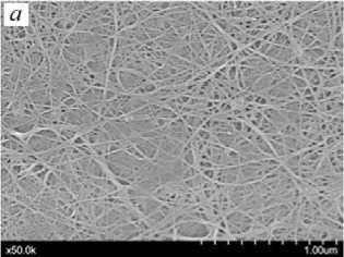
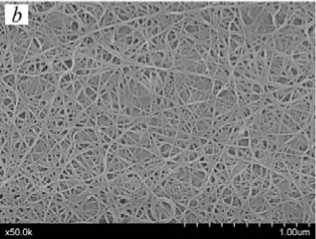
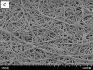
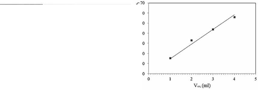
Fig. 1. SEM images of SWCNT films of various thicknesses: 1 ml ( a ) and 3 ml ( b and c ) of dispersion; TEM image of SWCNT films of various thicknesses: 1 ml ( d ) and 3 ml ( e ) of dispersion. Dependence of the SWCNT films thickness on the volume of sprayed dispersion ( f )
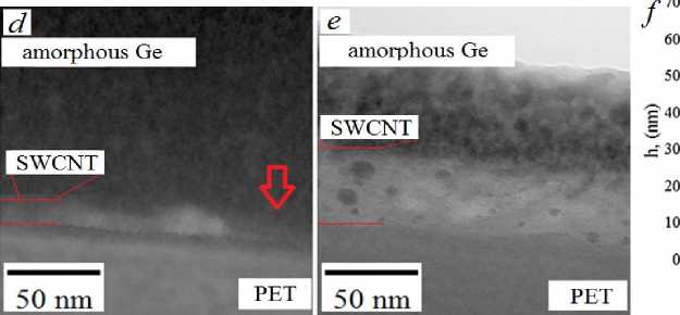
Рис. 1. СЭМ изображения пленок ОУНТ различной толщины: 1 мл ( а ) и 3 мл ( b и c ) дисперсии; ПЭМ изображение пленок ОУНТ различной толщины: 1 мл ( d ) и 3 мл ( e ) дисперсии. Зависимость толщины пленок ОУНТ от объема распыленной дисперсии ( f )
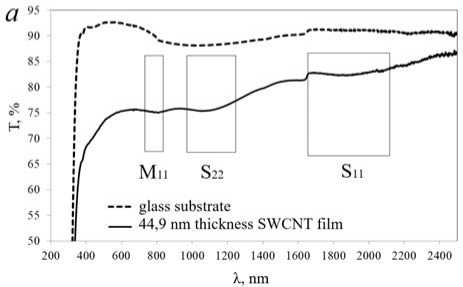
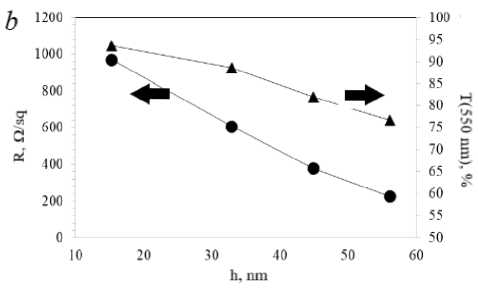
Fig. 2. Transmission of a SWCNT film 44.9 nm thick in the range 400–2500 nm ( a ); dependence of surface resistance and transmission of SWCNT films as a function of film thickness ( b )
Рис. 2. Пропускание пленки ОУНТ толщиной 44,9 нм в диапазоне 400–2500 нм ( а ); зависимость поверхностного сопротивления и пропускания пленок ОУНТ в зависимости от толщины пленки ( b )
Fig. 3 shows the Raman spectra for the films with thickness of 15.3 nm and 56.1 nm, obtained using a Horiba Jobin Yvon T64000 Raman spectrometer (Center of collective uses FRC KSC SB RAS).
Three peaks characteristic of SWCNTs can be distinguished in the spectra: the G-line characterizing the vibrations of the system of carbon sp2 bonds (~ 1592.8 cm–1) (graphite-like zone), the 2D line (~ 2678.7 cm–1), indicating two-dimensionality of the material, which is the overtone of the D-line (defective zone) (~ 1332.5 cm–1). The RBM peak (the breathing mode is a split peak at ~ 150.6 cm–1 and ~ 180.29 cm–1) characterizes expansion-compression vibrations relative to the central axis of nanotubes [12]. It is also worth noting that the film thickness does not affect the position of the peaks. The low intensity of the D mode indicates low defectiveness of the nanotube material; the ratio of the G / D peaks intensities is 23.4.
In [9] we calculated the diameter of SWCNTs of this type; it amounted to 1.6–1.8 nm, which correlates with the results of [13].
Fig. 5 shows the spectral dependences of the parameters S 11 and S 21 measured in dB which are reflection and transmission coefficients, respectively.
Thus, knowing the values of the coefficients S 21 and S 11 it is possible to calculate the transmission and reflection coefficients according to the following equations [14]:
T = Pt = 10(0.1 S 21 ), (1) P i
R = P r = 10 (0.1 S 11 ) .
P i
Fig. 3. Raman spectra of SWCNT films with thickness of 15 and 50 nm ( a ), enlarged fragments of D and G peaks ( b ) and RBM (radial breathing mode) ( c )
Рис. 3. Спектры комбинационного рассеяния пленок ОУНТ толщиной 15 и 50 нм ( а ), увеличенные фрагменты D и G пиков ( b ) и дыхательной RBM моды ( c )
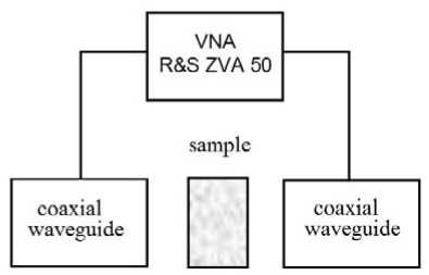
Fig. 4. Schematic representation of a measuring unit
Рис. 4. Схематическое изображение измерительной установки
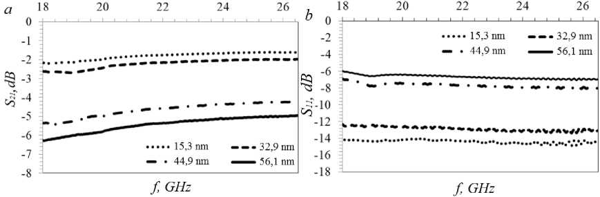
Fig. 5. Spectral dependences of parameters S 21 ( a ) and S 11 ( b ) for SWCNT films of various thicknesses
Рис. 5. Спектральные зависимости параметров S21 ( а ) и S11 ( b ) для пленок ОУНТ различной толщины
On the basis on the fact that the sum of all radiation components is 1, it is possible to calculate the fraction of absorbed radiation according to the following equation: A = 1 - T - R .
The dependence of transmission, reflection and absorption of SWCNT films of various thicknesses at the frequency of 18 GHz:
|
SWCNT film thickness, nm |
T (18 GHz), % |
R (18 GHz), % |
A (18 GHz), % |
|
15.3 |
60.8 |
4.1 |
34.6 |
|
32.9 |
54.8 |
5.8 |
39.4 |
|
44.9 |
29.2 |
20.4 |
50.4 |
|
56.1 |
23.6 |
25.2 |
51.2 |
The main model describing the relationship between the specific sheet resistances of thin films of nonmagnetic materials is the continuous layer model [14]
( 7.Л
SE ( dB ) = 20lg | 1 + -0- I . (2) I 2 R s )
Fig. 6 shows comparison of the experimentally obtained values of shielding efficiency at a frequency of 18 GHz from the sheet resistance of the coatings, calculated by the equation SE ( dB ) = - 10lg T of the surface resistance of SWCNT films at the boundaries of the studied range, and approximation of the experimental points by equation 2.
It can be seen from the graph that the results obtained are in agreement with the model, as a result of which it can be assumed that the shielding efficiency can be increased by reducing the surface resistance of SWCNT films. Single-walled carbon nanotubes can be doped and acquire either a hole [15] (doping with electron acceptors such as: HNO3, FeCl3, HAuCl4) or electron [16] conductivity (doping with electron donors: amines, phosphines, etc.). Initially SWCNT films have hole conductivity, as evidenced by the sign of the Seebeck coefficient (+40 mV at room temperature) [9]. As it can be seen from equation 2, lowering the sheet resistance due to doping to the value of 50 Ohm / sq helps to increase the shielding efficiency to the value of 13.5 dB or transmission of not more than 4.5 %, so the remaining 95.5 % of the power will be absorbed in the film and partially reflected back.
This fact indicates the promise of using transparent SWCNT films in solving the problem of shielding microwave electromagnetic radiation.
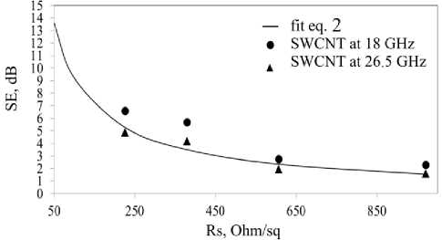
Fig. 6. Shielding efficiency as a function of sheet resistance for SWCNT films at the boundaries of the studied range
Рис. 6. Зависимость эффективности экранирования от величины поверхностного сопротивления для пленок ОУНТ на границах исследуемого диапазона
Conclusion: The electromagnetic shielding properties of thin SWCNT films on flexible PET (polyethylene terephthalate) substrates were studied. The contributions of reflection and absorption are determined. The absorption of radiation is the predominant factor in attenuation of radio emission in the studied K range (18–26.5 GHz). Increasing the film thickness from 15.9 nm to 56.1 nm increases the fraction of absorbed radiation from 34.6 to 51.2 % at the frequency of 18 GHz.
Acknowledgement. The work was supported by Russian Foundation for Basic Research, project «mol_a» № 18-38-00852.
References Research of electromagnetic shielding properties of single-walled carbon nanotubes thin transparent films
- Zhu M., Xiong C., Lee Q. Research on ITO transparent electromagnetic shielding coatings for E-O system. Proc. of SPIE. 2009, Vol. 6722, P. 1–7.
- Choi Y.-J., Gong S. C., Johnson D. C. et al. Characteristics of the electromagnetic interference shielding effectiveness of Al-doped ZnO thin films deposited by atomic layer deposition. Applied Surface Science. 2013, Vol. 269, P. 92–97.
- Xu H., Anlage S. M., Hu L., Gruner G. Microwave shielding of transparent and conducting single-walled carbon nanotube films. Applied Physics Letters. 2007, Vol. 90, P. 183119.
- Hong S. K., Kim K. Y., Kim T. Y. et al. Electromagnetic interference shielding effectiveness of monolayer grapheme. Nanotechnology. 2012, Vol. 23, P. 455704.
- Zhang H.-L., Xia Y., Gai J.-G. Ultrathin Active Layer for Transparent Electromagnetic Shielding Window. ACS Omega. 2018, Vol. 3, P. 2765–2772.
- Electromagnetic Interference (EMI) Transparent Shielding of Reduced Graphene Oxide (RGO) Interleaved Structure Fabricated by Electrophoretic Deposition / S. Kim, J.-S. Oh, M.-G. Kim et al. // ACS Appl. Mater. Interfaces. 2014, Vol. 620, P. 17647–17653.
- Kim B. R., Lee H. K., Kim E., Lee S. H. et al. Intrinsic electromagnetic radiation shielding/absorbing characteristics of polyaniline-coated transparent thin films // Synthetic Metals. 2010, Vol. 160, P. 1838–1842.
- Voronin A. S., Simunin M. M., Ivanchenko F. S. et al. Preparation and Investigation of Composite Transparent Electrodes of Poly (3, 4-ethylenedioxythiophene) Polystyrene Sulfonate/Single-Wall Carbon Nanotubes. Technical Physics Letters. 2017, Vol. 43, No. 9, Р. 783–786.
- Tambasov I. A., Voronin A. S., Evsevskaya N. P. et al. Structural and Thermoelectric Properties of Optically Transparent Thin Films Based on Single-Walled Carbon Nanotubes. Physics of the Solid State. 2018, Vol. 60, No. 12, P. 2649–2655.
- Volochaev M. N., Komogortsev S. V., Myagkov V. G. et al. Structural and Magnetic Characteristics of Nanogranular Co–Al2O3 Single- and Multilayer Films Formed by the Solid-State Synthesis. Physics of the Solid State. 2018, Vol. 60, No. 7, P. 1425–1431.
- Wu Z., Chen Z., Du X., J. M. Logan et al. Transparent, conductive carbon nanotube films. Science. 2004, Vol. 305, No. 5688, P.1273–1276.
- Dresselhaus M. S., Dresselhaus G., Saito R., Jorio A. Raman spectroscopy of carbon nanotubes. Phys. Rep. 2005, Vol. 409, No. 2, P. 47–99.
- Chortos A., Pochorovski I., Lin P. et al. Universal Selective Dispersion of Semiconducting Carbon Nanotubes from Commercial Sources Using a Supramolecular Polymer. ACS Nano. 2017, Vol. 11, P. 5660–5669.
- Wan Y.-J., Zhu P.-L., Yu S.-H. et al. Graphene paper for exceptional EMI shielding performance using large-sized graphene oxide sheets and doping strategy. Carbon. 2017, Vol. 122, P. 74–81.
- Hecht D. S., Hu L. B., Irvin G. Emerging Transparent Electrodes Based on Thin Films of Carbon Nanotubes, Graphene, and Metallic Nanostructures. Adv. Mater. 2011, Vol. 23, P. 1482–1513.
- Brownlie L., Shapter J. Advances in carbon nanotube n-type doping: Methods, analysis and applications. Carbon. 2018, Vol. 126, P. 257–270.
