Research on the method of multi-channel video acquisition and display based on FPGA

Author: Jingbo Xia, Xiaohuan Zhao, Weiwu Guo
Journal: International Journal of Computer Network and Information Security(IJCNIS) @ijcnis
Article in issue: 1 vol.2, 2010.
Free access
With the problems of high speed and asynchronism in a multi-channel video, a video monitor system based on FPGA and SRAM is designed and implemented. The system adopts the method of time-division multiplexing to realize the function of four-channel video parallel acquisition. The synchronization between four-channel video is achieved by using the field-selected algorithm. The four-channel video can be outputted to LCD with the technique of ping-pang cache. The LCD display sequences are generated by the finite state machine using Verilog HDL. The system is simple, flexible and with high-quality, and it has a broad application prospect.
Multi-channel video monitoring, time-division multiplexing, field-selected algorithm, ping-pang cache, finite state machine
Short address: https://sciup.org/15010981
IDR: 15010981
Text of the scientific article Research on the method of multi-channel video acquisition and display based on FPGA
Published Online November 2010 in MECS
As the most important method of acquiring information from the world, the video has been widely used in all kinds of places such as military battle, industry manufacturing, transportation and family living. One of the dominating characteristics of video is its huge data size which is a difficulty for video signal processing. It is necessary to promote system parallel processing ability with optimizing hardware and software structure to process video information in real-time.
Video monitoring is referred to the key techniques of video acquisition and display in video processing. It is required to acquire multi-channel video simultaneously in some occasion. The synchronization between different channel input signals is hardly to realize, so the multi-channel video monitoring always requires great efforts and skills. The high-quality cameras that can work in synchronization are adopted in [1] and the problems of dual cameras synchronization are settled by the meanings of external synchronization triggering signal. The panoramic surveillance is realized by using heterogeneous dual-core structure based on DSP+FPGA and multi-level ping-pang cache strategy in [2].
With the input signals are not synchronous between four analog CCD cameras, this paper adopts field-selected algorithm and time-division multiplexing technique to realize the functions of acquiring and display four-channel video simultaneously based on one ping-pang cache strategy on FPGA.
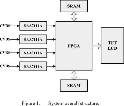
The overall video monitoring system structure is illustrated in Fig.1. The CVBS signal of the format of PAL is inputted and the four-channel independent RGB ( 5 : 6 : 5 ) signals are decoded by four SAA7111A chips. The four-channel videos are processed by FPGA. FPGA composes the four-channel videos and writes them in one buffer if the four-channel videos are required to display at the same time. When the single-channel video is required to display, FPGA gates corresponding video to the buffer. As the video acquisition and display both need strict clock synchronization, the strategy of two SRAM ping-pang cache structure is adopted by FPGA to realize the function of outputting the video on LCD continuously.
The LCD resolution is 640×480 in the system. The system both needs the function of display four-channel videos with the resolution of 320×240 and single-channel video with the resolution of 640×480 that controlled by external interrupt signal. Thus, two 512K×16bit SRAM are selected as buffers. Then, the logical elements and I/O pins should be sufficient for the system need when it is designed.
-
II. The overall module design of the video MONITOR SYSTEM
The common input methods of the FPGA design include schematic circuit diagram and hardware description language. The HDL method abides by the principle of up-to-down design and has the advantages of modular form and multiplexing, so it is easy to transplant. VHDL and Verilog HDL are the most used hardware description language at present. The Verilog HDL is adopted in the paper.
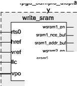
As illustrated in Fig.2, the process of the video monitoring is divided to the three modules which are fpga_sample_display, write_sram and read_sram.
-
(1) The top module of the system is fpga_sample_display and it is responsible for cooperating the parallel running of the video acquisition and video display. It calls the lower modules of write_sram and read_sram and generates the controlling signals such as rsram1_en, rsram2_en, wsram1_en and wsram2_en. Thus, the two SRAM are written and read in turn.
-
(2) The module of write_sram is the most important module in the video monitor syatem. The field-selected algorithm is applied in the module to realize the function of parallel acquiring the four-channel synchronous videos.
-
(3) The module of read_module is responsible for
fetching data from the two SRAM. The display time sequences of the TFT-LCD are generated in this module and the valid video data is outputted to the LCD controlled by these time sequences.
fpga_sample_displa rts0[1:4] I------>- href[1:4] | > vre^1:4] I >
Hc[1:4] I > vpo[1:4] | >■
write sram wsram2_en — sram2 nce_buf— sram2_addr buf —


lcd_vsyn lcd_fisyn lcd_Siabl read sram
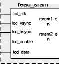
Figure 2. The inner modules of FPGA
Ш. Critical Principles in the modules of FPGA
-
A. The Principles of Ping-pang Cache in the module of fpga_sample_display
The acquisition and display of the four-channel videos are paralleling executed, so the ping-pang cache strategy is adopted [3]. FPGA generates all kinds of time sequences and refreshes data to LCD continually. The circuit of Fig.3 is able to fulfill the parallel operation [4].
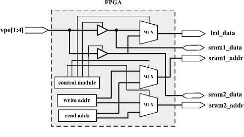
Figure 3. Ping-pang cache circuit
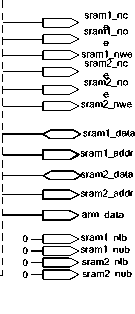
As illustrated in Fig.3, vpo[1:4] is connected to sram1_data and sram2_data via multi tri-state gate and sram1_data and sram2_data are connected to lcd_data through multiplexers. When it is the odd frame time, vpo[1:4] connects with sram1_data and disconnects with sram2_data through high impedance, and lcd_data connects with sram2_data. In the meantime, SRAM1 is at the write-state and SRAM2 is at the read-state. When it is the even frame time, vpo[1:4] connects with sram2_data and disconnects with sram1_data, and lcd_data connects with sram1_data. At this time, SRAM1 is at the read-state and SRAM2 is at the write-state. The address of SRAM is generated by the writing and reading modules of FPGA and SRAM can only receive one address at a time controlled by MUX.
The function of ping-pang cache is realized by the inner logic of the FPGA program. The following Verilog HDL codes illustrate the basic principles of the switch between two caches.
assign sram1_ce = frame? sram1_nce_wr : sram1_nce_rd; assign sram2_ce = frame? sram2_nce_rd : sram2_nce_wr; assign sram1_addr = frame? sram1_addr_wr : addr_read; assign sram2_addr = frame? addr_read : sram2_addr_wr; assign sram1_data = frame? sram1_data_buf : 16'bzzzzzzzzzzzzzzzz;
assign sram2_data = frame? 16'bzzzzzzzzzzzzzzzz : sram2_data_buf;
-
B. Field-selected Algorithm in the module of write_sram
The four channel signals are inputted in FPGA at the same time. Although FPGA has the ability of parallel processing, the four channel videos are required to be written in one buffer that is only able to receive or send one channel video at a time. Therefore, the four parallel signals are required to be converted to serial signal.
The four-channel video signals are decoded by the chip SAA7111A. The decoded video signals are at different phases but with the same frequency. It is able to use one global clock to capture the four signals if these signals are delayed to the same phases. The data is written to FPGA according to pixel clock and it is not lost if FPGA can fetch the current pixel before the next pixel is written. Therefore, the data can be stored on the four flip-latches of FPGA temporarily, and the global clock is responsible for fetching data in time. Thus, the four-channel videos can be handled in parallel ways [5].
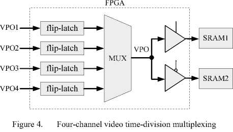
The principle of video acquisition is illustrated in Fig.4. The videos VPO1, VPO2, VPO3, VPO4 are written on the latch at each pixel clock, and FPGA fetch the data sequentially controlled by the global clock which frequency is the 8 times of any channel pixel clock. The data on the latch isn’t lost because the writing rate by VPO and the fetching rate by MUX are equal. The size of each latch is 16 bit that exactly holds one pixel data. The data acquisition of the four channels is separated by time slot but it is processed in parallel from macro-observation [6].
With the four-channel videos displayed at the same time, FPGA outputs data from buffers to the LCD corresponding with its address of LCD, and the writing four images are guaranteed to be complete before LCD refreshed every time. In fact, it is difficult to make sure the completeness of each channel video image because of the asynchronism of the input signals.
To avoid data collision on the single-port SRAM bus, the clock of VPO1 is selected as reference clock, and 8 periods of the reference clock called Mclk is a cycle of the State Machine [7-8]. Vpo1 is always written at the 1-2 Mclk, Vpo2 is written at the 3-4 Mclk, Vpo3 is written at the 5-6 Mclk and Vpo4 is written at the 7-8 Mclk. The signal F_sign is the switching signal between SRAM1 and SRAM2.
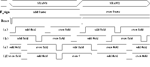
Figure 5. Possible time sequence of the video
field ||
The multi situations may be appeared illustrated in Fig.5 because of the asynchronism of the four-channel videos.
Fig.(a) illustrates an ideal synchronized state. When Frame is changing, the V_enable is at the vertical blanking interval, and the valid data of odd field and even field is at the half period of F_sign.
Three asynchronous situations are illustrated in Fig.(b)(c)(d). If (b)(c)(d) are required to be synchronized with (a), they should be delayed to 0~0.5 period of the F_sign. The resolution of one-channel video is 320×240, and 3 FIFO with the size of 320×240×16=1228800bit is required at the worst. The four-channel videos are 100% captured only when each FIFO is at the size of 1228800bit because the delay time of each channel video is uncertain. Obviously, mass of logic elements are wasted in this way.
As illustrated in Fig.5, there is a complete field data in the high or low period of F_sign at any situation. If the resolution of a field can meets system need, an appropriate field is can be selected to synchronize multi-channel video and no more logic elements are added. One field video in PAL format has 287.5 lines valid data and one line has 720 valid pixels. It is obvious that one field data can meets the demands of the system.
As illustrated in Fig.3, a complete field data between any two sequential fields can be found at the stage of writing one SRAM. Field-selected algorithm is responsible for selecting the complete field and writing it in SRAM [9]. The whole field-selected synchronous algorithm is shown as Fig.6.
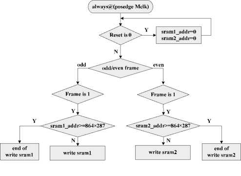
Figure 6. Field-selected synchronous algorithm
The Reset generates a transitory negative pulse when 1st new video is coming. The pixel_count that is the counter of video pixel is set to “0”, then the odd-even frame signal F_sign of is judged, and the SRAM1 is operated in the odd period, SRAM2 is operated in the even period. When each video enable signal V_enable such as (a)(b)(c)(d) is at the “high” lever, the pixel_count is judged first. If pixel_count>=864×287, it means a complete video has been written and SRAM needn’t be operated in the period of the frame time, otherwise SRAM is required to be written. In one frame time, pixel_count is cleared only once and a complete field data is always able to be found, so pixel_count can always reaches 864×287 in the period of a frame time. In sum, the synchronized four-channel videos with the resolution of 320×240 can be acquired in one frame time at any circumstance.
An ideal Reset should be generated a transitory negative pulse just when a new frame is coming, and its period should last a frame time as Fig.3. FPGA utilizes the signal Reset as frame synchronization signal and initializes the SRAM while “Reset=0” and writes the SRAM while “Reset=1”. In this way, SRAM1 write-module works in the odd frame and SRAM2 write-module works in the even frame. SRAM1 and SRAM2 are able to use one write-module with time-division multiplexing. Owing to sharing one write-module, FPGA saves 3814 logical elements accounting for abundant LE of FPGA.
-
C. the generation of time sequences of TFT-LCD in the module of read_sram
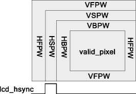
As illustrated in Fig.7, the video can display correctly only when the horizontal synchronization signal lcd_hsync, the vertical synchronization signal lcd_vsync, the pixel clock lcd_clk and the enabled signal lcd_enable are accurately generated. The region of the LCD is divided into several parts and only the data that corresponds with valid_pixel area can display on LCD. When the signals lcd_hsync and lcd_vsync are at the low period, the enabled signal lcd_enable is valid and the data can be outputted. When the signals lcd_hsync and lcd_vsync are at the blanking period, the enabled signal is disabled and the output data is permitted.
lcd_vsync
lcd_enabl e
Figure 7. The diagrammatic sketch of LCD display

Because the time sequence is complicated and highly precise, the finite state machine is used to generate the following sequences illustrated in Fig.8.
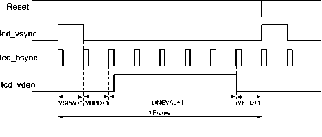
Figure 8. The generation of the sequence of lcd_vsync
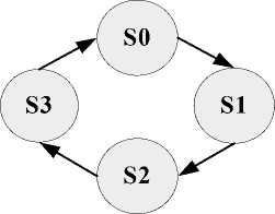
Figure 9. The transition of lcd_vsync states
-
(1) S0: the high period of the lcd_vsync. When the negative pulse of the Reset comes, a new frame is beginning. At this period, lcd_vsync=1 and lcd_vden=0. The lcd_hsync is counted form 0 to VSPW.
-
(2) S1: the period of vertical back scanning. At this period, the lcd_vsync=0 and lcd_vden=0 and cd_hsync is counted form 0 to VBPD.
-
(3) S2: the valid period of the frame. At this period, the lcd_vsync=0 and lcd_vden=1 and cd_hsync is counted form 0 to LINEVAL At this period, the lcd_vden is at the active state..
-
(4) S4: the period of vertical front scanning. At this period, the lcd_vsync=0 and lcd_vden=0 and cd_hsync is counted form 0 to VFPD.
The generation of the lcd_hsync is similar to the generation of the lcd_vsync, bur the lcd_hsync is counted at the frequency of lcd_clk. When the lcd_vden=1 and lcd_hden=1, LCD receives the data from the SRAM. Because of the differences of LCD, the front scanning time and the back scanning time always need to be adjusted to the time sequence of the LCD [11].
The finite state machine is implemented by Verilog HDL and the time sequences of TFT-LCD are simulated at the development environment of Quartus II 6.0. The Fig.10 shows that the time sequences of the LCD display are precise and correct.
The generation of the signal lcd_vsync is illustrated in Fig.8 [10]. In this process, four states S0, S1, S2 and S3 are necessary. The Fig.9 shows the transition of the four states.
J
и
Ш1ШШШШ1ШШШШМШ1Ш
I I I I I I I I I I I I I I П I П I I I I I I I I I I I I I I I i i 1 ill
I I I i I I I I I I il l I I I I I I I I I I I I I I I I I I I i i i i
ЛПЛПЛППЛЛЛППЛЛЛПЛППППЛЛЛЛЛЛПЛПП.
Figure 10. The simulated sequence of TFT_LCD
W. Conclusion
The input signals are four channel CVBS videos with the format of PAL, and the SHARP CORPORATION TFT-LCD with the resolution of 640×480 is used. The system should be automatically switched between the four-channel videos and one-channel video as illustrated
Fig.11. The experiment result indicates that the four-channel videos with the rate of 25 frame/second are able to be acquired simultaneity and the four-channel videos and any one-channel video can be automatically switched.
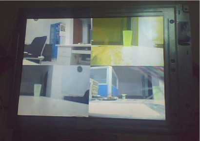
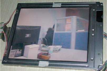
Figure 11. System test result
The techniques of time-division multiplexing, field-selected synchronization and ping-pang cache are adopted in the multi-channel video monitoring system, and the functions of multi-channel video monitoring acquisition and display are realized on one FPGA. With the input is four-channel colored composite video of PAL/NTSC format, the system can fluently acquire and display four or one channel video. The functions of background and video overlap are being added in further development, and it has a broad application prospect.
References Research on the method of multi-channel video acquisition and display based on FPGA
- HUO Ju, FU Liang, YANG Ming. Research on the structure of the dual cameras synchronization system for high speed image capture and storage[J]. Optical Technique, 2007, 33(1) :106-109.
- Chen Li-dong, Zhang Mao-jun, Wang Wei, et al. A Heterogeneous Dual-Core High-Speed Processing System for High Resolution Catadioptric Panorama[J]. Journal of Electronics & Information Technology, 2009, 31(4) :822-826.
- Cheng Zijing, Zhou Xiaokuan, Jiang Hongxu. Image Compression ASIC for Satellite Remote Sensing Application[J]. Journal of Beijing University of Aeronautics and Astronautics, 2003, 29(2) :151-155.
- CHEN Guo-jin, ZHU Miao-fen, SHI Hu-li. Image auto-focusing system based on field programmable gate array[J]. System Engineering and Electronics, 2008, 30(2) :209-212.
- Ma Xin, Guo Hong. Design of multi-slice CT data acquisition system and its measurement[J]. Journal of Beijing University of Aeronautics and Astronautics, 2008, 34(7) :794-797.
- Dang Jun-li, Liu Bai-yu, Ou-Yang Lan, et al. High Speed Electro-optic Gating System Design Based on FPGA[J]. Acta Photonica Sinica, 2009, 38(5) :1091-1095.
- WEI Ting-cun, GAO Wu. Research of One-chip TFT-LCD Driver IC[J]. RESEARCH & PROGRESS OF SSE, 2008, 28(2) :258-263.
- LIU Wei, ZHOU Yu-mei, YE Qing. Test Algorithm for Register File Memories[J]. RESEARCH & PROGRESS OF SSE, 2005, 25(1) :89-92.
- WEN Feng, DAI Ji-zhi, TANG Zun-lie, et al. Selected-frame Display Technology for High Frame CCD Camera[J]. Semiconductor Optoelectronics, 2008, 29(5) :782-784.
- ZHAO Xiao-huan, Xia Jing-bo, Zhao xu, et al. Design of Video Player Based on FPGA[J]. Video Engineering, 2010, 34(4) :52-55.
- XU Xiao-ru, ZHAO Meng-lian, Wu Xiao-bo. On-chip boost regulator with projected off- and on-time control[J]. Journal of Zhejiang University(Science A: An International Applied Physics & Engineering Jounal), 2009, 10(8) :1223-1230.
