Reversible Shift Counter Design on QCA

Author: Abhinay Choudhary, Snigdha Singh, Manoj Kumar Jain
Journal: International Journal of Modern Education and Computer Science @ijmecs
Article in issue: 11 vol.11, 2019.
Free access
In the Current scenario of higher level of integration the most encountered problems are heat dissipation and information loss on each and every computation. For the sake of eliminating these issues Reversible computing is being adopted as a preferable substitute of digital circuit design. This paper focuses on the design of Reversible Ring Counter and Twisted Ring Counter using Reversible D flip flop implemented with the Novel Design of Feynman and Fredkin Gate. Ring counters are commonly found in applications used to count the data in a continuous loop as well as in frequency divider circuits. While twisted (or Johnson) ring counter is used as three-phase square wave generators (using 3 flip-flops) and quadrature oscillator circuits (using 2 flip-flops) etc. The response of the proposed counter circuit is tested with the help of QCADesigner 2.0.3 simulation tool and the Energy dissipation is analyzed by the use of QCA Designer-E tool.
Quantum cost, garbage output, constant input, reversible logic, ring counter, twisted ring counter, D flip-flop
Short address: https://sciup.org/15017145
IDR: 15017145 | DOI: 10.5815/ijmecs.2019.11.06
Text of the scientific article Reversible Shift Counter Design on QCA
Published Online November 2019 in MECS DOI: 10.5815/ijmecs.2019.11.06
-
I. Introduction
For the sake of the development of the computing machines notable achievements have been made in the previous decades. In early 70s the computers were so bulky encompassing of thousands of components but now the demand of miniaturization has made the computers in such a modified way that billions of components can be mounted in a few millimeter of area. The founder of Intel, Gorden E. Moore in 1965[1] had predicted at that time and states that the number of transistor on chip doubles every 18 months and this prediction is valid up to current date. In future this exponential rise may lead to an
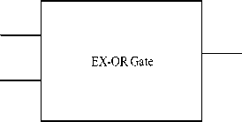
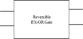
extreme situation due to the higher level of integration and a great deal of power dissipation. This power dissipation basically occurs in the form of heat which may destroy the silicon chip resulting in the reduced chip reliability. The higher degree of power dissipation is the major issue with the chip designing in this era of the compact and higher processing speed computers. The power dissipated was calculated by R Launders’s [2, 3] as kT ln2. For the reduction in the dissipated power an effective substitute is the bijective nature of digital Logic given by C.H. Bennett [4]. Reversible logic is a promising substitute in this direction because computations can be reverted in this case. On considering a very basic AND logic if the output is 1 then we can easily predict the input set to be (1, 1), in the other possible output set i.e. 0 an ambiguity rises in the output set (0, 0) (0, 1) (1, 0). Thus, the conventional logic is inefficient in the way of input recovery from output vector. Now on considering the conventional EX-OR gate truth table, we can easily visualize that in case output is 1 input vector maybe (0, 1) or (1, 0). Thus we can observe the bit overlapping in the case of conventional design, for removing these demerit additional bits is required which is numerically expressed as log2 ц where, Ц is the maximum number of time output is being overlapped. In case of EX-OR Gate, output overlapping is 2 resulting in additional output log2 2 = 1 . By adding an additional output bit conventional Ex-OR may be converted to a reversible EX-OR gate shown in Table 1.
On the other hand if the logic is reversible in nature like a very basic Feynman gate (Reversible EX-OR gate) input and output are faithfully recoverable from each other and not a single condition of ambiguity or bit overlapping occurs in input-output vectors. The block diagram of EX-OR and reversible EX-OR gate is depicted in fig.1.
Table 1. Truth table of (a) EX-OR gate (b) Reversible EX-OR gate
|
A |
B |
F |
|
0 |
0 |
0 |
|
0 |
1 |
1 |
|
1 |
0 |
1 |
|
1 |
1 |
0 |
|
A |
B |
P=A |
Q=A ⊕ B |
|
0 |
0 |
0 |
0 |
|
0 |
1 |
0 |
1 |
|
1 |
0 |
1 |
1 |
|
1 |
1 |
1 |
0 |
(a) (b)
From above we can define Reversible Logic [5, 6] as a digital logic consisting of equal number of elements in input and output vector holding the bijective nature which implies one to one mapping between input and output vectors .
A
B
A ⊕ B
(a)
A
B
P=A
Q=A ⊕ B
(b)
Fig.1. Block Diagram of (a) Conventional EX-OR Gate (b) Reversible EX-OR gate
The remaining paper is arranged as section II explains the basic key terms related to Reversible Logic, section III focuses basically on conventional ring as well as twisted ring counter. The proposed Reversible shift counter is illustrated in section IV along with schematic and result discussion in section V. Conclusion and future Scope is explained finally in section VI.
-
II. Key Terms
This section has brief some of the important key terms which are frequently raised in the literatures. These terms help to design more efficient reversible logic circuits, if the designer will take in consideration in his design. These are:
V * V = NOT(1)
V + *V + = NOT(2)
V * V + = V + *V = 1
In other words area * latency 2 in QCA [9, 10, 11, 12] also yields the circuits Quantum cost [13].
Latency can be defined as the number of clock zones used in the critical path.
-
III. Conventional Design
Shift counter can be defined as a synchronous counter arranged in the shift register form. The bit transfer occurs either from left to right or right to left on the application of clock signal. Shift counter can be constructed by the adjacent linking of D flip-flops [14]. On the basis of the feedback fed to the input terminal of first D flip flop shift counter can be categorized as: ring counter and twisted ring counter.
Ring Counter:
Ring Counter also known as straight ring counter or one hot counter is a synchronous counter consisting of four D flip flops arranged in such a way that output of each stage is fed as input to next stage and the final stage output is connected to the input of first stage and preset is set high(fig.2.). Single 1 moves in the loop or ring that’s why named as ring counter or one hot counter. It’s truth table is shown in table 2.
Twisted Ring Counter:
Johnson counter or Twisted Ring Counter [15, 16] is very similar to ring counter in construction containing of four back to back D flip flop in SISO shift register form, the only difference lies in the connection of first flip flop input to be complement of output of last flip flop instead of the un-complemented or by default output as shown in fig.3. In terms of number of flip flop being used it is quite efficient than that of the ring counter because it requires half of the flip flop than the ring counter in case of similar counting sequence. It’s truth table is illustrated in Table 3.
Constant inputs/Ancilla inputs: Constant Input can be defined as the predefined input values while Reversible circuit designing.
Garbage output: Garbage output [7] is the additional output terminal used as an add-on in such a way that the input and output vector become equal in number .
Quantum Cost: The number of primitive gates i.e. NOT, CNOT, V and V + used for the motive of circuit designing is termed as its quantum cost [8] holding below axioms:
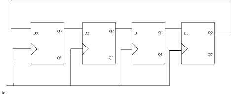
Fig.2. Conventional Ring Counter
Table 2. Conventional Ring Counter Truth Table
|
Clock |
Q3 |
Q2 |
Q1 |
Q0 |
|
1 |
1 |
0 |
0 |
0 |
|
2 |
0 |
1 |
0 |
0 |
|
3 |
0 |
0 |
1 |
0 |
|
4 |
0 |
0 |
0 |
1 |
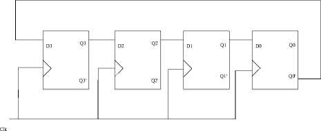
Fig.3. Conventional Twisted Ring Counter
Table 3. Conventional Johnson Counter Truth Table
Feynman gate is acting as buffer and Fredkin Gate is simply by-passing the input signal D at the output which is the condition for the D Flip Flop.
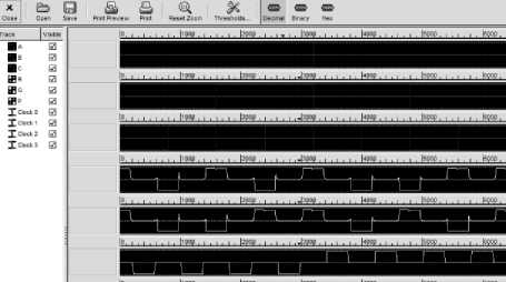
A novel optimized approach that has been used for implementation of Fredkin and Feynman gate in this paper has not been published earlier in any journal to the author’s knowledge. The schematic of Fredkin and Feynman proposed gates are illustrated in Fig.5 and output waveforms of these gates are shown in Fig.6 which is simulated by using QCADesigner tool.
(a)
(b)
|
Clock |
Q3 |
Q2 |
Q1 |
Q0 |
|
0 |
0 |
0 |
0 |
0 |
|
1 |
1 |
0 |
0 |
0 |
|
2 |
1 |
1 |
0 |
0 |
|
3 |
1 |
1 |
1 |
0 |
|
4 |
1 |
1 |
1 |
1 |
|
5 |
0 |
1 |
1 |
1 |
|
6 |
0 |
0 |
1 |
1 |
|
7 |
0 |
0 |
0 |
1 |
Fig.5. Schematic on QCA (a) Fredkin Gate (b) Feynman Gate
(a)
-
IV. Proposed Design
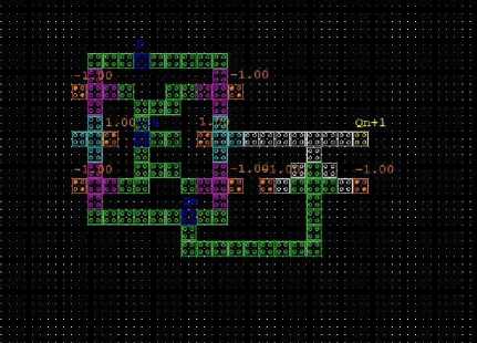
The conventional D flip flop has the demerit of information loss in case of bit manipulation i.e. whenever an input bit manipulation occurs then the input data is set to zero which results in the information loss of the circuit. This demerit gave rise to the idea of Reversible D Flip Flop[17]. The combination of Fredkin and Feynman Gate is being adopted here. The proposed Design of reversible D Flip Flop [18] is shown in fig.4.
|
Clk D |
— |
Fredkin Gate |
G1 G2 |
Q |
||
|
— |
0 |
Feynman Gate |
— |
Fig.4. Reversible D Flip Flop using Feynman and Fredkin Gate
Feynman gate is being used for the compensation of the feedback limitation. In the above block diagram
(b)
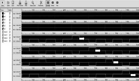
Fig.6. Waveform on QCA (a) Fredkin Gate (b) Feynman Gate
Table 4 and Table 5 presents the QCA layout comparison between the exiting design [19] and the proposed design of the Fredkin and Feynman gate respectively.
Table 4. Fredkin Gate layout comparison on QCA
|
No. of Cells |
No. Of Clock Zones Used |
Area |
|
|
Existing Design[19] |
121 |
4 |
0.16 |
|
Proposed Design |
72 |
3 |
0.08 |
|
Improvement |
40% |
25% |
50% |
Table 5. Feynman Gate layout comparison on QCA
|
No. of Cells |
No. Of Clock Zones Used |
Area |
|
|
Existing Design[19] |
83 |
4 |
0.10 |
|
Proposed Design |
18 |
2 |
0.02 |
|
Improvement |
78.3% |
50% |
80% |
(a)
Fig.7 shows that the schematic of reversible D FlipFlop (which employed Feynman and Fredkin gate) and the output waveform of proposed D Flip-Flop.
(a)
(b)
(b)
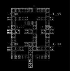
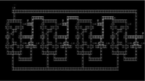
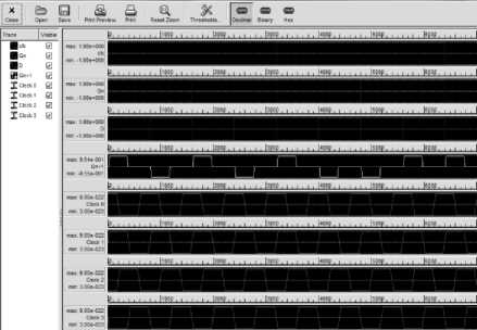
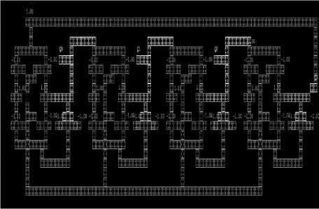
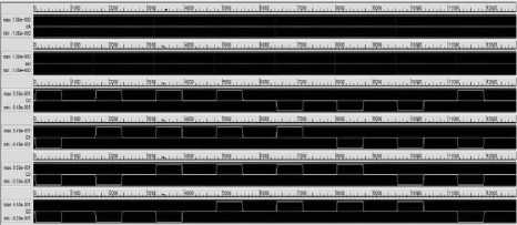
Fig.8. Reversible Ring Counter (a) Schematic (b) waveform
(a)
Fig.7. Reversible D Flip Flop (a) Schematic (b) Waveform
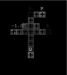
On cascading four reversible D flip flop and on connection of output of last stage with the input of first stage Reversible Ring counter is obtained, its schematic and waveform on QCA are shown in fig.8. On the other hand connection of the Complemented Output of last stage with the input of first stage twisted ring counter is obtained and the schematic and waveform of twisted ring counter are shown in fig.9.
(b)
Fig.9. Reversible Twisted Ring Counter (a) Schematic (b) waveform
Energy Dissipation Calculation of Reversible Ring Counter and Twisted Ring Counter:
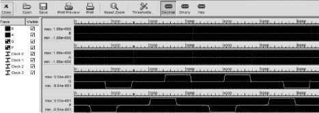
Energy dissipation can be calculated using QCA Designer-E[20] on considering the parameters shown in fig.10.
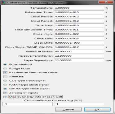
Fig.10. QCADesigner-E coherence vector Energy option
QCADesigner-E is actually simulation module of QCA Designer, the parameter description can be seen from data sheet [21].The simulation result display on enabling the option of display energy info of each cell in the coherence vector simulation shown below:
Reversible Ring Counter:
Sum_bath: : S 2.27e-001
S -2.02e-002
bE
Avg_bath: A 2.06e-002
A -1.84e-003
bE
Sum_clk: S -2.30e-001,
Avg_clk: : A -2.09e-002
Reversible Twisted Ring Counter:
Sum_bath: S 2.24e-001
S -2.00e-002
bE
Avg_bath: A 2.24e-001
A -1.82e-003
bE
Sum_clk: S -2.28e-001,
Avg_clk: A -2.07e-002
Where, S is the sum of all energy transfers to the bath during the whole simulation and S is the related error. and A , A are the average values of the energy transfers to the bath and the error for each clock cycle. S is the sum of the energy transfer to/from the clock during the whole simulation, while A is the average energy transfer during a clock cycle.
The above result confirms that the proposed circuits’ energy dissipation level is low.
-
V. Conclusion
This paper presents the design of Ring counter and twsited ring counter on QCA by adoting a Reversible D Flip Flop for circuit designing. This work can be taken as a nice step in sequential reversible circuit Designing.The proposed work can be used in the application in frequency division, 3 phase square wave generator, synchronous decade counter and Quadrature oscillator etc. The proposed design can be improved by lowering the clock zones and crossovers used.
References Reversible Shift Counter Design on QCA
- Gordon E. Moore," Cramming more components onto integrated circuits,"Electronics, volume 38, number8, April 19, 1965.
- R. Landauer, "Irreversibility and Heat Generation in the Computing Process," in IBM Journal of Research and Development, vol. 5, no. 3, pp. 183-191, July 1961.
- W. Keyes & R. Landauer,“Minimum Energy Dissipation in Logic,” IBM Journal of Research and Development. 14. 152-157. 1970.
- C. H. Bennett," Logical Reversibility of Computation," IBM Journal of Research and Development, vol. 17, no. 6, pp. 525-532, Nov. 1973.
- Snigdha Singh, Abhinay Choudhary, Manoj Kumar Jain, "A Brief Overview of Reversible Logic gate and Reversible Circuits," International journal of Electronics Engineering, volume 11,Issue 2 June - Dec 2019 pp.. 86-104.
- Jadav Chandra Das and Debashis De," Optimized Design of Reversible Gates in Quantum Dot-Cellular Automata: A Review," Reviews in Theoretical Science Vol. 4, pp. 1–7, 2016.
- Robert Wille, Rolf Drechsler, "Towards a Design Flow for Reversible Logic," Springer book.
- M. Surekha," Efficient Approaches for Designing Quantum Costs of Various Reversible Gates," International Journal of Engineering Studies. ISSN 0975-6469 Volume 9, Number 1 (2017), pp. 57-78.
- Craig S Lent, P Douglas Tougaw, Wolfgang Porod and Gary H Bernstein," Quantum cellular automata," Nanotechnology 4 (1993) 49-57. Printed in the UK.
- Craig. S. Lent, P. Douglas Tougaw, and Wolfgang Porod," Quantum Cellular Automata: The Physics of Computing with Arrays of Quantum Dot Molecules," 0-8186-6715-Xl94 $4.00 0 1994 IEEE.
- K. Walus and G. A. Jullien," Design Tools for an Emerging SoC Technology: Quantum-Dot Cellular Automata," in Proceedings of the IEEE, vol. 94, no. 6, pp. 1225-1244, June 2006.
- Massimo Macucci," Quantum Cellular Automata (QCA) Theory, Experimentation and Prospects," Copyright © 2006 by Imperial College Press ISBN 1-86094-632-1Printed in Singapore by World Scientific Printers (S) Pie Ltd.
- Md. Abdullah-Al-Shafi, Riasaad Haque Aneek , Ali Newaz Bahar," Universal Reversible Gate in Quantum-Dot Cellular Automata (QCA): A Multilayer Design Paradigm," International Journal of Grid and Distributed.
- G. Sushma and V. Ramesh, "Low power high speed D flip flop design using improved SVL technique," 2016 International Conference on Recent Trends in Information Technology (ICRTIT), Chennai, 2016, pp. 1-5.
- Sudheer, A & Ravindran," AjithDesign of Johnson Counter Using Embedded Logic Flip-Flop in 180nm Technology, International Conference on Recent Trends in Engineering, Technology and Management 2014.
- Abhishek Rai, Rajesh Mehra," Optimized Design and Simulation of 4-Bit Johnson Ring Counter Using 90nm Technology” International Journal of Research in Advent Technology, Vol.6, No.6, June 2018 E-ISSN: 2321-9637 Available online at www.ijrat.org
- S. Ranjith, T. Ravi, V. Kannan," Fault Tolerant Reversible Logic D-Flip Flop Based Shift Registers In 32nm CMOS Technology," International Journal of Engineering Research & Technology (IJERT) Vol. 2 Issue 2, February- 2013 ISSN: 2278-0181.
- G. C. Naguboina and K. Anusudha, "Realization and Synthesis of Ring Counter and Twisted Ring Counter Using Reversible Logical Computation with Minimum Quantum Cost," 2018 International Conference on Inventive Research in Computing Applications (ICIRCA), Coimbatore, 2018, pp. 926-931.
- F. Sill Torres, R. Wille, P. Niemann and R. Drechsler, "An Energy-Aware Model for the Logic Synthesis of Quantum-Dot Cellular Automata," in IEEE Transactions on Computer-Aided Design of Integrated Circuits and Systems, vol. 37, no. 12, pp. 3031-3041, Dec. 2018.
- Shaik Shabeena and Jyotirmoy Pathak," Design and Verification of Reversible Logic Gates using Quantum Dot Cellular Automata," International Journal of Computer Applications (0975 – 8887) Volume 114 – No. 4, March 2015.
- Manual for QCADesigner-Energy (QD-E) Manual version: 1.0(https://github.com/FSillT/QCADesigner-E)
