Simulation and Optimization of VHDL code for FPGA-Based Design using Simulink

Author: Naresh Grover, M.K.Soni
Journal: International Journal of Information Engineering and Electronic Business(IJIEEB) @ijieeb
Article in issue: 3 vol.6, 2014.
Free access
Simulations and prototyping have been a very important part of the electronics industry since a very long time. In recent years, FPGA's have become increasingly important and have found their way into all kind of digital system design This paper presents a novel, easy and efficient approach of implementation and verification of VHDL code using Simulink and then to regenerate the optimized VHDL code again using Simulink. The VHDL code written for the complicated digital design of 32-bit floating point arithmetic unit has been synthesized on Xilinx, verified and simulated on Simulink. The same VHDL code in Modelsim was optimized using this approach and the optimized code so generated by Simulinkhas also been synthesized to compare the results. Power dissipations for both synthesized designs using Xilinx Power Estimator were also extracted for comparison.
Modelsim, Simulink, Simulation, Optimization
Short address: https://sciup.org/15013251
IDR: 15013251
Text of the scientific article Simulation and Optimization of VHDL code for FPGA-Based Design using Simulink
Published Online June 2014 in MECS
Technologically, the basics of FPGA are the same as in most digital computing technology. The capacity, though, has increased tremendously. The amount of logical operations that a chip can contain, measured in the number of logical gates on the chip, has increased from a few thousand to millions. Even though the final product is a hardware component, the design and implementation of an FPGA-based system has strong similarities with software-based systems. A number of hardware description languages (HDL) or higher-level languages rather similar to software programming languages are typically used. This, together with the automated design tools, makes it very easy to define very complex functions. The steps of design use software tools to transform the design from one representation to another. The final output of the design process before configuring an actual device is a binary configuration code. FPGA device vendors have their own IDE (integrated development environment) tools that typically support at least the different design steps and simulation testing.
Despite the similarities with software design, aspects of hardware design must be understood by the designer. The levels of abstraction that a software-based system offers are not present in FPGA design. There is no system level or an operating system behind which the hardware issues are hidden. On the other hand, the complexity caused by the shared computing environment and interaction with other programs is absent. With both hardware and software aspects present, FPGA design and implementation can be characterized as “hardware implementation designed like software.”It is quite commonly agreed in the literature that, for applications with strict reliability and safety requirements, a design life cycle similar to software should be used.
In recent years, FPGA’s have become increasingly important and have found their way into digital system design.Efficient realization of any digital system using computation intensive algorithm is the combined effort of the adopted design methodology, optimization techniques and the targeted FPGA technology. Several design optimization techniques exists in literature which could be employed in FPGA-based design to realize efficient hardware. FPGA resource usage is an important measure of hardware cost (besides path delay and power consumption) [1].
Different techniques like pipelining, parallel processing and register balancing are employed to improve the maximum clock frequency, throughput and latency of the design. Techniques like resource sharing [2] and proper reset strategy [3] are employed to achieve area-optimal design. Itis very important to use design techniques that results in power efficient FPGA designs [4]. The various techniques like clock gating [5], asynchronous design [6], reducing clock speeds [7] etc. are used to optimize power.
This paper presents a novel approach of implementation and verification of VHDL code using Simulink and then to regenerate the optimized VHDL code again using Simulink. The VHDL code written for the complicated digital design of 32-bit floating point arithmetic unit [8]has been verified and simulated on MATLAB after synthesizing the same on Xilinx,The test bench was created for optimization through Simulink and optimized code so generated was again synthesized on Xilinx.The results of both in respect of device utility and power dissipation have been compared and presented.
The section II of the paper describes the Simulink model used for verification of VHDL code in Modelsim with its design steps, code device summary and codepower dissipation of VHDL code written for the complicated digital design of 32-bit floating pointarithmetic unit and finally depicts the simulation results. Section III of this paper presents the test bench model generated in Simulink for optimization and the sub-model created for this model. The device summary and power dissipation of theoptimized code have then been presented in the same section. The comparative report of various parameters for the original code and optimized code has been presented in Section IV and theconcluding remarks along with future scope have been finally presented in the Section V of this paper.
-
II. Verification Of Vhdl Code Using Matlab
Verification of VHDL code using Simulink of MATLAB requires compatible versions of MATLAB / Simulink and HDL Simulator ‘Modelsim’ to be loaded on the same system. The basic design steps to create Simulink model for verification of VHDL code in Modelsim HDL Simulator is shown in the work flow chart of Figure 1.

Create Writable folder outside MATLAB
Create vhdl code using Modelsim in new folder
Start MATLAB and launch Cosimulation Wizard
_
Specify Cosimulation type 'Simulink' and HDL Simulator option ’Modelsim’
Add vhdl code to HDL file list and specify compilation commands
Specify HDL module for cosimulation
Specify Input I Output ports of vhdl code
Set Clock, Reset values and HDL start time
End Cosimulation Wizard
Use generated HDL Cosimulation Block to launch 'modelsim'
Modelsim Simulator from Simulink as shown in Figure 3.
9 eject
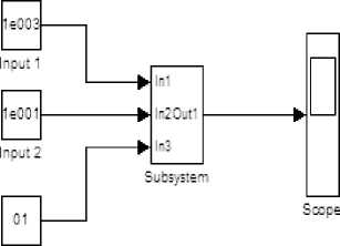
Fig.2: Simulink model to generate and verify Floating Point Arithmetic
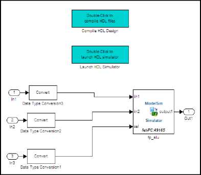
Fig.3: Simulink sub-systems to launch HDL Simulator
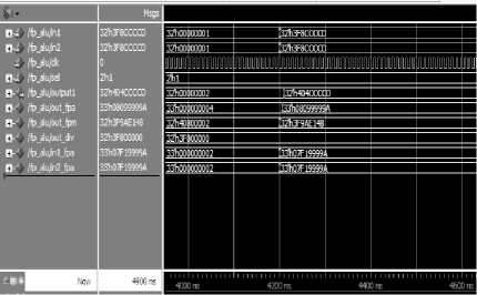
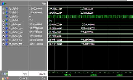
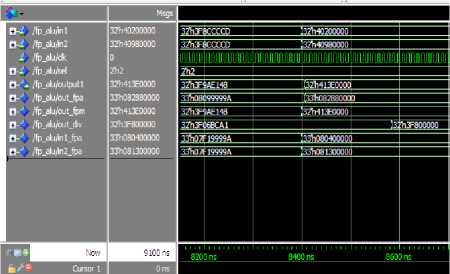
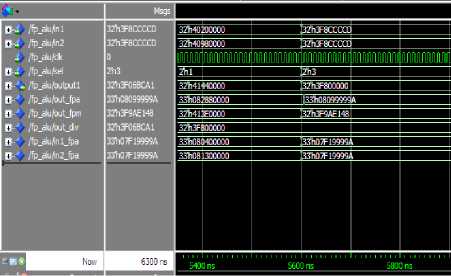
Double clicking the ‘Launch HDL Simulator’ in the Simulink model loads the test bench for simulation. The ModelSim Simulator opens a display window for monitoring the simulation as the test bench runs. The wave window in Figure 4 shows the simulation of two exponential inputs and Select set to ‘01’for ‘adder’ result as HDL waveform. Figure 5 shows the simulation of two decimal inputs for ‘adder’. Figure 6 and 7 show the simulation of two decimal inputs for ‘divider’. Figure 8 and 9 show the simulation of two decimal inputs for ‘multiplier’.
Run Cosimelation and verify vhdI code

Fig.1: Design steps to create Simulink model for verification of VHDL code in Modelsim
The Simulink Model to generate and verify Floating Point arithmetic created is shown in Figure 2. Input 1 and Input 2 are the two 32 bit floating point inputs to the model and ‘Select’ is set to ‘01’ for Adder, ‘11’ for Divider and ‘10’ for Multiplier. It also has a scope to view the output. A sub-system is created to launch the
Xilinx ISE 8.1 has been used as synthesis tool for VHDL program written for 32-bit floating point arithmetic unit as presented in [8] with a Virtex 4 as target device. The device utility summary and timing summary has been depicted in figure 10.
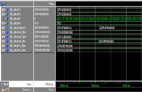
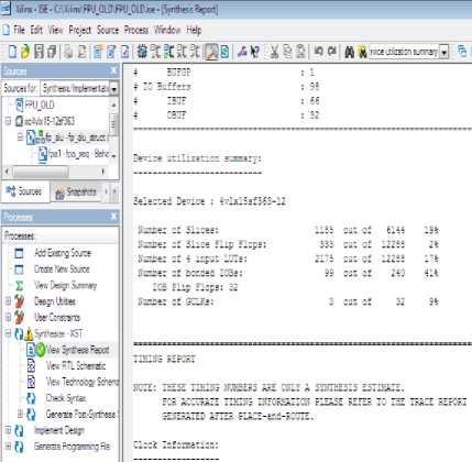
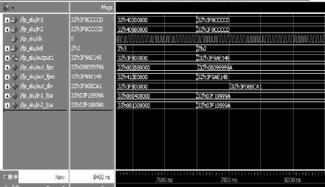
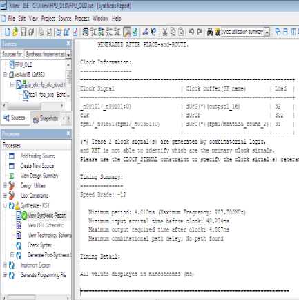
Fig.10: Device Utilization Summary Report and Timing Summary of initial VHDL code 32-bit Floating Point Arithmetic Unit
Code Power Evaluation
Power has been estimated using the Xilinx Power Estimation at the synthesis phase of the design cycle so that power estimation can be observed. The XPower Estimator Report for the 32-bit Floating Point Arithmetic Unit VHDL code has been depicted in Figure 11.
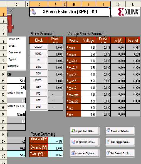
Fig.11: The XPower Estimator Report for the 32-bit Floating Point Arithmetic Unit un-optimized VHDL
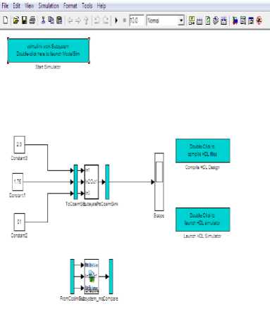
Fig.12: Test bench model in Simulink for optimization
-
III. Test Bench Model In Simulink For Optimization
For implementing a test bench, the design in linked with a subsystem block and test bench is applied as shown below:
Test Bench
Entity Subsystem_tb
Package Subsystem_tb_data
Package Subsystem_tb-pkg
Entity Subsystem

Entity Subsystem_tc Entity fp_alu
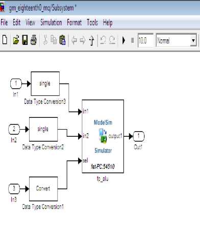
The test bench model generated in Simulink for optimization and the sub-system created for the model has been shown if Figure 12 and Figure 13 respectively.
Fig.13: Sub-system for Optimization
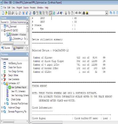
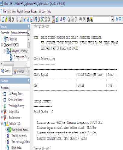
Fig.14: Device Utilization Summary Report and Timing Summary of Optimized VHDL code 32-bit Floating Point Arithmetic Unit
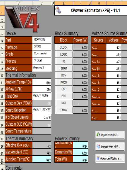
Fig.15: The XPower Estimator Report for the 32-bit Floating Point Arithmetic Unit VHDL
-
IV .Comparison
The results of implementation of the novel approach of optimization using MATLAB of the VHDL code of complicated digital design of 32-bit floating point arithmetic unit have been compared for the original initial code with the optimized code in respect of various parameters and have been tabulated in Table1.
Table1: Comparison of Parameters for Initial and Optimize code
|
S. No. |
Parameters |
Initial Code |
Optimized Code |
|
1 |
Number of Slices |
1185 out of 6144 19% |
422 out of 6144 6% |
|
2. |
Number of Slice Flip Flops |
333 out of 12288 2% |
332 out of 12288 2% |
|
3 |
Number of 4 input LUTs |
2175 out of 12288 17% |
781 out of 12288 6% |
|
4 |
Number of bonded IOBs |
99 out of 240 41% |
102 out of 240 42% |
|
5 |
Number of GCLKs |
3 out of 32 9% |
1 out of 32 3% |
|
6 |
Minimum period |
4.813ns |
4.813ns |
|
7 |
Maximum Frequency |
207.788MHz) |
207.788MHz) |
|
8 |
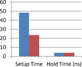
Minimum input arrival time before clock (Setup Time) |
48.274ns |
23.523ns |
|
9 |
Maximum output required time after clock (Hold Time) |
4.007ns |
3.935ns |
|
10 |
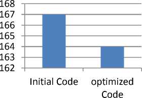
Power |
167mW |
164mW |
The following bar charts depicts the saving in number of slices, flip flops, LUTs and GCLKs after optimization in Figure 16 (a), the minimum input arrival time before clock and maximum output required time after clock in Figure 16 (b) and power estimated in Figure 16 (c).
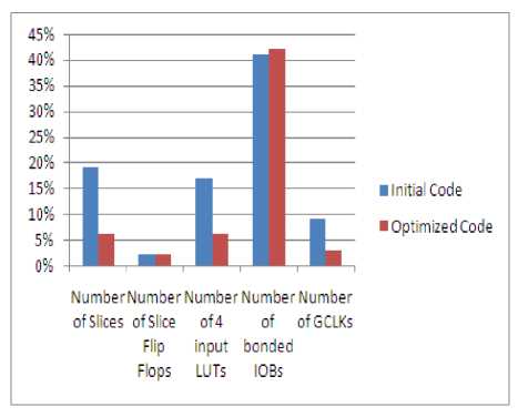
Fig.16(a): Bar Chart- Comparison of Parameters of original and optimized code
-
■ Initial Code
-
■ Optimized
Code
and power.
(ns)
Fig.16(b): Bar Chart- Comparison of Parameters of original and optimized code
Power (mW)
-
■ Power (mW)
Fig.16(c):Bar Chart- Comparison of Parameters of original and optimized code
References Simulation and Optimization of VHDL code for FPGA-Based Design using Simulink
- Shi, C., Hwang, J., McMillan, S., Root, A., and Singh, V.,"A System Level Resource Estimation Tool for FPGAs",International Conference on Field Programmable Logic and Applications (FPL), 2004.
- Xilinx Inc., Synthesis and Simulation Design Guide. June 2008.
- P. Garrault and B. Philofsky, "HDL Coding Practices to Accelerate Design Performance," Xilinx White Paper, wp231, pp. 1–22, Jan 2006
- F. Li, D. Chen, L. He, and J. Cong, "Architecture evaluation for power–efficient FPGAs," Proc.OftheACM/SIGDAInternational.Symposium onFieldProgrammable Gate Arrays, Feb. 2003,pp.175–184.
- Y. Zhang, J. Roivainen, and A. Mammela, "Clock–Gating in FPGAs: ANovel and Comparative Evaluation," Proc. of 9th EUROMICRO Conf.on Digital System Design (DSD'06), 2006, pp. 584–590.
- R. Manohar, "Reconfigurable asynchronous logic," Proc. of IEEE Custom Integrated Circuits Conf., Sept. 2006, pp. 13–20.
- ActelCorp.,"Designing for low power in ActelAntifuseFPGAs,"Application Note AC140, pp. 1–8, Sept. 2000.
- Naresh Grover, M.K.Soni," Design of FPGA-based 32-bit Floating Point Arithmetic Unit and verification of its VHDL code using MATLAB" IJIEEB, MECS pp 1-14, Jan 2014.
- Simulink HDL Coder 1; User's Guide; 2006-2010 by the MathWorks, Inc.
- Hikmat N. Abdullah and Hussein A. Hadi "Design and Implementation of FPGA Based Software Defined Radio Using Simulink HDL Coder". Engineering and Technology Journal, Iraq, ISSN 1681-6900 01/2010; Vol.28 (No.23):pp.6750-6767.
- R. Nanda, C.H. Yang and D. Markovic "DSP Architecture Optimization in MATLAB/Simulink Environment" in Proceedings International Symposium VLSI Circuits June 2008 pp 192-193.
