Simulation of a ballistic SW-CNTFET with coaxial geometry: numerical approach to determine the impact of gate oxide thickness on the performance

Author: Debashish Pal, Soumee Das
Journal: International Journal of Image, Graphics and Signal Processing @ijigsp
Article in issue: 6 vol.11, 2019.
Free access
Carbon Nanotube Field Effect Transistors (CNTFETs) are being proposed as candidates for next-generation integrated circuit technology replacing conventional MOSFET devices. It is a suitable nanoelectronic device which is used for high speed and low power design applications which include analog and digital circuits. In this paper, a single wall carbon nanotube field effect transistor (SW-CNTFET) with a coaxial structure in the ballistic regime has been studied and its performance parameters discussed. Numerical simulations were performed based on Natori approach. The various device metrics in consideration are drive current (Ion), Ion/Ioff ratio, output conductance (gd), trans-conductance (gm), gain, carrier injection velocity, sub-threshold swing and drain induced barrier lowering (DIBL). In particular, the influences of gate oxide thickness on the short-channel effects are presented in detail. Also, the dependence of sub-threshold swing and DIBL on the gate control parameter has been discussed.
Carrier Injection Velocity, Chirality, CNTFET, DIBL, Drive Current, Natori Approach, Short Channel Effect, Sub-threshold Swing, Tight Binding Energy, Trans-conductance
Short address: https://sciup.org/15016060
IDR: 15016060 | DOI: 10.5815/ijigsp.2019.06.04
Text of the scientific article Simulation of a ballistic SW-CNTFET with coaxial geometry: numerical approach to determine the impact of gate oxide thickness on the performance
Published Online June 2019 in MECS DOI: 10.5815/ijigsp.2019.06.04
In the near future, Si-based conventional MOSFETs are expected to be replaced by CNTFETs because of downscaling limitations associated with conventional bulk MOSFETs. Scaling of channel length below 10nm in conventional MOSFETs has severely impaired their performance due to the increase of short channel effects like sub-threshold swing (SS), drain induced barrier lowering (DIBL) and threshold voltage roll-off [1]. CNTFET nanotransistors have emerged as promising alternatives to replace the existing technological limitations imposed due to channel length shortening. CNTFET offers the following advantages over bulk MOSFET: smaller size, ballistic transport of charge carriers (higher mobility), greater trans-conductance (higher gain), larger drive currents, near ideal subthreshold slope, lower leakage current and lesser power consumption [2]. Single-walled (SW) CNT forms the channel of CNTFETs and their conductivity (semiconducting or metallic) depends upon the chirality (n, m) of the tube. The CNT channel offers a very low resistance path for the charges to reach the drain because of its superior electrical characteristics. The relation governing the nature of CNT is given by the simple equation: (n - m) = 3p. If the right-hand side of the equation is 0 or an integer multiple of 3, the tube is metallic, while for any other condition the tube is semiconducting [3].
Depending on the growth mechanism CNTFETs can have two types of geometrical structures: Planer and Vertical/Coaxial. In the coaxial structure, the CNT is completely buried inside an appropriate gate insulator, part of which is surrounded by a metal contact (gate) with suitable work function. One end of the CNT acts as the source, while the other end as the drain with a channel in between over which there is gate contact. The thickness of the gate oxide layer and its dielectric constant are very important parameters dictating the performance of CNTFETs. In fact, a very low value of the gate insulator thickness results in increased leakage current, higher power consumption and reduced device reliability [4,5]. It must be emphasized at this point that with regard to choice of the dielectric material there is a theoretical limit of gate oxide thickness, surpassing which the leakage current limits will be exceeded due to tunneling (for SiO 2 the limit is 2.3nm) [6].
In the past, researchers have demonstrated the scaling effects of gate insulator thickness on the performance of CNTFETs. It was shown that an increase in SiO 2 insulator thickness causes a decrease in drive current along with the strengthening of the short channel effects for a CNT with diameter 3nm, a threshold voltage of 0.4V, gate control of one and drains control equal to zero [7]. If the oxide thickness is reduced from 5nm to 1.5nm there is an increase in threshold voltage and the subthreshold swing remains close to its theoretical limit of 60mV/dec [8].
In CNTFETs the use of coaxial geometry unlike planar geometry coupled with a thin insulator offers better gate controlled electrostatics. The objective of the paper is to study the effect of gate dielectric thickness on the drain characteristics, transfer characteristics, drive current, I on /I off ratio, trans-conductance, and gain. In addition, this paper provides a detailed insight into the dependence of short-channel effects like sub-threshold swing (SS) and drain induced barrier lowering (DIBL) on the gate dielectric thickness.
-
II. Analytical Model
Numerical simulation of the two-dimensional ballistic CNTFET has been done based on the Natori approach [9]. The model consists of three capacitors including drain, source and gate capacitances. The source, gate and drain potential control the mobile charge present at the top of the potential barrier through these capacitors.
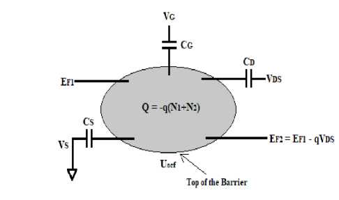
Fig.1. Two-dimensional circuit model of a CNTFET. The shaded region represents the total mobile charge. V G , V S , and V DS represent the gate bias, source bias and drain to source bias respectively.
The electron concentration at the top of the barrier at equilibrium is:
+X
N = J D ( E ) f ( E - EF ) dE (1)
-X where D(E) is the density of states at the top of the barrier and f(E-Ef) is the Fermi function at equilibrium. The function D(E) takes on non-zero values for positive values of E only and is minimum at equilibrium (E=0). The source is always grounded in this model and when a bias voltage is applied to the drain and the gate terminals, the self-consistent potential at the top of the barrier becomes Uscf. The energy states at the top of the potential barrier are now occupied by two different Fermi levels (E1 and E2). The contribution of the source and drain in filling up these energy states can be described using the relations below:
+X
N - = - J D ( E - U f ) f ( E - E f 1 ) dE (2)
-to
+x
N 2 = j J D ( E - U„ f ( E - E f 2 ) dE (3)
-to where, EF1 = EF and EF2 = (EF-qVDS). A simplified notation of the equations (2) and (3) are as follows:
+X
N- = - J D (E)f (E) dE(4)
-X
+X
N2 = - J D (E)f 2 (E) dE(5)
-X where, f1(E) = f(E+Uscf-EF1)(6)
and f2(E) = f(E+Uscf-EF2)(7)
The total charge concentration at the top of the barrier is the sum of N 1 and N 2 ( N=N 1 +N 2 ). However, in order to determine the total charge density the self-consistent potential ( Usc f ) must first be evaluated using the twodimensional Poisson equation. The charge due to applied bias is: ∆N = ( N 1 +N 2 ) -N 0 . The Laplace potential at the top of the barrier ignoring the mobile charge in the channel is given by:
UL = -q (aGVG + aDVD + asVS )
Here α G , α D , and α S are the gate, drain and source parameters respectively given by:
CCC aG = TG , aD = D and aS = TS(9)
TTT where, CT = CG+ CD+ CS. For an ideal CNTFET, αG = 1 and αD, αS = 0.
The potential due to the presence of mobile charge at the top of the barrier is:
Up = q- N N
P CT
The complete solution to the self-consistent potential ( U scf ) can be obtained by adding the contribution of the drain and the gate in pushing down the potential energy ( UL ) at the top of the barrier as well as the potential energy rise ( UP ) due to the presence of mobile charge. Therefore,
U f = UL + U p = - q ( « GVG + a D V D + « S V S ) + ^ ^ (11)
where U C = q2/C T is the charging energy. The coupled non-linear equations of (4), (5) and (11) can be solved iteratively to determine the carrier density ( N ) and the self-consistent potential ( U scf ) at the top of the barrier.
The drain current can be represented as: +^ +^
I d = J J ( E ) f . ( E ) dE - J J ( E ) f 2 ( E ) dE (12) —^ -^
where J(E) is the current density of states.
-
III. Device Structure And Input Parameters
The basic structure of the simulated SW-CNTFET having coaxial geometry is shown in Fig. 2 which has already been described in section I. In this simulation, a single wall carbon nanotube (SWCNT) acts as the channel material having a high value of doping density at the source and the drain. The following assumptions were made during the course of this investigation: contact resistance between the nanotube and metal is negligible, and transport of the charge carriers throughout the structure is ballistic (zero scatterings) in nature. In ballistic transport the mean free path of electrons is greater than the channel length; therefore the channel length does not qualify as a relevant parameter in this study.
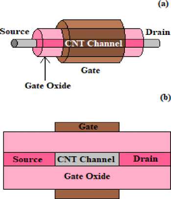
Fig.2. (a) 3-D representation of the coaxial SW-CNTFET. In practice, the source and drain ends are also buried under the gate oxide (b) simplified 2-D cross-sectional view of the SW-CNTFET coaxial structure under investigation
As discussed earlier, chirality (n, m) of the SWCNT is related to the diameter and band-gap respectively as [10]:
D=«c «Пnm ) = 0.0783V n 2 + m 2 + nm
Eg (eV) = 20- swcnt
Where γ 0 is carbon tight bond energy, α c-c is carbon bond length. In addition, the threshold voltage of a coaxial SW-CNTFET can be represented as [8]:
, _ 1 a«c - c th 3 qDswcnt
Where a is the lattice constant and q is the electronic charge. The various input parameters used in the simulation are summarised in Table 1.
Table 1. Summary of the various inputs for the simulation
|
Input Parameters |
Values |
|
CNT Chirality (n, m) |
13,0 |
|
Tight Binding Energy (eV) |
3.0 |
|
CNT Diameter (nm) |
1 |
|
Energy bandgap of CNT (eV) |
0.852 |
|
Gate oxide thickness (nm) |
2.5, 3.0, 3.5, 4.0, 4.5, 5.0 |
|
Gate oxide material |
SiO 2 |
|
Gate oxide dielectric constant |
3.9 |
|
Drain Control Parameter |
0.05 |
|
Gate Control Parameter |
0.85 |
|
Source Control Parameter |
0.0 |
|
Ambient Temperature (K) |
300 |
|
Threshold Voltage (V) |
0.3 |
|
Series Resistance (ohm) |
0 |
-
IV. Simulation Results And Discussion
Drain characteristics and transfer characteristics are the two most important curves that help us determine the performance of FETs. From the nature of these graphs, parameters such as drive current (I on ), I on /I off ratio, transconductance, amplification factor (gain), drain induced barrier lowering (DIBL) and the sub-threshold swing (SS) can be extracted. In this section, the influence of gate dielectric (SiO 2 ) thickness on various parameters mentioned above will be discussed in detail.
-
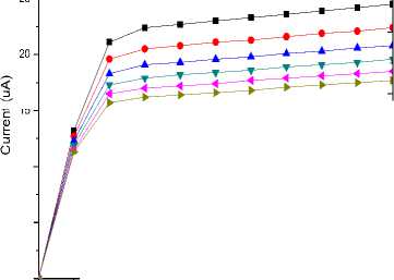
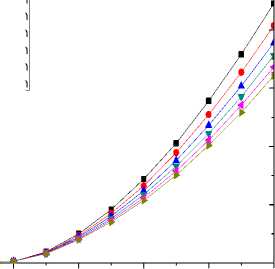
A. Drain Characteristics
Drain characteristics are the variation of drain-source current with a change in drain-source voltage. Fig. 3 shows the variation of drain current for various values of gate oxide thickness. As the thickness of the dielectric layer decreases the output saturation current increases with the effect being progressively dominant. The drain conductance can be extracted from drain characteristics and is a ratio of the change in the drain to source current to the change in the drain to source voltage for a constant gate to source voltage.
D
■ 2.5nm
• 3.0nm
—▲— 3.5nm
—▼— 4.0nm
—◄— 4.5nm
—►- 5.0nm
0.0 0.2 0.4 0.6 0.8 1.0
Drain Voltage (V)
Fig.3. Drain characteristics of the coaxial SW-CNTFET for different values of SiO2 thickness at VGS = 1V
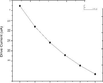
current delivering capability compared to conventional Si MOSFETs [11]. The on-current can be defined as the product of charge induced by the gate terminal and the average carrier velocity. Drive current (Ion) is the value of drain to source current at VGS = VDS = 1V, while leakage current (I off ) is the value of drain to source current at V GS = 0V and V DS = 1V. The simulation results show that the extracted value of leakage current (I off ) remains constant at 2.556x10⁻⁴µA even when the thickness of the gate oxide increases. The curves of I on clearly suggest that with the increase in dielectric thickness the gate terminal loses its control over the channel, decreasing the current carrying capability of the CNTFET (Fig. 5). A similar trend is observed in the I on /I off curve (Fig. 6) signifying that the CNTFET on-current to off-current ratio decreases with increasing insulator thickness which is undesirable. The I on and I on /I off values decrease by 27.64% for a mere 2.5nm increase in the thickness of the gate oxide.
-
B. Transfer Characteristics
2.5 3.0 3.5 4.0 4.5 5.0
Transfer characteristics are the variation of drainsource current with the change in gate-source voltage. Fig. 4 shows the alteration in the curves of the CNTFET for different values of gate oxide thickness. The nature of the curves clearly suggests that the output current increases for decreasing gate oxide thickness enhancing the current carrying capability of the FET. From the transfer characteristics, the trans-conductance of the FET can be derived, which is the ratio of the change in the drain to source current to the change in the gate to source voltage for a fixed drain to source voltage.
-•- Ion
Gate Oxide Thickness (nm)
Fig.5. On current (I on ) of the coaxial SW-CNTFET as a function of SiO 2 thickness at V GS = 1V and V DS = 1V
о
■ 2.5nm
• 3.0nm
—▲— 3.5nm
—▼— 4.0nm
-<- 4.5nm
—►- 5.0nm
0.0 0.2 0.4 0.6 0.8 1.0
Gate Voltage (V)
Fig.4. Transfer characteristics of the coaxial SW-CNTFET for different values of SiO 2 thickness at V DS = 1V
-
C. Drive Current (I on ) and I on /I off ratio
One of the several advantages CNTFET offers over bulk MOSFETs is the high current drive capability. CNTFETs typically offer over three to four times the
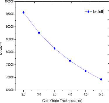
Fig.6. Ion/ Ioff ratio of the coaxial SW-CNTFET as a function of SiO2 thickness. The values of I off were determined at V GS = 0V and V DS = 1V
-
D. Trans-conductance (g m ), Output Conductance (g d ), Gain and Carrier Injection Velocity
Another important parameter that characterizes the performance of a FET is the trans-conductance. For a FET this parameter should be high and is defined as the ratio of change in the drain to source current to the change in the gate to source voltage for a constant value of drain to source voltage. The value of transconductance of a CNTFET can be determined from the transfer characteristics. The trans-conductance of a CNTFET is typically four times higher than a conventional MOSFET [11]. It is also a good measure of the gate control over the device performance. Large value of trans-conductance suggests better control of gate terminal over the charge density in the channel. Fig. 7 shows that with the decrease in SiO 2 thickness transconductance value increases indicating improved gate control over the channel. For a 2.5nm decrease in thickness of the dielectric, the trans-conductance value decreases by 26.84%.
Drain conductance is a function of the drain current in the on-state and is the ratio of change in the drain to source current to the drain to source voltage at a constant gate to source voltage. The drain current decreases with the increase in the thickness of the SiO 2 dielectric (Fig. 3). Therefore, it is obvious that the output conductance decreases with increasing thickness as evident in Fig. 8.
The gain of the CNTFET is defined as the ratio of the trans-conductance to the output conductance. As far as the results of the simulation are concerned, the output conductance of the coaxial geometry SW-CNTFET varies with the thickness of the gate dielectric layer as shown in Fig. 8. The magnitude of the decrease in transconductance in the numerator is greater than the decrease in drain conductance at the denominator. Therefore the gain shows a decreasing trend as shown in Fig. 9. Gain is a measure of the amplification provided by the CNTFET to an input signal. Therefore, high gain is a desirable criterion in CNTFETs.
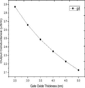
Fig.8. Drain conductance of the coaxial SW-CNTFET for different values of SiO 2 thickness
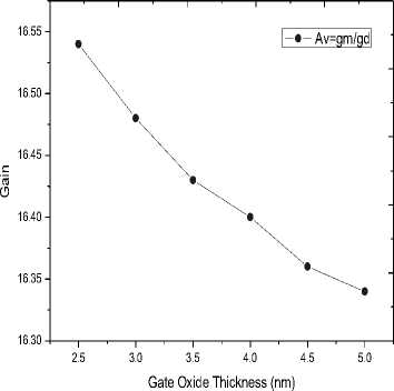
Fig.9. Gain of the coaxial SW-CNTFET for different values of SiO 2 thickness
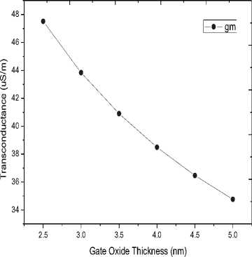
Fig.7. Trans-conductance of the coaxial SW-CNTFET for different values of SiO2 thickness
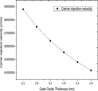
Fig.10. Carrier injection velocity of the coaxial SW-CNTFET as a function of SiO 2 thickness
Sometimes it is convenient to express the on-current of a CNTFET as the product of charge and injection velocity and is simply the average carrier velocity at the top of the barrier. The injection velocity at the highest gate bias determines the maximum on-current that a transistor can deliver [12]. Fig. 10 shows the dependence of carrier injection velocity on the dielectric thickness. The result is expected as the drain current has a direct relationship to the injection velocity. The carrier injection velocity decreases with increasing dielectric thickness, therefore the drain current follows the same trend (Fig. 3).
The results of the simulation presented thus far are in agreement with some of the studies conducted earlier on coaxial SW-CNTFETs with SiO 2 as the gate dielectric [7,8,13].
-
E. Short Channel effects (Sub-threshold Swing and DIBL)
Channel length shortening is responsible for the advent of two commonly observed phenomenons in nano-scale FETs: Sub-threshold swing and drain induced barrier lowering (DIBL). DIBL is a result of a reduction in the height of the potential barrier between the source and channel in the weak inversion regime because of the application of a high drain voltage. The barrier height of the charge carriers should ideally be controlled by a voltage applied at the gate. Because in a CNTFET the channel length is of the order of a few nanometers, the drain terminal is now closer to the gate playing its role in lowering the barrier height encountered by the charge carriers. As a consequence, the high electric field at the drain leads to an increase in the number of injected charge carriers increasing the off-current of the FET. Simulation result shows (Fig. 11) that the value of DIBL is weakly dependent on the gate oxide thickness and is lower than the theoretical limit of 100mV/V for a good CNTFET design [7].
effectiveness in reducing the drain current to zero when the gate-source voltage is less than the threshold voltage. Smaller values of sub-threshold swing are indicative of lower leakage power consumption and its ideal value is 60mV/decade [14]. Also, a low value of sub-threshold swing is indicative of a fast transition between off-state (low current) to on-state (high current). Fig. 12 shows the variation of sub-threshold swing with respect to the gate oxide thickness and increases for an increase in gate dielectric thickness. Even though the value of the subthreshold slope is best (73.61mV/decade) for the minimum gate oxide thickness of 2.5nm, it is well above the maximum permissible limit of 60mV/decade. The reason for such a high value of sub-threshold swing may possibly be attributed to the chosen value of gate control parameter (0.85).
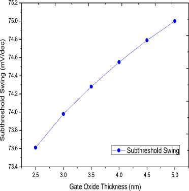
Fig.12. Sub-threshold swing of the coaxial SW-CNTFET as a function of SiO2 thickness with values greater than 60mV/decade
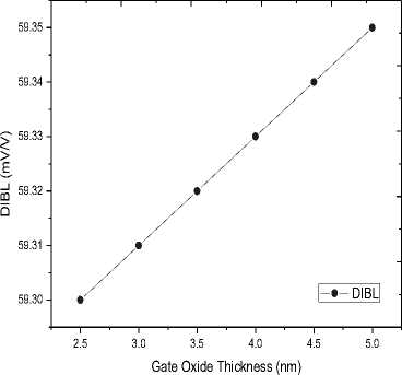
Fig.11. DIBL of the coaxial SW-CNTFET as a function of SiO2 thickness within 100mV/decade
Sub-threshold swing is the change in the gate to source voltage required to produce a unit decade change in the drain to source current. It is a measure of the
The sub-threshold swing values obtained were unsatisfactory; therefore it was decided to investigate its dependence on the gate control parameter. Because the sub-threshold swing was least for SiO 2 thickness of 2.5nm, this value was chosen for a better understanding of the sub-threshold swing variation in the CNTFET for different gate control parameters. Fig. 13 shows the dependence of sub-threshold swing variation with respect to the gate control parameter. Initially, the swing decreases for lower values of gate control coefficient reaches a minimum and then gradually increases. It is obvious from the graph that in order for the sub-threshold swing to be less the gate control parameter must not be too high or too low. A smaller value of sub-threshold swing is required for providing an adequate value of I on /I off ratio, low threshold voltage, low power operation, and faster response. In addition, from Fig. 14 it can be observed that barrier lowering due to the electric field at the drain is also reduced when the gate control parameter is equal to unity. This means that the transition from the state of pinch-off to conduction does not happen with ease when the gate control parameter is equal to one, as a result of which leakage current is reduced.
73.8
73.6
73.4
|-«- Subthreshold Swing
73.0
I 72.8
72.6
72.4
72.2
72.0
71.8
0.84 0.86 0.88 0.90 0.92 0.94 0.96 0.98 1.00
Gate control parameter
Fig.13. Sub-threshold swing of the coaxial SW-CNTFET for different values of the gate control parameter
Gate control parameter
Fig.14. DIBL of the coaxial SW-CNTFET for different values of the gate control parameter
-
V. Conclusion
In this paper, the effects of reducing SiO2 insulator thickness on the performance of a ballistic SW-CNTFET were presented in detail. Scaling down the gate insulator thickness improves the performance of SW-CNTFETs by increasing the drain current, driving current, on-current to off-current ratio, switching speed, trans-conductance, gain and the carrier injection velocity. At the same time, it does not have any significant impact on the leakage current and therefore power consumption is negligible. In addition, analysis of the short channel effects establishes that DIBL stays below its theoretical limit, while the sub- threshold swing approaches closer to its theoretical limit for a high value of gate control coefficient. Therefore, SW-CNTFET offers better scaling potential and faster response compared to conventional bulk MOSFETs along with lower power consumption. However, it must be noted that the gate oxide thickness should not be scaled down below a specific limit as it may lead to a rise of tunneling currents degrading the performance. In such cases, it is feasible to use a high-k dielectric instead of SiO2 as the gate dielectric material.
References Simulation of a ballistic SW-CNTFET with coaxial geometry: numerical approach to determine the impact of gate oxide thickness on the performance
- H. Liu, A.T. Neal, P.D. Ye, “Channel length scaling of MoS2 MOSFETs”, ACS Nano, vol. 6, no. 10, pp. 8563–8569, 2012.
- D.A. Antoniadis, I. Aberg, C.N. Chléirigh, et al. “Continuous MOSFET performance increase with device scaling: the role of strain and channel material innovations”, IBM J. Res. Dev., vol. 50, no. 4, pp. 363–376, 2006.
- J.W.G. Wilder, L.C. Venema, A.G. Rinzler, R.E. Smalley, C. Dekker, “Electronic structure of atomically resolved carbon nanotubes”, Nature, vol. 391, pp. 59-62, 1998.
- K. Boucart, A.M. Ionescu, “Double-gate tunnel FET with high-k gate dielectric”, IEEE Trans. Electron Devices, vol. 54, no. 7, pp. 1725–1733, 2007.
- J. Robertson, “High dielectric constant gate oxides for metal oxide Si transistors”, Rep. Prog. Phys., vol. 69, no. 2, pp. 327-396, 2005.
- S. Thompson, “MOS scaling: transistor challenges for the 21st century”, Intel Technol. J., vol. 398, pp. 1–9, 1998.
- D. Dass, R. Prasher, R. Vaid, “Impact of Scaling Gate Insulator Thickness on the Performance of Carbon Nanotube Field Effect Transistors (CNTFETs)”, Journal of Nano- and Electronic Physics, vol. 5, no. 2, pp. 1-6, 2013.
- J.K. Saha, N. Chakma, M. Hasan, “Impact of channel length, gate insulator thickness, gate insulator material, and temperature on the performance of nanoscale FETs”, Journal of Computational Electronics, 2018.
- K. Natori, “Ballistic metal‐oxide‐semiconductor field effect transistor”, J. Appl. Phys., vol. 76, no. 8, 1994.
- F. Leonard, “Physics of Carbon Nanotube Devices”, William Andrew Inc.: USA, 2009.
- R. Sahoo, R. R. Mishra, “Simulations of Carbon Nanotube Field Effect Transistors”, International Journal of Electronic Engineering Research, vol. 1, no. 2, pp. 117–125, 2009.
- J. Guo, M. Lundstrom, S. Datta, “Performance projections for ballistic carbon nanotube field-effect transistors”, Applied Physics Letters, vol. 80, no. 17, 2002.
- D. Dass and R. Vaid, “Impact of SWCNT Band Gaps on the Performance of a Ballistic Carbon Nanotube Field Effect Transistors (CNTFETs)”, Journal of Nano- and Electronic Physics, vol. 9, no. 4, pp. 1-5, 2017.
- Q. Chen, B. Agrawal, J. Meindl, “A comprehensive analytical sub-threshold swing (S) model for double-gate MOSFETs”, IEEE Trans. Electron Devices, vol. 49, no. 6, pp. 1086–1090, 2002.
