Simulation of a discharge device for the spacecraft power supply system

Author: Krasheninnikova O.V., Lobanov D.K.
Journal: Siberian Aerospace Journal @vestnik-sibsau-en
Section: Aviation and spacecraft engineering
Article in issue: 1 vol.27, 2026.
Free access
The use of spacecraft power supply stands for educational purposes is of great relevance in the modern world. The stands help students of technical specialties to better understand the principles of electrical circuits, electronics and electrical engineering, increasing the visibility of their work. They allow you to conduct practical exercises, demonstrating various types of structures, circuits and devices. The use of power supply stands also helps to stimulate the interest of technical students in science, improves their understanding of theoretical concepts and the current level of technology development, and helps develop practical problem-solving skills. To create the stand, it will be necessary to develop all the elements of the spacecraft's power supply system: a load device; a solar battery simulator; a battery simulator; a charger; a discharge device; a voltage stabilizer; control equipment. In this paper, a simulation model of the discharge device layout of the spacecraft power supply system was developed and described, allowing computational experiments to study the static and dynamic properties, stability and quality of transients. Computational experiments have been performed, the result of which is presented in the form of graphs confirming. the correctness of static and dynamic calculations of the discharge device layout. Computational experiments have been performed, the result of which is presented in the form of graphs illustrating the possibilities of a simulation model of a discharge device.
Discharge device, stand, power supply system, spacecraft, simulation
Short address: https://sciup.org/148333273
IDR: 148333273 | UDC: 629.4.051.2 | DOI: 10.31772/2712-8970-2026-27-1-108-122
Text of the scientific article Simulation of a discharge device for the spacecraft power supply system
One of the main systems of a spacecraft is the power supply system [1; 2] – this is an interconnected set of equipment used for the production and conversion, transmission, accumulation, distribution and consumption of electrical energy. The service life of the power supply system determines the active life of the spacecraft. One of the important aspects to consider when designing such systems are the standards regarding on-board network types [3] and voltage levels. Currently, two main power supply standards are accepted in the space industry: 27 and 100 V. Typically 27V is used to power utility systems and low-power consumers. Switching to a 100V bus for high-power consumers allows to reduce the current required to transmit the same power and to use a smaller cable cross-section, resulting in savings of materials and reduction in the weight of a system.
Most spacecraft use solar panels as their primary energy source [4; 5], but the position of the spacecraft relative to the Sun varies, which can affect the amount of solar energy they receive. For example, when passing through the planet's shadow, solar panels may receive less energy, which necessitates the use of a battery in the shadow portion of the orbit.
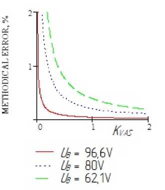
The battery contains battery cells connected in series to increase the overall voltage. The research considers the battery operating in the voltage range from 62.1 to 96.6 V, while the consumer bus voltage is 100 V, which determines the need to use a step-up converter in the discharge device.
To stabilize the output voltage of the discharge device at the required level, it is necessary to perform the following:
-
– static analysis and synthesis, including the selection of a structural diagram, calculation of its ratings, calculation of the error in voltage stabilization in the steady-state mode;
-
– dynamic analysis and synthesis, based on the results determining the parameters of the corrective device, ensuring the required stability reserves and quality parameters of transient processes;
-
– development of a simulation model of a discharge device layout;
-
– computational experiments with a simulation model, confirming the correctness of previously performed calculations;
-
– adjustment of calculations if necessary.
The MathCAD 12 computer algebra package [6] was chosen as the program for mathematical calculations. It is related to automated design systems and allows to to perform the calculations with sufficient accuracy, deal with equations and systems of equations, plot graphs, and create interactive documents.
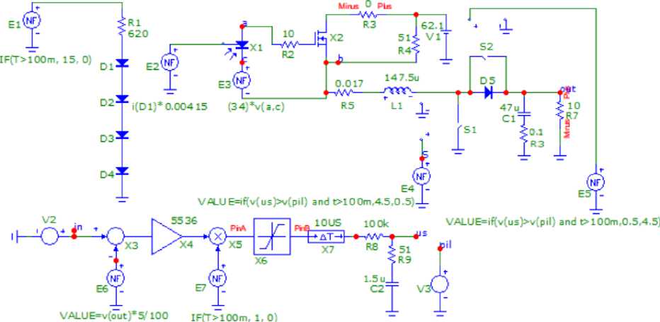
To analyze the parameters and test the operation of the discharge device with the element ratings selected based on the calculation results, the Micro-Cap 12 circuit simulation package is selected, as it obtains the following features:
-
– easy edition of SPICE models [7; 8] of components and their parameters;
-
– simulation of analog and digital electrical circuits;
-
– fairly wide range of tools for analyzing electrical circuits;
-
– multivariate analysis of circuits (analysis of transient processes, frequency analysis, analysis of transfer functions with varying parameters).
Using the developed discharge device model as part of a model of a spacecraft power supply system in the educational process will allow students to visually study the principles of constructing spacecraft power supply systems, the processes occurring in them, and telemetry information.
Static calculation of the discharge device
When developing the layout of the discharge device, a static analysis was carried out; it resulted in determining the block diagram presented in Fig. 1.
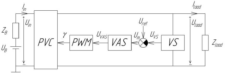
Рис. 1. Структурная схема разрядного устройства:
УС – усилитель напряжения; ИПН – импульсный преобразователь напряжения; ДН – датчик напряжения; ШИМ – широтно-импульсный модулятор; γ – коэффициент заполнения; U УС – напряжение усилителя-сумматора; U АБ – напряжение аккумуляторной батареи; Z АБ – сопротивление аккумуляторной батареи; U ВХ – входное напряжение преобразователя; I ВХ – входной ток преобразователя;
U Д Н – напряжение датчика напряжения; Uε – напряжение рассогласований; U ОП – опорное напряжение;
U Н, I Н и Z Н – напряжение, ток и сопротивление нагрузки
-
Fig. 1. Block diagram of the discharge device:
VAS – voltage amplifier-summer; PVC – pulse voltage converter; VS – voltage sensor;
PWM – pulse width modulator; γ – duty cycle; UVAS – voltage amplifier-summer; UB – battery voltage; Z B – battery impedance; Uin – input voltage of the converter; Iin – input current of the converter; U VS – voltage of the voltage sensor;
U m – mismatch voltage; U re f – reference voltage; Uload , Iload and Zload – voltage, current and load resistance
The discharge device has got the following technical requirements:
– voltage change ranges from 62.1 to 96.6 V;
-
– current ranges from 1 to 10 A;
-
– the amplitude of output voltage pulsations is no more than 1 V;
-
– output voltage stabilization error is no more than 1 %;
-
– ensured voltage stabilization is at 100 V;
-
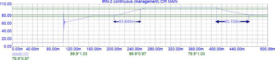
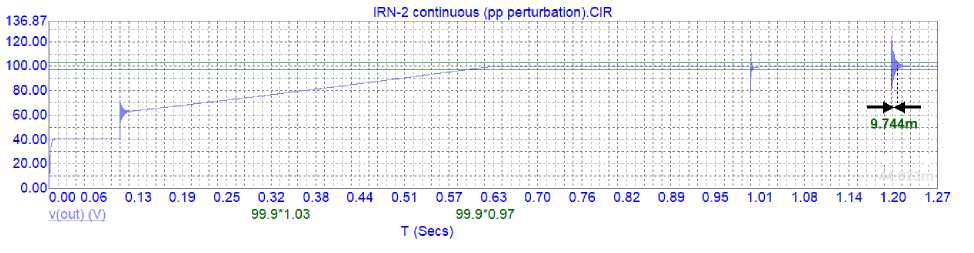
– adjusting time for the output voltage of the battery cell is no more than 1300 ms;
-
– overshoot of the output voltage of the battery cell is no more than 5 %.
To ensure voltage stabilization mode, the basis of the discharge device is an output voltage stabilizer. The output voltage stabilizer must contain a controlled pulse converter and a control system. The controlled pulse converter [9; 10] can be made in the form of a step-up pulse converter, the circuit of which is shown in Fig. 2.
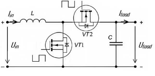
Рис. 2. Схема повышающего импульсного преобразователя
-
Fig. 2. Diagram of the boost pulse converter
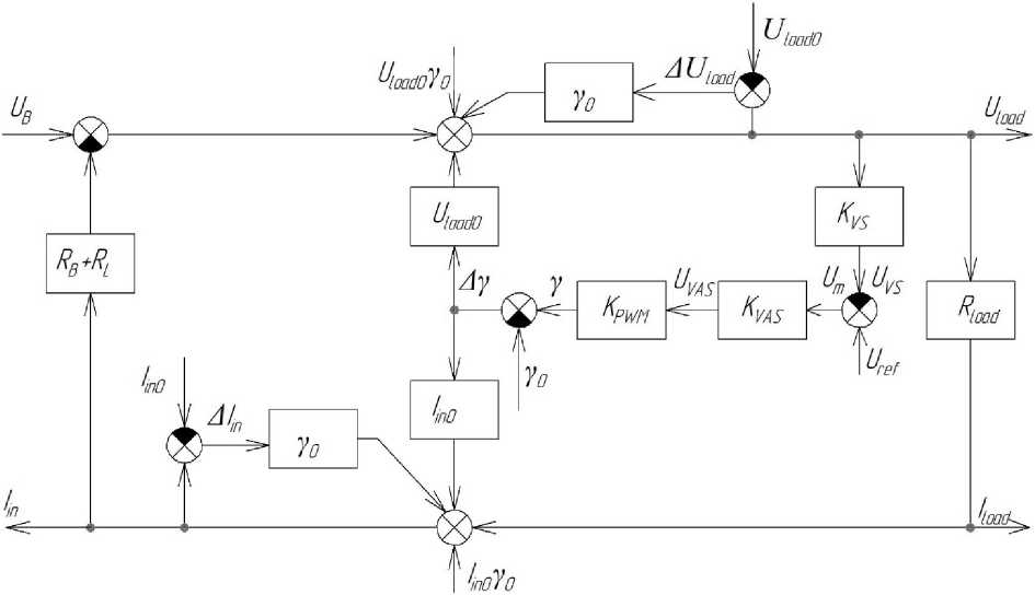
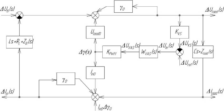
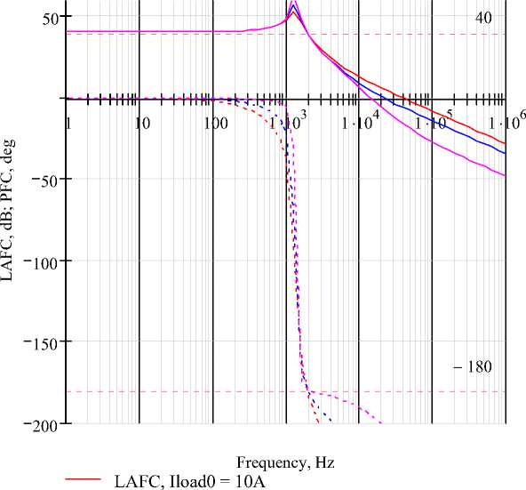
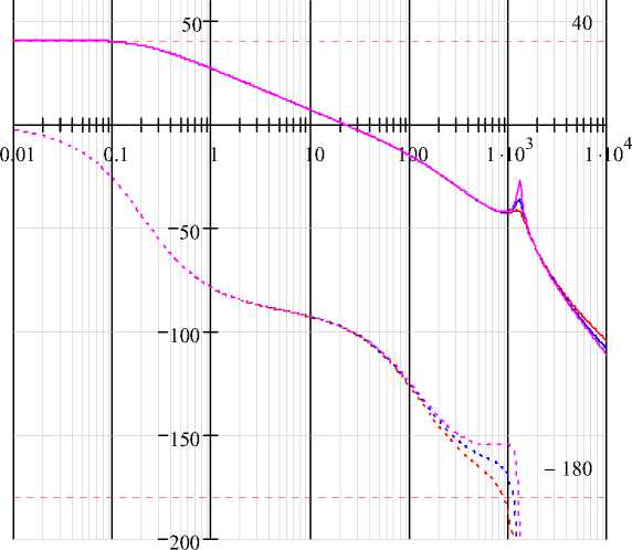
There is a mathematical description illustrating the currents and voltages flowing in the discharge device, presented in the form of systems of equations for static (1) and dynamic small-signal (2) modes; functional diagrams are developed (Fig. 3, 4), the construction of which provided the most visual representation of the sequence of processes occurring in the device; a calculation of the stabilization error of the output voltage of the step-up pulse voltage converter is performed.
Uladd = Uln - R L lm + Ul0 a d 0 Y 0 + Uш 0 A 7 + 7o A Ulo a d ,
I in = I ln0 Y 0 + I ln0 A Y + Y 0 A Iin + I load ,
m = U b — R b Im , , (1)
Um = ( Uref - Uload K VS ) K VAS ,
, Y = Um K PWM ,
RL – resistance of the winding; Uload 0 – value of the load voltage at the linearization point.; γ0 – value of the fill factor at the linearization point.; Δγ – increment of the fill factor value; Δ Uload – increment of the load voltage value; I in 0 – value of the input current at the linearization point.; Δ I in – increment of the input current value; RB – active component of the battery resistance; KVS – voltage sensor coefficient; KVAS – static transmission coefficient of the VAS; KPWM – pulse width modulator coefficient.
A Uload ( s ) = A Un ( s ) - ( RL + Ls ) AIin ( s ) + Uload0 AY( s ) + Yo A Uload ( s ),
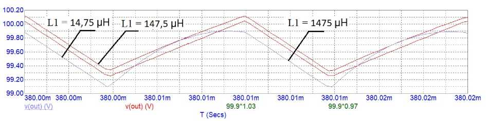
|
Inductance (µH) |
Pulsation amplitude (V) |
|
14,75 |
0,451 |
|
147,5 |
0,453 |
|
1475 |
0,454 |
Fig. 11 and Table 1 allows to conclude that in a step-up converter at a switching frequency f K = 154170.8 Hz, the amplitude of the output voltage pulsations remains practically unchanged when the inductance changes.
As Fig. 12 illustrates, when changing the capacity of the output capacitor, the output voltage pulsations in transient disturbance processes will change.
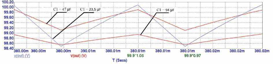
Рис. 12. Пульсации выходного напряжения при изменении емкости выходного конденсатора в диапазоне от 23,5 до 94 мкФ
Fig. 12. Pulsations of the output voltage when changing the capacitance of the output capacitor in the range from 23,5 to 94 μF
Table 2 shows the dependence of the output voltage pulsation amplitude on the value of the capacitance of the output capacitor of the discharge device.
Table 2
Dependence of the pulsation amplitude on the value of the output capacitor capacitance
|
Capacitance (μF) |
Pulsation amplitude (V) |
|
23,5 |
0,784 |
|
47 |
0,440 |
|
94 |
0,187 |
Due to Table 2, we can conclude that the larger the value of the output capacitor, the smaller the pulsation amplitude.
We are constructing the impedance-frequency characteristic (IFC) in Fig. 13 for different values of the inductance of the choke L1.
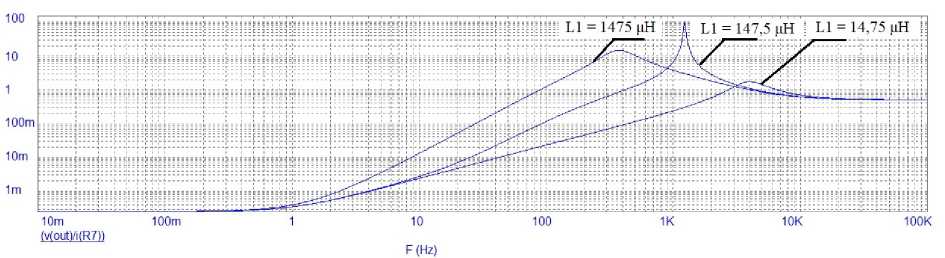
Рис. 13. Графики ИЧХ при изменении индуктивности в диапазоне от 14,75 до 1475 мкГн
Fig. 13. Graphs of the impedance-frequency characteristic (IFC) with a change in inductance in the range from 14,75 to 1475 μH
Based on Fig. 13, we can conclude that the lower the inductance of the choke, the higher the resonant surge frequency.
Table 3 presents the dependence of the resonant emission frequency to IFC on the inductance of the discharge device choke.
Table 3
|
Inductance (µH) |
Frequency (kHz) |
|
14,75 |
3,896 |
|
147,5 |
1,234 |
|
1475 |
0,370 |
Dependence of the resonant emission frequency on the inductance of the discharge device choke
We are constructing the impedance-frequency characteristic (IFC) in Fig. 14 for different values of the output capacitor C1.
Рис. 14. Графики ИЧХ при изменении емкости выходного конденсатора в диапазоне от 4,7 до 470 мкФ
Fig. 14. IFC graphs with a change in the capacity of the output capacitor in the range from 4,7 to 470 μF
Fig. 14 allows to conclude that the less capacity of the output capacitor, the higher the resonant surge frequency.
Table 4 presents the dependence of the resonant emission frequency to IFC on the capacity of the output capacitor of the discharge device.
Table 4
Dependence of the resonant emission frequency on the value of the capacitance of output capacitor
|
Capacity (μF) |
Frequency (kHz) |
|
4,7 |
3,842 |
|
47 |
1,230 |
|
470 |
0,418 |
We construct the IFC in Fig. 15 for different values of the gain factor K VAS .
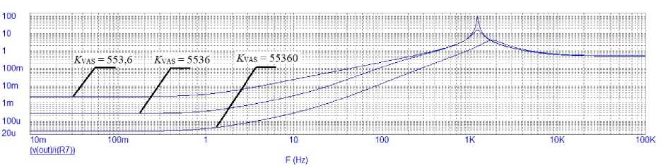
Рис. 15. Графики ИЧХ при изменении коэффициента усиления K УС в диапазоне от 553,6 до 55360
Fig. 15. IFC graphs with a change in the gain factor K VAS in the range from 553,6 to 55360
Fig. 15 make it possible to conclude that the higher the gain factor K VAS, the smaller the active component of the IFC.
Table 5 shows the dependence of the change in the value of the active component of the IFC on the coefficient of the amplifier-summer of the discharge device.
Table 5
Dependence of the change in the active component of the IFC on the coefficient of the amplifier-summer
|
K VAS |
Active component of the IFC (mOhm) |
|
553,6 |
2,397 |
|
5536 |
0,255 |
|
55360 |
0,025 |
Conclusion
The developed simulation model of the discharge device allows to verify the correctness of static and dynamic calculations by constructing graphs that determine the cutoff frequency, phase margin, and regulation time. The discharge device model also permits the computational experiments to study the static and dynamic properties, stability and quality of transient processes of the discharge device.
The discharge device model illustrates the capabilities of the simulation model and makes it possible to evaluate the impact of changes in the parameters of key circuit elements: choke inductance, capacitor capacitance, and load on transient processes and IFC.
