Single Chip Embedded System Solution: Efficient Resource Utilization by Interfacing LCD through Softcore Processor in Xilinx FPGA

Автор: Shiraz Afzal, Farrukh hafeez, Muhammad Ovais Akhter
Журнал: International Journal of Information Engineering and Electronic Business(IJIEEB) @ijieeb
Статья в выпуске: 6 vol.7, 2015 года.
Бесплатный доступ
This paper presents a customized application in term of LCD interfacing through soft-core microcontroller by implementing its control circuitry in FPGA. Therefore optimum efficiency is achieved. This provide the single chip solution by replacing conventional model which contain separate microcontroller circuit, therefore the efficient resource utilization of FPGA is made, day by day as an increase in the complexity of Embedded system design thus gives many advantages over conventional designed processors such as platform independence, less cost, flexibility and greater immunity to obsolescence.
FPGA, LCD interfacing, soft-core microcontroller e.t.c
Короткий адрес: https://sciup.org/15013377
IDR: 15013377
Текст научной статьи Single Chip Embedded System Solution: Efficient Resource Utilization by Interfacing LCD through Softcore Processor in Xilinx FPGA
Published Online November 2015 in MECS DOI: 10.5815/ijieeb.2015.06.04
A microcontroller is the major part of any embedded system that uses both hardware and software components to perform specific application. As embedded systems play a vital role in our everyday life also exist in profusion in our modern civilization and can be found in places such as in our vehicle, in health field, in industries and in amusement electronics to name just a few [1].
As an increase in complexity of embedded system. It became very difficult to design each hardware component because of the cost and become impractical approach therefore the emergence of Soft core microcontroller solve this problem in which a designer can easily build their design and verify that.
Here in this manuscript an important hardware element that relates to the embedded system which is LCD interfacing through soft-core controller is being controlled through Xilinx picoblaze controller as shown in Fig. 1.
The material of the manuscript is arranged as follow in section II explains the survey of softcore processors. Section III we describe the software used for HDL Language. Section IV describe the FPGA implementation which involves subsections as follow: Sub-section “a” describe the Pico-blaze Microcontroller Overview. Subsection “b” describes the VHDL component and design
-
II. Review of Available Soft-Core Processors
This segment provide a list of available softcore processor specified by the both open source communities and commercial vendorsare provided
-
A. Open Resource Softcores
An open source community provides various cores freely available as given in [2]. These types of softcores are not only used for research purpose but also for the development of embedded systems [3], an example of such type of core used in academia for research purpose is UT Nios [4]. Another listof cores which is not only used forthe ASICs but can be also used for modeling and synthesize of FPGA is OpenSPARC [5]. Further LEON [6], LEON2 [6], LEON3 [5], Open RISC 1200 [2] and sun microsystem as provides theirown core are also available as open source soft cores. Details of which are available in [3].
-
B. Commercial Available Softcores:The major softcore controller includes Microblaze, Picoblaze by Xilinx, Nios II by Altera and Xtensa by Tensilica [3].
Microblaze and Picoblaze: This 32bit and 8bit softcore processor are incorporated by Xilinx for both Spartan and Virtex series, one of the leading vendor of FPGA. Microblaze is one of the demanding and mostly used softcore processor. It uses a Harvard RISC architecture, having 32 bit instruction set, and two level of interrupts and can operate up to 200MHz on Virtex 4 FPGAwhile Picoblaze is a compact 8 bit softcore controller can be useful for simple data processing application because of its miniature element and cost effective features [3].
Nios II by Altera: is a general purpose softcore processor that uses Harvard RISC architecture, 32 bit instruction set. It comes in three versions fast core, standard and economy further each core varies in performance and dimension depending on the chosen feature
-
III. Tool Used
Xilinx 8.2i is used for the programming and configuring of FPGA, It give user friendly environment and can also provide flexibility in terms of by either implementing the logic using basic logical operator or with schematic diagram using schematic editor implementation.
Here in this task the LCD is programmed using VHDL language, further for picoblaze softcore processor KCPSM3 assembler is used. DOSBOX 0.74 is used for picoblaze psm file simulation.
-
IV. Implementation
The work is carried out in the following segments:
A.Picoblaze Processor overview.
-
B. VHDL Components and design processes.
C.Picoblaze instruction set.
-
D. LCD display overview.
-
A. Picoblaze Overview
Fig. 2 shows the block diagram of picoblaze microcontroller, the significance of using picoblaze is of its small size, having RISC architecture and less FPGA slice available only 96 slices. It is given as a free, sourcelevel VHDL file with royalty-free re-use within Xilinx
FPGAs [8].
There main feature includes 64 bytes of internal memory, 256 input and output ports available, 16 byte wide general purpose register.
-
B. VHDL Component and Design Processes
VHDL components used by the picoblaze controller is shown in Fig. 3.They are mainly divide into two components that is block memory ROM and KCPSM3, KCPSM3 component provide the registers, Arithmetic logic unit etc.
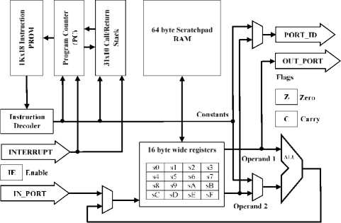
Fig.2. Block diagram of Picoblaze microcontroller
-
C. PicoblazeInstruction Set: The instructions mainly used by the picoblaze microcontroller is shown in table [3 manualref.].
Fig.3. VHDL components used by the picoblaze controller
Table 1. VHDL Instructions with Description
|
Instruction |
Description |
|
ADD aX, mm |
Add register aX with literal mm. |
|
ADD aX, bY |
Add register aX with register bY. |
|
ADDCY aX, mm |
Add register aX with literal mm with CARRY bit. |
|
ADDCY aX, bY |
Add register aX with register bY with CARRY bit. |
|
AND aX, mm |
Bitwise AND register aX with literal mm. |
|
AND aX, bY |
Bitwise AND register aX with register bY. |
|
CALL zzz |
Unconditionally call subroutine at zzz. |
|
CALL C, zzz |
If CARRY flag set, call subroutine at zzz. |
|
CALL NC, zzz |
If CARRY flag not set, call subroutine at zzz. |
|
CALL NZ, zzz |
If ZERO flag not set, call subroutine at zzz. |
|
CALL Z, zzz |
If ZERO flag set, call subroutine at zzz. |
|
COMPARE aX, mm |
Compare register aX with literal mm Set CARRY and ZERO flags asappropriate. Registers are unaffected. |
|
COMPARE aX, bY |
Compare register aX with register bY. Set CARRY and ZERO flags as appropriate. Registers are unaffected |
|
DISABLE INTERRUPT |
Disable interrupts. |
|
ENABLE INTERRUPT |
Enable interrupts. |
|
FETCH aX, bY |
Read scratchpad RAM location pointed to by register bY into register aX. |
|
FETCH aX, ss |
Read scratchpad RAM location ss into register aX. |
|
INPUT aX, bY |
Read value on input port pointed to by register bY into register aX. |
|
INPUT aX, pp |
Read value on input port pp into register aX. |
|
JUMP zzz |
Unconditionally jump to zzz. |
|
JUMP C, zzz |
If CARRY flag set, jump to aa. |
|
JUMP NC, zzz |
If CARRY flag not set, jump to aa. |
|
JUMP NZ, zzz |
If ZERO flag not set, jump to aa. |
|
JUMP Z, zzz |
If ZERO flag set, jump to aa. |
|
LOAD aX, mm |
Load register aX with literal mm. |
|
LOAD aX, bY |
Load register aX with register bY. |
|
OR aX, mm |
Bitwise OR register aX with literal mm. |
|
XOR aX, bY |
Bitwise XOR register aX with register bY. |
|
XOR aX, mm |
Bitwise XOR register aX with literal mm. |
|
TEST aX, bY |
Test bits in register aX against register bY. Update CARRY and ZEROflags. Registers are unaffected. |
|
TEST aX, mm |
Test bits in register aX against literal mm. Update CARRY and ZEROflags. Registers are unaffected. |
|
SUBCY aX, bY |
Subtract register bY from register aX with CARRY (borrow). |
|
SUBCY aX, mm |
Subtract literal mm from literal aX with CARRY (borrow). |
|
SUB aX, bY |
Subtract register bY from register aX. |
|
SUB aX, mm |
Subtract literal mm from literal aX. |
|
STORE aX, ss |
Write register aX to scratchpad RAM location ss. |
|
STORE aX, bY |
Write register aX to scratchpad RAM location pointed to by register bY. |
|
SRX aX |
Shift register aX right. Bit aX[7] is unaffected. |
|
SRA aX |
Shift register aX right through all bits, including CARRY. |
|
SR1 aX |
Shift register aX right, one fill. |
|
SR0 aX |
Shift register aX right, zero fill. |
|
SLX aX |
Shift register aX left. Bit aX[0] is unaffected. |
|
SLA aX |
Shift register aX left through all bits, including CARRY. |
|
SL1 aX |
Shift register aX left, one fill. |
|
SL0 aX |
Shift register aX left, zero fill. |
|
RR aX |
Rotate aX register right. |
|
RL aX |
Rotate aX register left. |
|
RETURNI ENABLE |
Return from interrupt service routine. Re-enable interrupt. |
|
RETURNI DISABLE |
Return from interrupt service routine. Interrupt remains disabled. |
|
RETURN Z |
If ZERO flag set, return from subroutine. |
|
RETURN NZ |
If ZERO flag not set, return from subroutine. |
|
RETURN NC |
If CARRY flag not set, return from subroutine |
|
RETURN C |
If CARRY flag set, return from subroutine. |
|
RETURN |
Return unconditionally from subroutine. |
|
OUTPUT aX, pp |
Write register aX to output port location pp. |
D. LCD Display
Spartan 3E uses 2×16 display consist of 2lines of 16 character each. LCD is controlled by FPGA through an interface and also connected with Intel Startaflash whose function is to give full write/read access to LCD as shown in the Fig. 4.
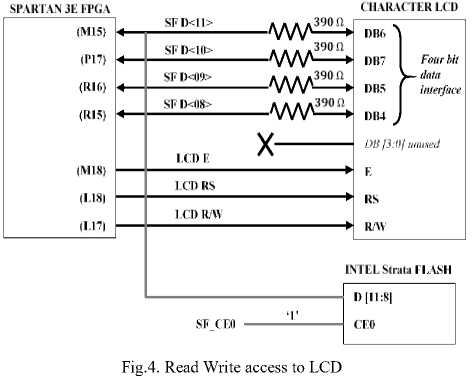
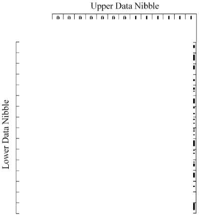
Fig.6. Font Bitmap Characters for LCD Display
|
0 |
0 |
1) |
0 |
1) |
0 |
0 |
1 |
1 |
1 |
1 |
1 |
1 |
||
|
0 |
0 |
0 |
1 |
1 |
1 |
1 |
0 |
1) |
1 |
1 |
1 |
1 |
||
|
0 |
1 |
1 |
0 |
1) |
1 |
1 |
1 |
1 |
0 |
0 |
1 |
1 |
||
|
0 |
0 |
1 |
1) |
1 |
1) |
1 |
0 |
1 |
0 |
1 |
0 |
1 |
||
|
xxxx |
0ШЮ |
0 |
s |
p |
F |
— |
у |
сс |
р |
|||||
|
xxxx |
01)01 |
I |
1 |
A |
Q |
-a |
*=1 |
D |
7 |
¥ |
-в |
а |
||
|
xxxx |
0010 |
II |
5 |
В |
В |
Б |
г |
-l" |
А |
й |
||||
|
xxxx |
0011 |
J |
# |
3 |
C |
S |
C- |
г |
-1 |
T" |
F |
£. |
-:-^ |
|
|
xxxx |
OHIO |
о |
■4 |
□ |
T |
cl |
t, |
X |
ь |
fr |
А |
П |
||
|
xxxx |
0101 |
5 |
E |
u |
e |
u |
■ |
?r |
д |
G |
Cl |
|||
|
xxxx |
0110 |
Sc |
6 |
F |
и |
Г |
=3 |
л |
3 |
А |
г |
|||
|
xxxx |
0111 |
7 |
G |
и |
9 |
w |
=F |
7? |
А |
7Г |
||||
|
xxxx |
1000 |
c |
S |
H |
м |
К |
X |
и" |
О |
Т |
и |
-.Г |
X |
|
|
xxxx |
1001 |
> |
9 |
I |
V |
i |
у |
■±i |
'Г |
J |
1Ь |
Ч |
||
|
xxxx |
1010 |
* |
J" |
z |
J |
52 |
ZE |
п |
ih |
1/ |
i |
¥ |
||
|
xxxx |
1011 |
4- |
к |
E |
k |
{ |
7t |
у |
t |
□ |
т; |
|||
|
xxxx |
1100 |
у |
< |
L |
¥ |
1 |
1 |
■h- |
z^ |
■31 |
А |
Ф |
гч |
|
|
xxxx |
1101 |
— |
= |
Г1 |
J |
Pl |
} |
ZL |
77 |
t |
ч- |
|||
|
xxxx |
1110 |
■ |
> |
N |
ri |
-* |
3 |
te |
- |
и |
||||
|
xxxx |
1111 |
v |
О |
— |
о |
■У |
V |
7? |
п |
о |
■ |
|||
While the LCD display data ram locations shows in Fig. 5, only 32 characters can be displayed at a time.
Block RAM initialization templates for a design flows
Character Display Address Г «displayed Address
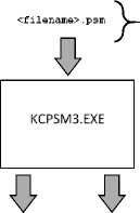
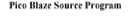
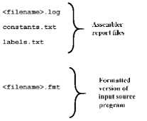
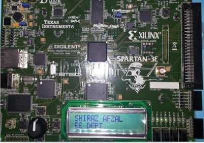
Assembler intermediate processing files (possibly useful for 0(1 01 02 03 04 05 06 07 08 09 tA 0B ОС 0D 0B OF я 41 42 43 44 45 46 47 48 49 4A 4B 4C 4B 4B 4F I 2 3 4 5 6 7 8 9 10 11 12 13 14 15 16 17.,.40 Fig.5. LCD Display The commands to controlled LCD is sum up in the Table 2. formatted la iuilhike a Block RAM tor a variety Fig.7. KCPSM3 Assembler Table 2. Commands Controlled LCD Function p J к а1 Upper Nibble Lower Nibble Q 2 Q а 2 Q 2 а 2 Q 2 а 2 Q Clear Display 0 I) 0 0 0 0 0 0 0 I Return Cursor Home 0 0 0 0 0 0 0 0 1 Enter Mode set 0 0 0 0 0 0 0 i ID 1 s Display On/OfT 0 0 1) 0 0 0 1 D C в cursor and Display Shift 0 0 1) 0 0 1 sc RI. Function Set 0 0 0 0 1 0 1 0 Set CGRAM Address 0 1) I) I 45 44 43 42 41 40 Set DDRAM Address 0 0 1 A6 45 44 43 42 41 40 Read Busy Flag and Address 0 1 BF A6 45 44 43 42 41 40 Wrile Data to ( GRAM or DDRAM 1 1) D7 D6 D5 D4 D3 D2 D1 DO Read Data from CGRAM or DDRAM 1 1 D7 D6 D5 D4 D3 1)2 D1 DO The font bitmap for the characters stored in character generator ROM, It contains the Japanese kana characters and ASCII characters as shown in the Fig. 6. In this assignment a KCPSM3 assembler is used which translates the input psm file and also three block RAM initialization templates and produces the output as shown in Fig. 7. V. Simulation Results Fig. 9 shows the simulation result by displaying the name on the 2 line 16 character LCD using softcore picoblaze controller of Xilinx Spartan 3E FPGA. Fig.9. Result display on LCD

Список литературы Single Chip Embedded System Solution: Efficient Resource Utilization by Interfacing LCD through Softcore Processor in Xilinx FPGA
- Mishra, P. and Dutt, N., "Architectural description languages for programmableembedded system",IEE Proceedings of computer and digital technique, May 2005, pp. 285-297.
- Opencores.org Website, www.opencores.org, June 2006.
- Jason GT. Tong, Ian D. L Anderson and Muhammad A. S. Khalid, "Softcore processors for embedded system", IEEE Microelectronics International Conference, Dec 2006, pp. 170-173.
- UT Nios Homepage, www.eecg.toronto.edu/Uplavec/utnios.html, June, 2006.
- Open SPARC Website, www.opensparc.org, June 2006.
- "GRLIB IP Core User's Manual", Gaisler Research, February 2006.
- "LEON2 Processor User's Manual XST Edition", Gaisler Research, July 2005.
- PicoBlaze 8-bit Embedded Microcontroller User Guide, Online: http://www.xilinx.com/support/documentation/ip_documentation/ug129.pdf, accessed 3 Dec 2012.
