Specificity of defect formation in detectors based on cadmium telluride under pulsed thermal influence

Author: Mozzherin A.V., Paklin N.N., Loginov Yu.Yu.
Journal: Siberian Aerospace Journal @vestnik-sibsau-en
Section: Technological processes and material science
Article in issue: 3 vol.25, 2024.
Free access
Active development of science-intensive technologies in the aerospace industry requires consideration of the operation of devices and instruments under extreme conditions; it is important to study the degradation of materials during rapid heating and cooling. On the basis of the theoretical and experimental work performed, the authors of the paper consider the degradation of cadmium telluride detectors caused by the development and evolution of a network of point defects resulting from pulsed exposure with a heat dose of about 1,000º С for no more than 10 s, simulating an extreme situation of a short circuit near the detector or direct heating by light pulses. The study showed that the crystalline material quickly degrades under such extreme conditions due to the rapid evolution of the defect network. The phenomenological model of the formation and distribution of defects during short-term exposure of the detector to thermal radiation has been improved. Electron microscopic studies of samples exposed to pulsed infrared radiation showed the development of a dense defect network, vacancy and interstitial defects, their clusters and other damage in all samples.
Cadmium telluride, point defects, defect clusters, thermal defect formation
Short address: https://sciup.org/148329751
IDR: 148329751 | UDC: 614.84 | DOI: 10.31772/2712-8970-2024-25-3-384-390
Text of the scientific article Specificity of defect formation in detectors based on cadmium telluride under pulsed thermal influence
The aerospace industry, which is actively developing at present, increasingly faces non-standard tasks arising as a result of the operation of devices and equipment in extreme conditions under pulsed thermal and radiation effects or emergency situations, such as fires and explosions.
Detectors based on cadmium telluride are used as devices for recording pulses of a certain type of radiation [1; 2]. Under certain circumstances, the temperature in the equipment operating area can reach an enormous value, leading to the degradation of materials and, subsequently, the failure of devices and equipment. It is well known that the effect of infrared radiation on a crystalline material leads to the formation and development of a defective structure in it, the evolution of which entails a change in the physicochemical properties. Point defects under the influence of external factors can form clusters that form volumetric defects, which, on the one hand, can lead to the rapid destruction of the material, but on the other hand, up to a certain point, allows it to withstand this destruction. Individual issues of formation and evolution of defects in semiconductors were described earlier in [3–7].
Let us consider an extreme situation when a detector based on cadmium telluride (CdTe) is exposed to extremely high temperatures of 1.000 ºС. Since the melting point of CdTe is 1.092 ºС and the previously mentioned thermal effect is critical for this semiconductor, the limit of its stability in solidcrystal and thin-film samples is of interest.
The aim of the study is to better understand the defect formation processes leading to the degradation of cadmium telluride under short-term pulsed thermal effect with heating up to 1.000 ºС.
Materials, methods and practical results
The object of the study was cadmium telluride, a direct-gap semiconductor of the AIIBVI group, one of the promising and actively used materials in microelectronics. The main properties of the material under study are presented in Table 1.
Some physicochemical properties of cadmium telluride [5; 8; 9]
Table 1
|
Density |
5.85 g/cm3 |
|
Melting temperature |
1.092 ºС |
|
Solubility in water and other solvents |
insoluble |
|
Crystalline structure |
cubic, sphalerite (zinc blende) |
|
Lattice parameter |
0.648 nm |
|
Poisson's ratio, ν |
0.41 |
|
Shear modulus |
9.2 GPa |
|
Stacking fault energy |
11±1.9 mJ/m2 |
|
Fire and explosion safety |
incombustible |
The CdTe samples were subjected to pulsed action with a heat dose of approximately 1.000 ºC for no more than 10 s, simulating an extreme situation of a short circuit near the detector or direct heating by solar rays. The internal view of the setup and the process of thermal action are shown in Fig. 1.
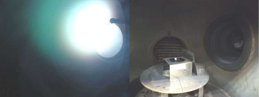
Рис. 1. Экспериментальная установка и процесс имитации импульсного теплового воздействия
Fig. 1. Experimental setup and process of simulating pulsed thermal action
The experimental part of the study additionally included electron microscopic studies of samples exposed to pulsed infrared radiation to determine the density of the defect network, types of defects, their clusters and other damages. The results obtained showed the presence of a significant defect density in all samples up to 1.019 cm–3. At the same time, the defect density in the thin CdTe film was lower. The defects were represented mainly by vacancies and interstitial atoms, dislocations and dislocation loops, as well as stacking faults (Fig. 2). Additional information on sample preparation and examination on a transmission electron microscope is presented in [5; 10; 11].
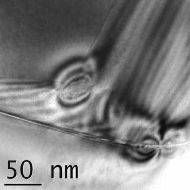
Рис. 2. Формирование дефектов в теллуриде кадмия после кратковременного теплового воздействия
Fig. 2. Formation of defects in cadmium telluride after short-term thermal exposure
Model of defect formation in cadmium telluride under pulsed thermal action
The theoretical work was based on the refinement of the mathematical model of physicochemical transformations in CdTe under pulsed action of infrared radiation with an amplitude of 1.000 Cº for no more than 10 s. The pulse was modeled using the formula (Gaussian bell):
T = 27 ° С + A ■ exp( - 1 2), where A = 1.000 C°.
The calculation was performed using the Maple mathematical package.
The improved model of physicochemical transformations in semiconductors under the action of thermal radiation was based on a system of modified equations for the evolution of concentrations of structural point and double defects:
3 n 3 2 n
— = P + D I ^y — c о R ( nv + 2 nw - 2 vm ) — 2 c о A I ( n 2 + nm ) + 2 Pm ,
d v 3 t
|
2 P + DV ; " d z |
- c 0 R ( nv - 2 nw + 2 vm ) - 2 c 0 A V ( v 2 + vw ) + 2 Pw, |
(2) |
|
5 m 5 1 |
= c 0 A I ( n 2 - 2 nm ) - 2 c 0 Rvm - Pm , |
(3) |
|
5 w 5 1 |
= c 0 A V ( v 2 - 2 vw ) - 2 c 0 Rnw - Pw , |
(4) |
where t is the time; z is the distance from the surface to the middle of the film (film thickness is 200 nm). For effective concentrations, the following notations are introduced: CI and CV are the concentrations of interstitial atoms and vacancies; C m and C w are the concentrations of diinterstitials and divacancies; c 0 is the concentration of ideal cadmium telluride lattice sites. The calculation results are presented in terms of relative concentrations: n = C I / C o , v = CV I c о , m = Cm I C o , w = C W I C o . Notations for model parameters: DI and DV are the diffusion (migration) coefficients of interstitial atoms and vacancies; AI and AV are the agglomeration (attachment) coefficients of interstitial atoms and vacancies, respectively; R is the recombination coefficient; P is the crystal lattice dissociation coefficient corresponding to the effective energy of thermal Frenkel pair production EP .
All the listed coefficients are expressed through the activation energies of the reaction as
( R , A I , A V ) = a 3v ■ exp
I- ( E R ’ E i ’ E v ) 1 ’
V kT J
( DI , D V ) = a 2 V ■ exp I - TV ( E Im , E Vm ) V kl
P
= v- exp I -

here v is the frequency of oscillations of the crystal lattice; a is the lattice constant; k is the Boltzmann constant; T is the temperature. To solve the equations, it is necessary to take into account diffusion, which affects thin films more significantly than macroscopic samples. The numerical values of the parameters used in expressions (1) – (7) are presented in Table 2.
Table 2 Numerical values of a number of parameters of the CdTe crystal [5; 6; 12–15]
|
Er Im |
EVm |
E I |
E V |
E R |
E P |
c 0 |
v |
a |
|
eV |
eV |
eV |
eV |
eV |
eV |
сm-3 |
Hz |
nm |
|
0.32 |
0.6 |
0.45 |
0.5 |
0.25 |
1.4 |
1.5∙1022 |
1013 |
0.648 |
Solutions of equations (1) – (7) are presented in Fig. 3.
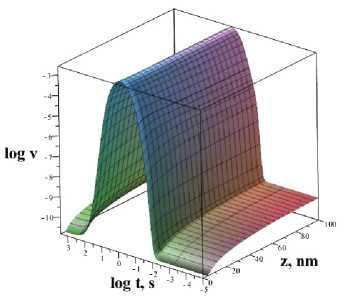
Рис. 3. Зависимость концентраций точечных дефектов (вакансий и междоузлий) от времени и расстояния от поверхности до середины кристаллической пленки при кратковременном тепловом воздействии с амплитудой до 1000 °С
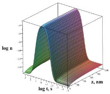
Fig. 3. Dependence of concentrations of point defects (vacancies and interstitials) on time and distance from the surface to the middle of the crystalline film under short-term thermal exposure with an amplitude of up to 1,000 °С
The obtained results (Fig. 3) show good agreement with the experimental data. High temperatures, even acting briefly on cadmium telluride, definitely lead to explosive growth and evolution of the defect network with a concentration of the order of 1.019 cm–3 and subsequent destruction of the material. However, studies show that thin-film CdTe samples tend to cool more quickly and reduce the concentration of point defects due to the emergence of some of them on the surface, which reduces the probability of combining into clusters.
Conclusion
A comprehensive study of pulsed thermal effects on a detector made of cadmium telluride was conducted. An increase in detector temperature from 27 to 1.027 ºС was considered. The heating can be caused by exposure to sunlight, infrared radiation during a short circuit near the detector, direct heating of the detector during voltage surges in the power supply network, and pulsed radiation exposure. The study showed that crystalline material quickly degrades under such extreme conditions due to the rapid evolution of the defective network. At the same time, thin-film CdTe samples are more resistant to pulsed thermal effects, and equipment based on them is able to maintain working condition much longer.
The mathematical model, on the basis of which the numerical results were obtained, is a good addition (as an initial condition) to the models describing the evolution of point defects under ionizing radiation.
References Specificity of defect formation in detectors based on cadmium telluride under pulsed thermal influence
- Elyash S. L., Rodigin A. V., Loiko T. V., Polyakov A. I., Kapitanov S. V. CdTe detectors for recording X-ray pulses with subnanosecond resolution. Instruments and experimental technique. 2011, No. 4, P. 116–119.
- Zaveryukhin B. N., Mirsagatov Sh. A., Zaveryukhina N. N., Volodarsky V. V., Zaveryukhina E. B. [Film detectors of nuclear radiation from cadmium telluride]. Letters to the Journal of Technical Physics. 2003, Vol. 29, Iss. 22, P. 80–87 (In Russ.).
- Cavallini A., Fraboni B., Auricchio N., Caroli E., Dusi W., Chirco P., Morigi M.P., Zanarini M. Irradiation-induced defects in CdTe and CdZnTe detectors. Nuclear Instruments and Methods in Physics Research Section A: Accelerators, Spectrometers, Detectors and Associated Equipment. 2001, Vol. 458, Iss. 1–2, P. 392–399.
- Kondrik A. I., Kovtun G. P. [Influence of radiation defects on the electrophysical and detector properties of CdTe: Cl irradiated with neutrons]. Tekhnologiya i konstruirovanie v elektronnoy apparatury. 2020, No. 1–2, P. 22–29 (In Russ.).
- Loginov Y. Y., Brown P. D., Durose K. Zakonomernosti obrazovaniya strukturnykh defektov v poluprovodnikakh A2V6 [Regularity of the structural defects’ formation in semiconductors A2B6]. Moscow, Logos Publ., 2003, 304 p.
- Mozzherin A. V., Paklin N. N. [Heat resistance of devices based on cadmium telluride in fires under conditions of variable temperature]. Pozharnaya bezopasnost'. 2023, No. 2 (111), P. 42–48 (In Russ.). https://doi.org/10.37657/vniipo.pb.2023.111.2.003.
- Loginov Yu. Yu., Mozzherin A. V., Bril’kov A. V. Dependence of the Critical Radius of Partial Dislocation Loops on the Stacking Fault Energy in Semiconductors. Physics of the Solid State. 2014, Vol. 56, No. 4, P. 720–722.
- Fizika i khimiya soedineniy A2V6 [Physics and Chemistry of A2B6 Compounds]. Ed. S. A. Medvedev. Moscow, Mir Publ., 1970, 624 p.
- Sultonov N. S., Khamrokulov R. B., Akobirowa A. T. [Development of Technology for Obtaining Polycrystalline Cadmium Telluride Films and Study of Their Structure and Electrical Properties]. Vestnik TNU. 2020, No. 4, P. 130–146 (In Russ.).
- Kobeleva S. P. [Structure of Intrinsic Point Defects in CdTe]. Matematicheskoe modelirovanie v materialovedenii elektronnykh komponentov: materialy IV Mezhdunar. konf. [Mathematical Modeling in Materials Science of Electronic Components: Proceedings of the IV International Conference]. Moscow, 2022, P. 135–138 (In Russ.).
- Rai R. S., Mahajan S., McDevitt S., Johnson C. J. Characterization of CdTe, (Cd, Zn) Te, and Cd (Te, Se) single crystals by transmission electron microscopy. J. Vac. Sci. and Technol. 1991, Vol. B9, No. 3, P. 1892–1896.
- Loginov Y. Y., Mozzherin A. V., Paklin N. N. Particularities of the interstitial atoms and vacancies clusters formation in a thin cadmium telluride foil during in situ electron irradiation in a TEM. IOP Conf. Series: Materials Science and Engineering. 2022, Vol. 1230, P. 012013. Doi: 10.1088/1757-899X/1230/1/012013.
- Gorichok I. V. [Enthalpy of Schottky Defects Formation in Semiconductors]. Physics of the Solid State. 2012, Vol. 54, P. 1373–1376 (In Russ.).
- Glas F. A simple calculation of energy changes upon stacking fault formation or local crystalline phase transition in semiconductors. Journal of Applied Physics. 2008, Vol. 104, 093520, P. 1–6.
- Smirnov A. A., Kaplunov I. A., Olnev A. A., Nikiforova A. N. [Development of a mathematical model of the process of charge collection and spectrum formation in detectors based on CdTe (CdZnTe) under gamma-ray irradiation]. Fiziko-khimicheskie aspekty izucheniya klasterov, nanostruktur i nanomaterialov. 2017, No. 9, P. 465–474 (In Russ.).
