Studies on the Necessity to Integrate the FPGA (Field Programmable Gate Array) Circuits in the Digital Electronics Lab Didactic Activity
 Circuits in the Digital Electronics Lab Didactic Activity")
Author: Corina Daniela Cunţan, Ioan Baciu, Mihaela Osaci
Journal: International Journal of Modern Education and Computer Science (IJMECS) @ijmecs
Article in issue: 6 vol.7, 2015.
Free access
The FPGA (Field Programmable Gate Array) circuits contain programmable logic components and are increasingly popular in implementing the applications for obtaining and processing signals. FPGA represents a modern development trend in digital electronics. The integration in the work with students of this trend is a difficult task, but also useful, because many students face problems when they must use a design environment. The application of FPGA technology can be useful to students either for the laboratory work on advanced topics, or for obtaining skills to use an industry standard design environment. The purpose of this paper is to conduct studies on the need to integrate the FPGA digital electronics trend in the laboratory didactic activity of the students. As case study, we present the design of a control circuit and its implementation in a FPGA, i.e. on a Basys2 board with Xilinx programming environment.
FPGA circuits, laboratory didactic activity, programmable logic components, digital electronics, Xilinx programming environment
Short address: https://sciup.org/15014763
IDR: 15014763
Text of the scientific article Studies on the Necessity to Integrate the FPGA (Field Programmable Gate Array) Circuits in the Digital Electronics Lab Didactic Activity
The students’ motivation to study the discipline Digital Electronics is not an easy task [1], given the accelerated progress in the field and the cost of laboratory equipment to be borne by the universities.
Regarding the Digital Electronics discipline, there are two ways of working [1]: with real integrated circuits, professional equipment for signal generation and visualization, and the modality that involves virtual instrumentation, development environments with reprogrammable devices, circuit simulation software and HDL simulators (hardware description language).
The modality to combine the two methods in the teaching activity creates to the student (future engineer) adequate conditions to learn skills either in design or in the implementation of practical experimentation and troubleshooting, skills that will facilitate the career success.
A field-programmable gate array (FPGA) is an integrated circuit designed to be configured by a customer or a designer after manufacturing. Many complex electronic systems are based on the FPGAs, whose applications are found everywhere. Being a lot of devices and families from different manufacturers, the FPGA fundamentals and characteristics are difficult to explain. For this reason, it is important to have certain tools available, intended to facilitate the learning process of the FPGA fundamentals and the design of systems based on them. The current FPGAs include very complex embedded digital blocks or memory blocks thanks to the circuit fabrication progress. The learning system provides the hardware and software tools with a tutorial, the friendly interface with the computer succeeding to facilitate the FPGA distance learning for the students with a basic knowledge of digital electronics and VHDL (VHSIC Hardware Description Language) [2].
Thanks to the reconfiguration specialty and the free service of design simulator programs, the FPGAs gained an important role in the electronics engineering teaching and became one of the most useful devices of the design laboratories. Nowadays, many Electronics and Computer Engineering Departments of the universities worldwide are using the FPGAs as education material, besides the engineering applications [3].
Because the university professors’ purpose is to provide the students with a good practical experience of the techniques used in modern digital system design in addition to their solid theoretical background, by using the FPGAs as a hardware platform and VHDL as a design language, the students will have a whole picture of the digital system design methods and a theoretical and practical knowledge of the digital devices, tools, data networks and operating systems. The acquired ability to learn new techniques and new developments in industrial and/or research applications, the experience to work in a team and to use the industry-standard tools, and the practical experience in various stages of the design of a modern digital system and even in the construction of a complex device, are all going to make the current students attractive candidates for the employers in the field.
-
II. The FPGA Technology
The FPGA (Field Programmable Gate Array) circuits are generic circuits that can be programmed to implement any user-defined function. A FPGA consists of an array of programmable blocks, an interconnection network that connects these blocks to each other, I/O circuits and a SRAM memory that configures these structures [4].
The FPGAs provide to the user a wide range of configurable resources that can implement a variety of arithmetic and logical functions. These resources include: dedicated DSP blocks (digital signal processing), registers, tri-state buffers, multiplexers, and demultiplexers.
The FPGA circuits are devices with very good data processing performance [5], [6], [7]. The DSP performance is derived from the FPGA’s capacity to build parallel architectures, in contrast to the microprocessors or DSP processors, where the performance is determined by the clock pulse frequency. The FPGA’s performance is directly proportional to the parallelism that can be implemented to run a certain algorithm.
The new improvements in the FPGA technology have introduced multiple options for the digital signal processing applications, which require high performance and low cost of development and production.
The FPGA Spartan-3 family [8] of circuits has been designed specifically to meet the demands of high capacity and low cost, specific to the commodity market. The architecture of Spartan-3 family is based on the architecture of its predecessor, Spartan-IIE, having the additional advantage of extra logic resources, increased capacity of internal RAM, increased number of I/O pins, improved clock signal management resources. The new features are taken from the upper class of the FPGA circuits made by XILINX, the Virtex-II family. The improvements brought to the Spartan-3 family of circuits, combined with advanced manufacturing processes, provide enhanced functionality and very good price / performance ratio, setting new standards in the field of programmable logic circuits.
The FPGA Basys2 circuit is built on the platform of Xilinx Spartan-3E and is a product of Digilent Inc. It is a FPGA of medium complexity, intended for initiation in reconfigurable circuits programming, and not only (Fig. 1). It contains all the basic features of BASYS and, in addition, it enables the user to experience the new Adept 2.0 from Digilent Inc. [9], [10].
Basys 2 contains a number of resources that can be easily used in circuit designing. All these resources are connected to the FPGA pins, as shown in Fig. 1.
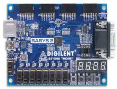
Fig.1. FPGA Basys2 [7].
-
III. Programming Of Basys2 Development Board
The XILINX ISE software environment for designing (i.e. Integrated Software Environment) is used to fully create and implement a project for the programmable structures of XILINX type [11]. The content of ISE Project Navigator software facilitates the creation of the project, organizing it step by step [4]: description, synthesis, implementation, verification and configuration. After generating the programming files (bitstream file), the designer has the possibility to program the reconfigurable circuit. During the configuration process, the interconnections of the chosen FPGA structure are programmed.
The VHDL (VHSIC HDL - Very High Speed Integrated Circuit Hardware Description Language) is a language for describing the hardware, intended for the description of the behaviour and/or architecture of a logic electronic "module", i.e. a combinational logic and/or sequential function. The VHDL, besides the Verilog language, is the designing language mostly used for digital electronic systems, being one of the most important tools for designing the modern integrated circuits, used also for microprocessors (DSP, graphics accelerators), in telecommunications (TV, mobile phones), cars (navigation, stability control systems), and others. The VHDL standard appeared in 1987, and is referred to as "IEEE 1076". It is used in the computer-aided design of integrated circuits and for FPGA configuration.
The VHDL allows the description of systems at a functional or structural level. The structural level describes a system as a collection of logic gates and components that are connected so as to realise the desired function; that's why it can be compared with a diagram of interconnected logic gates. This is a representation closer to the physical realization of the system. The functional level specifies the relationships between the input and output signals. The functional level can be divided into two representation styles: Data Flow and algorithmic. The data flow representation describes how the data are flowing through the system, and is made in terms of data transfer among registers (RTL – Register Transfer Level). The instructions are concurrent, being executed in parallel when the data are present at the input. In the algorithmic representation, the instructions are sequential, being executed in the order specified by the programmer. The VHDL allows assignment of signals in both ways (sequentially or concurrently). [4]
For working, a file in VHDL language will be first introduced in the XILINX ISE environment, which will be written using the editor of XILINX software [12]. In any project it is required to use constraints to meet the requirements on propagation time, occupied area and pin assignment. For this purpose, there are three possible types of constraints [12] . The XILINX ISE development environment runs automatically the synthesis process and creates a User Constraints File (UCF), which is subsequently attached to the project. [4] After the project was completed & verified, and the constraints files were added, the project can be synthesized and then implemented to realise, in the end, the programming of the reconfigurable structure. If the process did not generate errors, the first report can be viewed on the digital module.
-
IV. Design, Implementation And Operation Verification Of A Control Circuit
The designed circuit allows obtaining rectangular pulse sequences on six different channels, in order to obtain simultaneously three signals on 1 and the other three on 0. For this, we used the clock signal of the development board, whose frequency is reduced by using a divider circuit realised in VHDL code (Fig. 2).
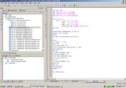
Fig.2. The VHDL code for the frequency divider
Through the divider circuit, we obtain the desired control frequency. Also from the divider circuit we obtain the clock signal for the counter, comparators and multiplexers.
To obtain the operating frequency, we use the clock circuit of the Basys 2 board, whose frequency is divided according to (1):
ft = fdOck/n (1)
where n represents a division number chosen in such a way to match the desired output frequency. For example, for a frequency of 1 kHz, n = 50000000.
The counter (Fig.3) is a three-bit asynchronous counter made with T-type flip-flops. The counter circuit has been completed with a circuit for the identification of the 6th status (110), which initializes its status.
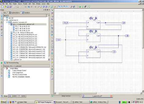
Fig.3. Three-bit asynchronous counter realised in Xilinx
For obtaining the six sequences desired, it was necessary to complete the counter with a circuit for the identification of the 6th status (Fig.4)., which initializes its status (2),
ResetR = QB • Qc
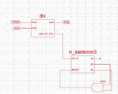
Fig.4. Three-bit counter with circuit for identification of the 6th status
For each counter output sequence, the comparator selection is made by means of the control logic. [13] (Fig. 5). The output of each comparator has six bits, corresponding to the binary representation of the decimal figures: 42, 14, 28, 21, 49 and 35. The outputs of the first comparator are connected to the first input of each multiplexer. The outputs of the comparator 2 are connected to the second input of each multiplexer. The outputs of the other comparators are connected following the same logic. So, at the first selection, at the output “000” of the counter shall be selected the comparator 1 and input 1 of each multiplexer, obtaining the adequate command of the three transistors of the bridge inverter.
Based on the same algorithm, there are selected each comparator and the next of the multiplexers, thus obtaining the six control sequences.
The selection of comparators is made according to (3) -
(8), presented below.
Sa = Qa + Qb + Qc(3)
Sb = Qa + Qb + Qc(4)
Sc = Qa + Qb + Qc(5)
Sd = Qa + Qb + Qc(6)
Se = Qa + Qb + Qc(7)
Sf = Qa + Qb + Qc(8)
We made six comparators in VHDL code [14], each comparator having entered in its structure the code corresponding to the sequence desired to be obtained at the output (Fig. 6).
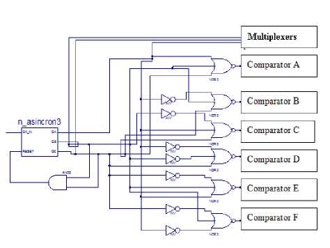
Fig.5. The logic structure for comparator selection
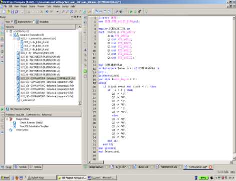
Fig.6. The VHDL code for the comparator “A”
The comparator outputs are connected to the inputs of six multiplexers which are controlled by the counter output sequence (Fig.7).
The multiplexer selection is made through a logical structure, according to (9) and (10), which receives the command from the counter output [15].
M1 = Qa • Qb • Qc ' C11 + Qa ' Qb ' Qc ' C 21
+ Qa • Qb • Qc ' C31 + Qa ' Qb ' Qc ' C41 +
+ Qa • Qb • Qc ' C51 + Qa ' Qb ' Qc' C
M6 = Qa • Qb • Qc ' C16 + Qa ' Qb ' Qc ' C26
+ Qa • Qb • Qc ' C36 + Qa ' Qb ' Qc ' C46 +
+ Qa • Qb • Qc ' C56 + Qa ' Qb ' Qc 'C where Cij represents the output “i” of the comparator “j” and M1…M6 are the inputs of the multiplexers.
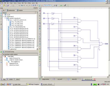
Fig.7. The multiplexer realised in Xilinx
Each of the six output states of the counter enables the selection of different sequence. The multiplexer outputs are brought to the output pins of the Basys 2 board, as well as to the LEDs available on the development board, to visualize the obtained sequences [15].
From the above, we can obtain the complete diagram, which allows obtaining the control sequence at the output connectors of the board.
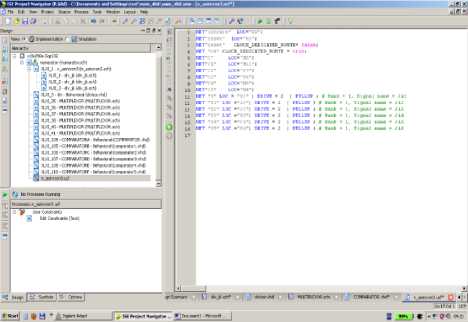
Fig.8. Constraints applied to the pins of the FPGA circuit
To test the diagram on the development board, each input and output terminal is associated with a pin of the FPGA circuit. For example, the inputs are connected to the switches, and the outputs are connected to the LEDs and control pins. This is realised through a file with the extension .ucf ( User Constraints File ), containing an association between the input/output ports and the pins of the FPGA circuit (Fig.8).
-
V. Experimental results
The circuit operation was verified by optical visualization on the LEDs available on the development board. At low frequencies, the output sequences can be seen directly by the human observer (Fig.9), and at higher frequencies (>50 Hz), the LEDs will be perceived as permanently lit (Fig.10).
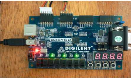
Fig.9. Obtaining of the first sequence on the Basys2 board
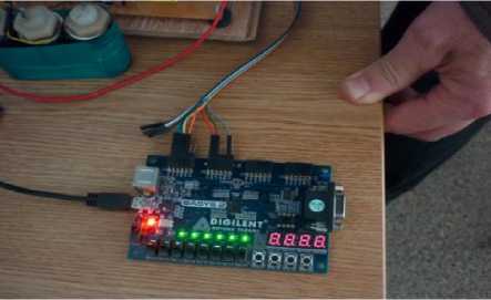
Fig.10. Operation of the circuit at high frequency
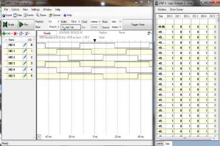
Fig.11. Output sequences
To visualize the output sequences, we used the logic analyzer found in the Electronics Explorer module from Digilent Inc., module that enables simultaneous visualization of the six output sequences. The six output sequences are presented (Fig. 11) in graphical form and as numerical sequence. The measurements were made at frequencies up to 10 KHz. The circuit can also provide pulses with frequency higher than 10 KHz.
The signals obtained at the development board output have been used (Fig. 13) to control a bridge inverter [16], [17], with insulated-gate bipolar transistors (IGBT) (Fig.12).
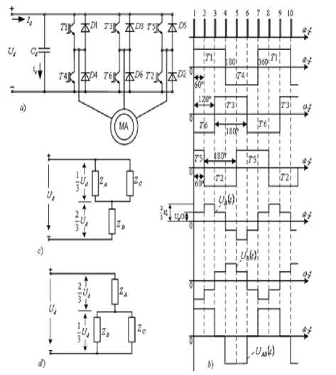
Fig.12. The three-phase voltage inverter a) Three-phase bridge with transistors; b) Waveforms d) Modality to connect the load impedances
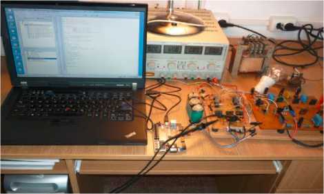
Fig.13. Verification of the control circuit operation
Examining the waveforms, it is noted that, in the same time interval, two voltages have the same polarity and the third one has opposite polarity. This requirement is met if there are conducting, at any time, two transistors located at the top of the bridge and one at the bottom, or two transistors located at the bottom and one at the top.
For example: On the first interval, UR and UT > 0, and US < 0; this is realised if T1, T5, T4 are conducting.
Table 1. Operation of the thyristors
|
Time interval T |
1 |
2 |
3 |
4 |
5 |
6 |
|
T 1 |
X |
X |
X |
|||
|
T 2 |
X |
X |
X |
|||
|
T 3 |
X |
X |
X |
|||
|
T 4 |
X |
X |
X |
|||
|
T 5 |
X |
X |
X |
|||
|
T 6 |
X |
X |
X |
From the above table, we can see that each thyristor is conducting for a half-period, and then the control voltages must be applied to the pulse transformers corresponding to the thyristors that have conducted for locking them.
Considering the consumer symmetrical, with Z S impedance per each phase, we can calculate the voltage steps from which the voltage per one phase consists of:
3EZs3EZs
(UR) = 7 = ” Л ' ч = E(UT)1 (11)
Z, + Z s 2 3 Z. 2
(U s ) 2 =
3E z s
Zs + -s s2
= 2 E
The six pulse trains were amplified and passed through a galvanic separation circuit, and then were brought in the grids of the IGBT transistors.
The control sequence that corresponds to the transistors must comply with the following sequence to entry into conduction. Thus, the control circuit will provide pulses in the transistors grids, in the following order:
-
- The first sequence obtains at output the binary conversion of the decimal number 42 (the pulse for sequence 1- 101010) and controls the transistors T1, T6 and T5;
-
- The second sequence obtains at output the binary conversion of the decimal number 14 (the pulse for sequence 2- 001110) and controls the transistors T1, T6 and T2;
-
- The third sequence obtains at output the binary conversion of the decimal number 28 (the pulse for sequence 3- 011100) and controls the transistors T1, T3 and T2;
-
- The fourth sequence obtains at output the binary conversion of the decimal number 21 (the pulse for sequence 4- 010101) and controls the transistors T4, T3 and T2;
-
- The fifth sequence obtains at output the binary conversion of the decimal number 49 (the pulse for
sequence 5- 110001) and controls the transistors T4, T3 and T5;
-
- The sixth sequence obtains at output the binary conversion of the decimal number 35 (the pulse for sequence 6- 100011) and controls the transistors T4, T6 and T5.
-
VI. Conclusions
In terms of teaching, the two ways of working in Digital Electronics (real and virtual) show advantages and disadvantages. The use of real equipments, signals and circuits shows advantage, because it allows the presentation of real-life testing and troubleshooting issues in electronics (hardware engineering), but the disadvantage of this way is the high cost, real space occupied in the laboratory and students’ impossibility to have online access during carrying out the experiment. The virtualization is a good thing for quick and easy understanding of the concepts (hardware designer) [18], [19], [20], [21].
The Xilinx software has many advantages, including flexibility, i.e. the possibility to change data in the course of a project, an example in this regard being the possibility to periodically change the clock in the VHDL code of the counter. Thus, the time counting is changing. Another advantage is that it’s relatively easy to realise projects by using the library of this software, high programmability and short time for product design and presentation on the market.
The main inconvenient of the VHDL language is its complexity. Therefore, the designers need thorough knowledge of programming. A great advantage would be the fact that it has an IEEE standard recognized by all the manufacturers.
Approaching the basic digital circuits on simulator seems to be very convenient, either as cost (for the education institution) or as acquisition of design experience by the students. Also, the students can have online access to the laboratory works. As disadvantage, we mention that the "simulation experience" is not enough to realise and troubleshoot the real digital integrated circuits.
Given this analysis, we conclude that, in terms of teaching, a choice that conveniently combines the two ways of working in Digital Electronics is beneficial for the current stage of evolution in the field and in the teaching process. Certainly, the accelerated progress in the Digital Electronics field requires adapting to the current trends also in the teaching activities, for the so formed engineer to be competitive in the labour market.
References Studies on the Necessity to Integrate the FPGA (Field Programmable Gate Array) Circuits in the Digital Electronics Lab Didactic Activity
- D. Nicula, "Digital Electronics: a Modern Lab Approach", Bulletin of the Transilvania University of Braşov, Series I: Engineering Sciences, Vol. 4 (53) no. 1, pp. 135-142, 2011.
- C. Quintans, M.D. Valdes , M.J. Moure, L. Fernandez-Ferreira, E. Mandado, "Digital electronics learning system based on FPGA applications", Frontiers in Education, 2005, [FIE '05. Proceedings 35th Annual Conference].
- V. Kiray, M. K. Zhaparov, "FPGA Based Digital Electronic Education, Clock-Calendar Design", Przegląd Elektrotechniczny, no.4, R. 89, pp.185-189, 2013.
- "Introducere în familia de circuite Virtex." [Online] Available at: http://ebookbrowsee.net/curs-10-pdf-d54593424.
- J.M. Ramirez Cortes, P. Gomez Gil, V. Alarcon Aquino, J. Martinez Carballido, E. Morales Flores, "FPGA based educational platform for real time image processing experiments", Computer Application in Engineering Education, vol. 21, Issue 1, pp. 193-201, 2013.
- P. Bulić, V. Guštin, D. Šonc, A. Štrancar, "An FPGA-based integrated environment for computer architecture", Computer Applications in Engineering Education, vol. 21, Issue 1, pp. 26–35, 2013.
- Y. Kong, I. Xie, "Professional Courses for Computer Engineering Education", I. J. Modern Education and Computer Science, 1, pp.1-8, 2010.
- B. Rashidi, "Low-Cost and Optimized Two Layers Embedded Board Based on ATmega32L Microcontroller and Spartan-3 FPGA", I.J.Modern Education and Computer Science, 3, pp.56-68, 2013.
- "Manual de referencia de la tarjeta BASYS 2" [Online].Available:http://neirol-vm-51.die.upm.es/~profes/celt/1213/public/docs/Manual%20de%20referencia%20BASYS%202.pdf.
- [Online]. Available: http://www.digilentinc.com.
- "Xilinx Inc. Vertix-5 FPGA User Guide. [Online] Available:http://www.xilinx.com/support/documentation/user_guides/ug190.pdf.
- G.V. Iana, G. Şerban, L. Ionescu, P. Anghelescu, Programarea cu limbaje de descriere hardware, Bucharest, Publisher: Matrix Rom, 2010.
- B. Rashidi, B. Rashidi, "Implementation of an Optimized and Pipelined Combinational Logic Rijndael S-Box on FPGA", I. J. Computer Network and Information Security, 1, pp. 41-48, 2013.
- G. Grover, I. Chaudhary, "Implementation of Particle Swarm Optimization Algorithm in VHDL for Digital Circuits Optimization", I.J. Information Engineering and Electronic Business, 5, pp. 16-21, 2014.
- N. Grover, M.K.Soni, "Reduction of Power Consumption in FPGAs - an Overview", I.J. Information Engineering and Electronic Business, 5, pp. 50-69, 2012.
- B. Rashidi, "FPGA Implementation of Digital Controller for Simple and Maximum Boost Control of Three Phase Z-Source Inverter", I.J. Information Technology and Computer Science, 04, pp.85-95, 2013.
- B. Rashidi, M. Sabahi, "High Performance FPGA Based Digital Space Vector PWM Three Phase Voltage Source Inverter", I.J.Modern Education and Computer Science, 1, pp.62-71, 2013.
- Z. A. Obaid, N. Sulaiman and M.N. Hamidon, "FPGA-based Implementation of Digital Logic Design using Altera DE2 Board, International Journal of Computer Science and Network Security, vol.9, no.8, pp. 186-194, July 2009.
- J. García-Zubía, I. Angulo, L. Rodriguez-Gil, P. Orduna, O. Dziabenko, M. Güenaga, "Boole-WebLab-FPGA: Creating an Integrated Digital Electronics Learning Workflow Through a Hybrid Laboratory and an Educational Electronics Design Tool", International Journal of Online Engineering, vol. 9, Special Issue 8: "Exp.at'13", pp. 19-22, December 2013.
- Kiray V., "FPGA Based Digital Electronic Education, Data Entry Organization for a Calculator", Przegląd Elektrotechniczny, R. 88, nr 11a, pp. 200—204, 2012.
- A. Vera, J. Quiñones, E. Enriquez, S. Arenas and A. Bernal, "Remote Laboratory for e-Learning of Digital Systems Design", Asian Transactions on Fundamentals of Electronics, Communication & Multimedia, vol. 02, Issue 05, pp. 1-10, 2012.
