System Design of a Trusted SoC and Detailed Analysis of its Secure State Transitions

Author: Xianwen Yang, Luguo Zhang, Zheng Li, Shixiong Zhu, Wenzheng Zhang, Yongqi Lv
Journal: International Journal of Computer Network and Information Security(IJCNIS) @ijcnis
Article in issue: 1 vol.2, 2010.
Free access
According to the relevant criterion and principle for designing and evaluating various trusted computing chips, we have proposed a new trusted SoC chip, and have given the implementation of its basic functional modules. In detail, we have discussed the design of the trusted SoC security architecture and the main module functional modules such as microprocessor, cryptographic function module, security management module, input/output interface, along with the most important memory management unit. Moreover, we have discussed reliability of relevant parameters and transfer strategy for trusted root in chip development and application, together with the simulation and validation of corresponding functions. At last, we point out that one of the most important further research directions is the trusted measurement of dynamic data and software running in security environment.
SoC, COS, security system design, trusted measurement, trusted transfer strategy
Short address: https://sciup.org/15010986
IDR: 15010986
Text of the scientific article System Design of a Trusted SoC and Detailed Analysis of its Secure State Transitions
Published Online November 2010 in MECS
Current information systems include a great deal of sensitive information that needs to be protected. Hence, the need to secure these systems is recognized by academics and practitioners alike. Information security has become an increasingly important aspect in developing distributed systems, especially in the military domain and electronic business sector [1, 2]. Because failures of security mechanisms may cause very high potential damage, the correctness of such systems is crucial. The three big security aspects that can be formulated are confidentiality, meaning that only authorized entities must be able to read confidential data, integrity, stating that no unauthorized entity must be able to change data without being detected and availability, mandating that data is on-hand when it is needed. To achieve these goals, secure System-on-Chip (SoC from now on), which is playing a special role in these new security strategies, is increasingly prevalent, e.g.
This work was supported by the Natural Science Foundation of China under Grant No.61072047 and the National Modern Communication Laboratory Foundation of China under Grant No.9140C1106021006
hundreds of millions of smart cards (which can be viewed as typical secure SoCs) are used today in thousands of applications which include computer access control, identification cards, credit cards, etc. [1, 2, 3].
With the purpose of promoting the popularization and application of trusted computing technology, State Password Administration of China has published “Support platform and interface criterion of trusted computing cryptography technology”, which has defined the trusted compute platform architecture as “On the basis of cryptograph technology, realizing the security function of platform integrality, trusted identity, data security and so on”, and the supporting relationship of cryptograph platform function and trusted cryptography module structure is presented.
Based on the instruction of criterion, according to the development module of computation and evaluation object in Common Criteria (namely CC) and the derived provision for evaluation object security requirement and function criterion [4], and referring the TPM-PP principle [5,6] and the relevant trusted computed criterion published by State password administration[7], a trusted SoC chip based on ETI 8051 microprocessor is developed, it possess the following basic function.
-
• provide digital signature/identification and identity discerning;
-
• provide high-speed data encryption and decryption;
-
• provide data hash value compute function;
-
• support chip internal key generation;
-
• support COS and application reconstruction;
-
• support classification startup and trusted chain transfer;
-
• support preventing insert and plug or sudden power cut off, ensuring the atomicity of function service.
And the relevant function of the design SoC chip is simulated and validated, the result indicated that it accord with the relevant provision and demand of trusted computed platform. This paper focused on discussing the design of trusted SoC chip security architecture and trusted measurement and transfer strategy of the chip.
This paper is structured as follows: Section 2 describes sketches the architecture of our dedicated secure SoC and explains some main modules, such as microprocessor, cryptographic function module, security management module, input/output interface, and the most important RAM management unit. Section 3 introduces the secure schemes for assets management and protection are defined detailed, while how to use the schemes to achieve the security in state transitions is discussed meantime. Section 4 remarks some experimental proof for practical applications of the chip. Finally, Section 5 concludes the paper and introduces future directions.
-
II. SECURITY ARCHITECTURE DESIGN OF A TRUSTED SOC
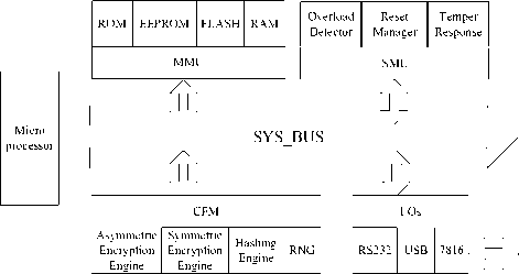
Figure 1. System architecture of a secure trusted SoC.
The trusted SoC security architecture is depicted in Fig.1, and it consists of microprocessor, memory management unit (MMU), security management logic (SML), input/output interfaces (I/Os) and cryptography function module (CFM) and so on [8]. Under the system initial state startup and the control of monitor software, it accomplished credibility lead, integrality test and measurement, identity discerning and authentication, the security storage of key, certificate and other sensitivity information, and the security download, integrality measurement and credibility lead and transfer of user internet applications and chip operating system (COS) .The following subsection has a brief introduction to the function of CFM, SLM and MMU.
A. Microprocessor
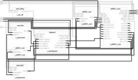
Figure 2. RTL schematic diagram of ETI 8051.
In this paper we takes the ETI 8051 IP core shown in Fig. 2 into our secure SoC as the main microprocessor, which has complete abilities to run program code effectively and manage the internal data low-costly for different modules. Since the original open source is derived from the MCS 8051 project on the Opencore website, to be able to handle faults and work correctly [9], we have checked almost all logic faults of the original IP core under the support of Keil software and Modelsim simulator, and have given their corresponding modifications. After that, a variety of tests to the modified IP core is fulfilled based on the Altera Cyclone-II FPGA device. Conclusively, the modified ETI 8051 IP core runs normally, and achieves the complete functionalities for practical applications.
-
B. Cryptography function module
Cryptograph function module integrates six IP cores including RSA, ECC, AES, SHA-1 and random number generator, it is connected to system bus by IP bridging technology and dual-port memory [8]. Under the control of microprocessor, RSA and ECC IP cores provide digital signature, identity authentication, key exchange and data encryption and so on; AES and DES IP cores provide high-speed data encryption and decryption and MAC code generation and validation; SHA-1 IP core provide system with hash arithmetic support, realize the system integrality measurement, it is the key components of credibility startup and lead and the measurement of download software integrality; RNG IP core provide the system with well capability random number which is used for the conversation key negotiation of AES and DES arithmetic and the generation of fresh factor in communication protocol. The above cryptograph function components can entirely satisfy trusted computed
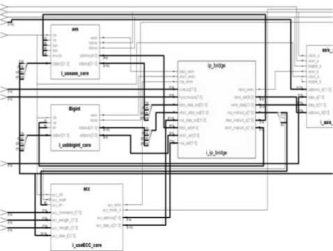
Figure 3. RTL schematic diagram of connecting different IP cores using IP bridge technology.
platform request for cryptograph service, and it is convenient for the replacement of cryptograph arithmetic IP core due to adopting the reconstruction logic interface circuit such as IP bridge technology shown in Fig. 3, which realize the connection of cryptograph arithmetic IP core.
-
C. Security management logic
Security management logic is consisted of crossboarder detect, attack defend and reset manage, it make up the chip security logic barrier. Cross-boarder detect combine with MMU realizing memory authority management of different zone, and ensuring that the readwrite of key and password satisfy the corresponding security management strategy; attack response module is consisted of variety transducer array and software attack check program, it check all kings of known physical attack and multi-logic attack, once detect relevant attack, startup the emergency response mechanisms, and according to undermine degrees of all kinds of attacks, for sensitive information store in chip do the following operation: destruction, invalidation, disabled, close application, close system and reset system and so on. Meanwhile, keep attacking type, time, consequence and the original record of response process for auditing afterwards; reset management module manage the cold boot reset, warm boot reset, attack response reset and run down reset and so on, and on the basis of previously defined priority, accomplishing the transaction of the corresponding reset signal, and provide good operability and controllability for system in the premise of system failure tolerance and usability.
-
D. Memory management unit
Memory management unit consists of memory bus configuration module, system operation state machine and memory, it accomplish the storage and security access control of all kinds of sensitive information and corresponding program. Memory contain ROM, EEPROM and FLASH, ROM store system self-test program, system lead program, software download monitor program, system state integrality measurement value in initial state and all programs hash values, and the identity key of chip manufacturer, chip serial number and the share secret data of developer and manufacturer, it is the original trusted root of chip system. EEPROM and FLASH respectively set initial layer, operating system layer, running state register ST correspond to user layer, configuration register group PCR correspond to each level chip function module and program and data integrality register group DIR, it store the integrality measurement value of relevant object, and satisfy the system security control demand. According to the three buses in storage zone of MCU operation state, system state and user state are respectively independent in logic, memory bus configuration module link to MCU, composing a memory subarea management module correspond to MCU operation state, and let each storage zone forming independent isolated logic zone correspond to operation state, composing storage zone firewall between different operation state. System operation state machine let system in operation process realizing the full flow control of the transition: initial state to system state, system state to user state and any state to initial state when each state operates stably and reset system. It insured that the operation state cannot change from super stratum to bottom layer, letting super stratum code have no operate authority to sensitive information belong to bottom code, trusted chain up deliver from trusted root.
The RAM of the secure SoC has been divided into seven parts. According to the importance and security level in practical use, the seven parts can be classified into four areas, which are tagged in Fig. 4 as level 0 area, level 1 area, level 2 area which are used for storing different value assets (code and data in each area respectively), and the system’s public data memory. When code stored in some level memory executes, the input data is firstly stored in public data memory. Thereafter, the intermedial data is stored in the data memory with the same level as the counterpart code memory. Finally, according to different security attributes, the result data is either provided for output via input/output interface or stored in the data memory of the public interface for system use.
Level 0 area
Level 1 area
Level 2 area
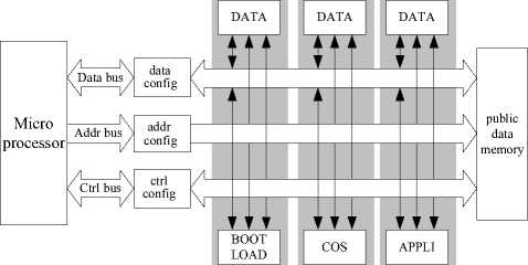
Figure 4. MMU architecture and its working principle
-
III. Secure operational states and constraint
CONDITIONS OF STATE TRANSITIONS
-
A. Secure operational states
After being delivered to the site where connected to a terminal, the chip can obtain different security authority, so it maintains in certain security state. There are several mutually-exclusive modes of operation in which the chip behavior may be limited. They are as follows:
-
• ST1: the initial state. The state is the trusted computing basis of the chip, and it consists of hardware logic, control code and data at lower level (e.g. in BIOS). Taking these as basis, the trusted property can be extended to the whole system of the chip.
-
• ST2: the enabled state. A manufacturer sells a chip to a customer. The manufacturer helps the customer take ownership (in the case of an unsophisticated customer) and is careful not to learn or remember the owner pass phrase. The customer chooses not to enable the chip. The secure operational state remains in ST2 except ownership has been transferred to the customer.
-
• ST3: the activation state. A manufacturer sells the chip bundled with a service contract. Service is outsourced to a company specializing in servicing this dedicated secure SoC. The service provider takes ownership and configures the platform to be safely managed. The activation state is left to the discretion of the customer.
-
• ST4: the load permission state of level 1 code. To satisfy the flexibility required in partial use of the chip, the level 1 code of the chip should be organized and configured by developer. The load
control program (i.e. Bootload) needs to authenticate the operation sponsor’s identity. If the authentication passes before expiration or timeout, the load permission flag of level 1 code is set.
-
• ST5: the loading state of level 1 code. Under the control of load control program, the input data will be taken as level 1 code in state ST5. During code loading, the SHA1 module will be employed to measure the integrity of level 1 code, and to compare with the provided integrity information of the input code. If the integrity is desired, the load completion flag of level 1 code is set.
-
• ST6: the running state of level 1 code. The chip can enter the running state of level 1 code from states of ST3 and ST5. Before entering the state, it needs to judge whether the load completion flag is valid, and after validating the integrity of level 1 code and data, the chip enters the running state in which relevant program is executed to fulfill certain purposes (e.g. control the load of level 2 code).
-
• ST7: the load permission state of level 2 code. The load of level 2 code should be achieved under the control of level 1 code. In the running state of level 1 code, if a user dispatches a command for loading level 2 code to the system, it needs to authenticate the sponsor’s identity under the control of level 1 code. If the authentication passes before expiration or timeout, the load permission flag of level 2 code is set.
-
• ST8: the loading state of level 2 code. Similar to the loading process of level 1 code, the load of level 2 code should be achieved under the control of load control program. Since the operating system helps enforce system integrity during code loading, level 1 code will engage corresponding components to do integrity measurement of level 2 code while storing its, and to compare with the incoming integrity information of the load code. If the integrity is desired, the load completion flag of level 2 code is set.
-
• ST9: the running state of level 2 code. After validating the integrity of level 2 code and data, the chip can enter ST9 from ST8 using state jump instruction or from ST6 using either state jump or call instruction. In the running state of level 1 code (ST6), the chip can arrive at level 2 code operations by call instruction of level 1 code, and it can return ST6 after the execution of relevant code. However, if it enters ST9 by state jump instruction, it can either maintain in ST9 or return ST3 by system resetting, but can no longer return ST6.
-
B. Control parameters and state flags
To implement the feasible transitions between different states mentioned above, some relevant control parameters and state flags are needed for indicating the control information and working states in the chip system. Control parameters indicate the integrity of the executing code and data, together with the reliability of different function modules. State flags indicate the current state of the system and the operation authority. With the aid of the two parts, the constraint conditions of state transitions, which result in the implementation of the security polices, is formed. Control parameters and state flags are the secure basis for constructing secure architecture of the chip, and based on the authority division of the chip, we take some memories in level 0 area to store control parameters and state flags of the secure SoC, more details of the arrangement is illustrated in Table I.
TABLE I.
C ontrol parameters and state flags
|
Name |
Length (Byte(s)) |
Address |
Brief Description |
|
OTP |
1 |
0000h |
One Time Programming |
|
STATE |
1 |
0001h |
State flag |
|
VERSION |
2 |
0002h~0003h |
Version information |
|
M_AUTH |
20 |
0004h~0017h |
Shared secret between manufacturer and developer |
|
M_PUBKEY |
128 |
0018h~0097h |
Public key of manufacturer |
|
SN |
20 |
0098h~00ABh |
Serial numble |
|
EK |
256 |
00ACh~01ABh |
Endorsement key |
|
AIK |
256 |
01ACh~02ABh |
Attestation identity key of developer |
|
PCRs |
20×8 |
02ACh~034Bh |
Platform configuration register |
|
DIRs |
20×3 |
034Ch~0387h |
Data integrity register |
|
USER_AUTH |
20 |
0388h~039Bh |
Shared secret between developer and user |
|
ERROR_SIG |
1 |
039Ch |
Counting errors occurring in authentication |
|
ATTACK_EVI |
3 |
039Dh~039Fh |
Memorizing attack behaviors |
|
RFU |
61 |
03A0h~03FFh |
Not used |
There into, one time programming (OTP) is used for one time setting of authority flag and state memory. STATE is the state flag of the chip, and it is used to indicate current authority of the chip. The function descriptions of each bit of OTP and STATE are shown in Table II, where high voltage is the actual power value to each bit.
TABLE II.
F unction descriptions of OTP and STATE
|
Bit |
OTP |
STATE |
|
.7 |
Not used |
Load permission flag of level 1 code |
|
.6 |
Failure flag of communication authentication |
Load completion flag of level 1 code |
|
.5 |
Failure flag of user identity authentication |
Load permission flag of level 2 code |
|
.4 |
Failure flag of self test at startup |
Load completion flag of level 2 code |
|
.3 |
Not used |
Success flag of user identity authentication |
|
.2 |
Failure flag of function test |
Ownership flag |
|
.1 |
Enabled flag of the chip |
Not used |
|
.0 |
Activation flag of the chip |
Success flag of function test |
Furthermore, M_AUTH is the shared secret between manufacturer and developer. M_PUBKEY is the public key of manufacturers. SN is the serial number of the chip. the three registers are used for the security authentication in transfer process of the chip. Endorsement key (EK) is used for attestation identity key of the chip. In practical use, EK is used as private key of signature to attest the valid of its identity. AIK stands for attestation identity key of developer. It is created by random number generation and RSA IP core of the chip during the process of establishing the chip owner. Besides, it contains a set of registers, called platform configuration registers (PCRs) containing measurement digests. PCR values are temporal and are reset at system reboot. For the sake of low cost, we design eight PCRs and the length of each is twenty bytes. Except PCR6 and PCR7, updates to other PCRs follows as:
PCR0 = SHA1(BOOTLOAD)
PCR1 = SHA1(DATAlevel0)
PCR2 = SHA1(COS)
PCR3 = SHA1(APPLI)
PCR4 = SHA1(DATAlevel1)
PCR5 = SHA1(DATAlevel2)
DIR stands for data integrity register of the chip, and stores the integrity information of the inner data and code. On our chip, we design three DIRs in which the integrity of data and code at three levels are stored. Using “||” as data concatenation, the contents of each DIR can be expressed as follows:
DIR0 = SHA1(PCR0 || PCR1)
DIR1 = SHA1(DIR1 || PCR2 || PCR4)
DIR2 = SHA1(DIR1 || DIR2 || PCR3 || PCR5)
USER_AUTH is the shared secret for authentication between user and the chip. It is inputted by corresponding instruction when the owner is established. ERROR_SIG is the register for counting the errors occurring in authentication, and it is used for resisting dictionary attack. ATTACK_EVI is the register for memorizing attack behaviors which mainly consist of the times and methods of physical attacks, and they can be used as evidence when audit the chip.
B. Constraint conditions of state transitions
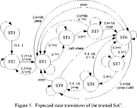
Based on the security attributes of the chip, together with control parameters and state flags, the state transitions of the dedicated secure SoC in the absence of errors is illustrated in Figure 5, where S.n denotes the nth bit of STATE, and O.n denotes the nth bit of OTP. As usual, we use value 1 to denote that the relevant condition can be satisfied, and use value 0 to denote the opposite situation.
When the chip begins operation, it is required to start at a certain secure state. The transitions between different states must satisfy some constraint conditions, which are organized according to relevant security attributes, and finally it is implemented by assigning different values to counterpart control parameters and state flags. For the sake of conciseness, in this subsection we firstly introduce the detailed constraint conditions of two complex state transitions as follows:
-
• State transition from ST1 to ST2, following constraint conditions should be satisfied.
DATA_T = TDESDEC(KEY_TDES, TDESENC (KEY_TDES, DATA_T))
DATA_R = RSADEC(PRIVATE_EK, RSAENC (PUB_EK, DATA_R))
PCR0 = SHA1(BOOTLOAD)
PCR1 = SHA1(DATAlevel0)
DIR0 = SHA1(PCR0 || PCR1)
M_AUTH = RSADEC(M_PUBKEY, M)
Notice that FENC(KEY, DATA) denotes encryption process using algorithm F, where DATA is the plain-text and KEY is the secret key. FDEC(KEY, DATA) denotes decryption process using algorithm F, where DATA is the cipher-text and KEY is the secret key. DATA_T, DATA_R and KEY_TDES are the random numbers generated by random number generation of the chip. PRIVATE_EK and PUB_EK are the public key and private key of EK respectively.
To fulfill the transition, it needs to judge whether previous five constraint conditions are satisfied or not. If not, OTP.4 is set and the chip is locked which means it do not work unless reboot. If satisfied, after receiving the security authentication command, it needs to judge whether the sixth formula is satisfied or not. If so, OTP.1 is set and the chip waits for the command of owner establishment. If not, OTP.6 is set and the chip is locked.
-
• State transition from ST3 to ST6 to ST9, following constraint conditions should be satisfied.
DATA_T = TDESDEC(KEY_TDES, TDESENC (KEY_TDES, DATA_T))
DATA_R = RSADEC(PRIVATE_EK, RSAENC (PUB_EK, DATA_R))
USER_AUTH = RSADEC(AIK_PUBKEY, M)
PCR0 = SHA1(BOOTLOAD)
PCR1 = SHA1(DATAlevel0)
DIR0 = SHA1(PCR0 || PCR1)
PCR2 = SHA1(COS)
PCR4 = SHA1(DATAlevel1)
DIR1 = SHA1(DIR0 || PCR2 || PCR4)
PCR3 = SHA1(APPLI)
PCR5 = SHA1(DATAlevel2)
DIR3 = SHA1(DIR0 || DIR1 || PCR3 || PCR5)
When the chip starts at state ST3 normally, it begins to validate the integrity of level 1 code and data, level 2
code and data. Then, after setting STATE.6, it enters ST6 by jump instruction. By judging whether STATE.4 is valid or not, it determines to enter ST9 or not. It can enter ST9 from ST6 using call instruction, and returns ST6 after called code execution using return instruction.
As to other simple state transitions, we shall not give their details here, and just list their constraint conditions briefly as follows:
-
• State transition from ST2 to ST3.
If the chip initializes, following condition should be satisfied.
M_AUTH = RSADEC(M_PUBKEY, M)
Else if the chip starts in its lifecycle, following condition should be satisfied.
USER_AUTH = RSADEC(AIK_PUBKEY, M)
-
• State transition from ST3 to ST4.
USER_AUTH = RSADEC(AIK_PUBKEY, M)
-
• State transition from ST4 to ST5.
The integrity measurement value stored in PCR2 should be equal to the incoming integrity value of level l code.
-
• State transition from ST5 to ST6.
No special condition needed.
-
• State transition from ST6 to ST7.
USER_AUTH = RSADEC(AIK_PUBKEY, M)
-
• State transition from ST7 to ST8.
The integrity measurement value stored in PCR3 should be equal to the incoming integrity value of level 2 code.
-
• State transition from ST8 to ST9.
No special condition needed.
-
• State transition from ST3 to ST2.
USER_AUTH = RSADEC(AIK_PUBKEY, M).
-
IV. TRUSTED MEASUREMENT AND TRANSFER STRATEGY
In the premise of trusting chip manufacturer, there have potential safety hazard when chip is carried from manufacturer to developer[5,6]. In order to resist the security threat, a share identity authentication key and a corresponding authentication protocol is set, only the developer who pass the identity authentication and authorization can obtain the access and trusted root to the corresponding chip, and establish its own application system and security mechanism and strategy for chip to accomplish the trusted measurement and trusted transfer in each chip application tache, and provide relevant cryptograph service for external environment.
-
A. Reliability measurement of application environment
When system startup normally and satisfy relevant security mechanism, system allow download COS into chip under the control of bottom system independent lead program. Once COS is downloaded and stored in system state control program storage zone, startup COS software integrality measurement program, do hash operation for COS, and compare with the received COS integrality measurement value DIRS, if they are equal, it indicate that incept COS correctly, and store the integrality measurement value into storage zone DIR register group which controlled by initial state, meanwhile, set COS operation allowance sign bit. Temporality, do hash operation for all function component data sequence in chip, and obtain the integrality measurement value PCRS before chip system operate COS, and then store it into PCR register group. Otherwise, forbid operating COS, set COS download fault state bit, and record the current operation executor, time, error type and so on for audit afterwards. COS download atomy control mechanism should be started during download process in order to avoid download process interruption caused by power cut off suddenly, swap and so on, and avoid operating incomplete COS program result in carrying chip system into unpredictable state and cause new security threat.
The download of application is accomplished under the COS control, the demand of download process, integrality measurement and download atomic is the same as COS download, obtaining application and data integrality measurement value DIRA and function component integrality measurement value PCRA and store in storage zone PCR and DIR register groups controlled by COS.
-
B. Classification startup and trusted transfer
When COS and user application are download, chip realize trusted transfer by irreversible bottom to application layer gradually starting module. Classification startup mechanism is realized under the support of storage management module, cryptograph function module and security management module. After initial state startup, monitor system state startup and operated; after system state startup and operated, monitor user state startup and operated. Follows take the chip system startup from initial state to system state flow which is depicted in Fig. 6 for example, explaining its trusted root transfer.
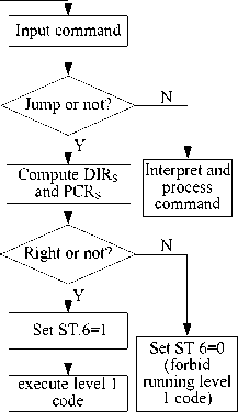
First, chip system do function self-test for arithmetic IP core under the lead and control of initial state and monitor software. If function self-test is failure, the chip system integral security depend on arithmetic IP core cryptograph function lost guarantee, setting function invalidation bit, and the chip is locked cannot execute any service. In the premise of correct function self-test, system do integrality measurement for parameters refer to PCRI and DIRI, and compare with the value stored in PCR and DIR register group. If integrality validation is correct, then entry into command wait state, otherwise, set function invalidation bit, and user can realize the jump from initial state to system state by level jump command. When chip systems receive level jump command, it does integrality measurement for system state COS program and corresponding state, and compare with the value stored in PCRS and DIRS. If pass the validation, chip system set system code enable sign bit, and allow system state code operation, and inherit the trusted and trusted root which pass the validation. Otherwise reset system code enable sign bit, and forbid COS code startup and operation.
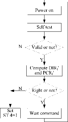
Figure 6. System startup flow from initial state to system state
Based on the above startup flow, by the integrality measurement and validation of function component state sequence, inner data and code, and combine with startup order regulation and trusted test, chip system can obtain system trusted root and trusted transfer. When initial data, code and function cannot pass the validity validation, it indicate that chip be in invalidation state, and chip turn into lock up state. When system state, user state data and code cannot pass integrality validation, it indicate that system state and user state be in unsecured state, and forbid chip enter into system state or user state code operation state, but allow chip enter into initial state in order to reconstruct and configure system state and user state and satisfy relevant security strategy and operation flexibility, to ensure the inheritance and transfer of trusted root.
-
C. System simulation and validation
-
V. Conclusion And future work
The trusted SoC chip we designed based on ETI 8051 is mainly applied in embedded cryptograph security equipment, as security service module, it provide identity authentication, key management and education and corresponding cryptograph service. Trusted SoC security architecture combined with COS can provide good cost performance, classification startup and trusted transfer mechanism insure the transfer of chip trusted root and the programs in chip all operate in corresponding trusted environment, it can provide some references for the design and application of SoC. And the further research will focus on the integrality measurement of dynamic data and environment in system operation.
The SoC industry was limited to pure hardware manufacturers. In the last ten years, this industry has given more and more importance to embedded software [10, 11]. Dedicated embedded software (e.g., embedded software for information security) has evolved according to conventional software engineering practices. Now, an application’s activity can be destroyed by a denial of malicious attack. Resource control becomes an important part of the security guarantees when untrustworthy software can be loaded over a trusted computing base. Consequently, our embedded software research now focuses on memory resource control and real-time hardware guarantees, which implies some specific constraints for the third-party code.
Acknowledgment
We are grateful to the reviewers and the editor that contributed to the great improvement of the original version of this paper with their valuable comments and suggestions.
References System Design of a Trusted SoC and Detailed Analysis of its Secure State Transitions
- C.-H. Anne , W. Thomas W. D. Shinder, et al.. Introduction to Information Security. The Best Damn Firewall Book Period, 2008, pp 3-52.
- J. Dong, K. Ackermann, C. Nita-Rotaru. “Secure group communication in wireless mesh networks”. Ad Hoc Networks, vol. 7, pp. 1563-1576, 2009.
- S. Mühlbach, S. Wallner. Secure communication in microcomputer bus systems for embedded devices. Journal of Systems Architecture, vol. 54, pp. 1065-1076, 2008.
- D. Feng, “Support platform and interface criterion of trusted computing cryptography technology,” Beijing, State password administration, 2007.(in Chinese)
- Trusted Computing Group, “TPM Main Part 1: Design Principles, Version 1.2, Revision 94,” http://www.trustedcomputinggroup.org/specs/TPM/Main Part1/Rev 94.zip, 2007.
- Trusted Computing Group, “TPM Main Part 2: TPM Structures, Version 1.2, Revision 94,” http://www.trustedcomputinggroup.org/specs/TPM/Main Part2/Rev 94.zip, 2007.
- Common Criteria for Information Techology Security Evaluation, Part 1: Introduction and general model, Version 2.3, August 2005. http://www.commoncriteriaportal.org/
- L. Zhang, L. Zheng, R. Wang, and S. Wen, “Desing and Implementation of Multiple Cryptographic Algorithm Interface Circuit Based on Secure SoC,” in Proceedings of International Conference on Wireless communications, Networking and Information Security, Beijing, 2010, pp. 510~514.
- F. Salewski. A. Taylor. “Fault handling in FPGAs and microcontrollers in safety critical embedded applications: a comparative survey”. In Proceedings of DSD 2007 10th Euromicro Conference on Digital System Design Architectures, Methods and Tools, August 29–31, 2007.
- F.Vahid. “It’s time to stop calling circuits ‘Hardware’. IEEE Computer, vol. 40, pp. 106-108, 2007.
- H. Mouratidis, P. Giorgini. Integrating Security and Software Engineering: Advances and Future Visions. Idea Group Publishing, 2006.
