Technical Study on Low Power VLSI methods

Author: T.Kapilachander, I.Hameem Shanavas, V.Venkataraman
Journal: International Journal of Information Engineering and Electronic Business(IJIEEB) @ijieeb
Article in issue: 1 vol.4, 2012.
Free access
In recent days every application must need power management. In this paper we presented a various techniques to handle the power management in IC. Power dissipation in a IC is base on power used by the IC and also by heat dissipation. To reduce energy use or to minimize heat dissipation some of the techniques are briefly discussed in this paper. Power management is becoming an increasingly urgent problem for almost every category of design and application, as power density, measured in watts per square millimeter, rises at an alarming rate. Power needs to be considered at the very early stages of a design, when the opportunity to save power is at a maximum. At the same time, making a design extremely power efficient results in trading off area and/or timing. For a Integrated Circuit (IC) perspective, effective energy management for a SoC (System-on-a-chip) must be built into the design starting at the architecture stage; and low-power techniques need to be employed at every stage of the design, from RTL (Register Transfer Level) to GDSII. This paper explains about the combination of techniques used for low power approach in integrated circuits (IC) or Chip
Logic restructuring, Clock tree and clock Gating, Transistor Sizing, Pin swapping, multi-threshold voltage, Dynamic voltage scaling, DVFS, power gating, Memory splitting, Substrate biasing
Short address: https://sciup.org/15013112
IDR: 15013112
Text of the scientific article Technical Study on Low Power VLSI methods
Power consumption is an important issue the semiconductor ecosystem is trying to address. It concerns electronic product providers across all
segments. For example the power consumption in the CMOS device is major concern with Static power , Dynamic power and Short Circuit Power. Mainly two components determine the power consumption in a CMOS circuit Static power consumption and Dynamic power consumption, since Short Circuit Power Consumption is rarely occurred one. So the total power consumption for the a CMOS device is given by
P
dissipation
= static
+P
dynamic
+P short circuit
– (1.2)
The power Consumption for a single CMOS is
approximately 5V. In VLSI fabrication billions of gate fabricated assume that how much power we needed to operate a single Chip. From this above analysis we know the awareness of power reeducation needed for the Integrated Circuits(IC).
Today, power and performance have become the predominant concerns for chip designers. Low power consumption is vital for handheld mobile and wireless devices as most of them are independent battery as the power source. Power management is becoming an increasingly urgent problem for almost every category of design, as power density (measured in watts per square millimeter) rises at an alarming rate. Fig. 1 shows an increase in the power density with shrinking device geometry
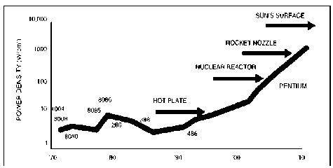
Fig.1.1 Power density with shrinking device
The static power dissipation is due to reverse saturation, sub-threshold and leakage current and occurs especially when the device is in idle mode. The dynamic power dissipation occurs due to charging and discharging of load capacitance and short-circuit current when both the NMOS and PMOS devices remain ‘on’ for a short time duration
P switching = afC eff V dd------ (1.2)
where ‘a’ is switching activity, ‘f’ is switching frequency, Ceff is effective capacitance and Vdd is supply voltage.
P short-circuit = I sc V dd f--------(1.3)
where Isc is short-circuit current during switching, Vdd is supply voltage and ‘f’ is switching frequency. Dynamic power can be lowered by reducing the switching activity and clock frequency, which affects performance, and also by reducing the capacitance and supply voltage. Leakage power is a function of supply voltage V dd , switching threshold voltage V th and the transistor size
P Leakage = f (V dd , V th , W/L) --------- (1.4)
where V dd is supply voltage, V th is threshold voltage, ‘W’ is transistor width and ‘L’ is transistor length
The performance of the IC is based on the circuit speed, In general, "small area" and "high performance" are two conflicting constraints. The IC designers' activities have been involved in trading off these constrain. Power dissipation issue was not design criterion but an afterthought. In fact, power considerations have been the Ultimate design criteria in special portable applications such as wrist watches and pacemakers for a long time. The objective in these applications was minimum power for maximum battery life time.
There are so many numbers of ways to over come this power consumption problem. In this further section of paper deals with the possible techniques available for the power management in an IC for long battery life .
-
2 . Methods of Power Management
-
2.1 Logic restructuring
-
2.2 Clock tree optimization and clock Gating
Due to the impressive advancement of the VLSI circuit technology has been the rapid scaling down the feature size, i.e., the minimum dimension of the transistor. It decreased from 2µm in 1985 to 0.35µm in 1996. According to the National Technology Roadmap for Semiconductors (NTRS) it will further decrease at the rate of 0.7µm X per generation (consistent with
Moore’s Law) to reach 0.07µm by 2010. Such rapid scaling has two profound impacts. First, it enables much higher degree of on-chip integration. The number of transistors per chip will increase by more than 2x per generation to reach 800 millions in the 0.07µm technology. Second, it implies that the circuit performance will be increasingly determined by the interconnect performance. The interconnect design will play the most critical role in achieving the projected clock frequencies.[11] Interconnect has become the dominating factor in determining circuit performance and reliability in deep submicron designs interconnect design as the technology feature size rapidly decreases towards below 0.1 micron. Thus we need a commonly used interconnect models and a set of interconnect design and optimization techniques for improving interconnect performance and reliability.[18]
-
2.3 Logic resizing (transistor resizing)
Due to the increased circuit density and speed, the power dissipation has emerged as an important consideration in circuit design. A lot of efforts on power reduction have been made at various levels of design abstraction. Considering the fact that the charging/discharging of capacitance is the most significant source of power dissipation in well-designed CMOS circuits
Power consumption grows exponentially at 90nm and beyond technologies. At smaller geometries, aggressive management of leakage current can greatly impact design and implementation choices. Indeed, for some designs and libraries, leakage current exceeds switching currents, thus becoming the primary source of power dissipation in CMOS Depending upon the architecture of the design, the designers can choose from a wide range of options for reduction in power consumption of VLSI circuits. Some of the techniques to reduce the power consumption are briefed below.
There are several methodology are available for low power management for IC. Some of them are listed below and briefly discussed ( 1) Logic restructuring (2) Clock tree optimization and clock Gating (3) Logic resizing (transistor resizing). (4) Transition rate buffering. (5) Pin swapping (6) Using multi-threshold voltage (7) Multi-supply voltage (voltage islands) (8) Dynamic voltage scaling (9) Dynamic voltage and frequency scaling (DVFS) (10) Power shutoff or power gating (11) Memory splitting (12) Substrate biasing (body-biasing or back-biasing) (13) Operand isolation
The CMOS design uses both NMOS and PMOS transistors for logic design. Due to mobility variation in NMOS and PMOS transistors, the rise and fall time differ. By moving high switching operations up in the logic cone and low switching operations back in the logic cone, a considerable amount of power can be saved[5][16]
Clock distribution is crucial for timing and design convergence in high-performance very large scale integration designs. Minimum-delay/power zero skew buffer insertion/sizing and wire-sizing problems have long been considered intractable .Most of the power is consumed due to the high clock frequency used for operating the device. Portions of the clock tree that are not being used at any particular time can be disabled to save the power.
The length-to-width ratio of transistors determines the driving strength and speed. Upsizing improves slew times, reducing dynamic current. Hence The dynamic power consumption is reduced. Downsizing reduces leakage current, thereby reducing the static power consumption. To be effective, sizing operations must include accurate switching information.[2][8] Gate Sizing (GS) is a well-known technique which targets power optimization by reducing load capacitance several approaches have been published from a general point of view, reducing the physical size of a gate, at logic level, leads to the gate delay increase which implies the decreased slack time. The basic rule is to use the smallest transistor or gates that satisfied the delay constraints. To reduce the dynamic power the gate that toggle with higher frequency should be made smaller. Actually the basic rule sounds simple, the actual sizing problem is very complicated [6][7]. Consider a part of the circuit part as shown in the below figure 2.1. Suppose that the gates are not on the critical delay path and should be size down. We can size down the first gate, the second gate, or both, subjected to the available sizes in the cell library as long as the path delay is not violated[12]. If the path contains many gates, the optimization problem quickly becomes very complicated.
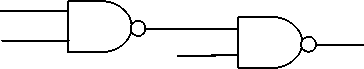
Fig. 2.1. Model circuit
The concept of slack time is often used to express the timing constrains of the circuit. The slack time of a gate is the difference between the signal required time and the signal arrival time at the output of the gate. A positive slack time means that the signal arrived earlier than its required time and the gate can be sized down. The goal of gate sizing is to adjust the gate sizes such that the slack time of each gate is s low as possible without any gate having a negative slack i.e., time violation a greedy algorithm was proposed by an exact algorithm for low power library specification gate resizing, it attempts to downsize a set of gates that gives the most reduction in the power dissipation without affecting the time slack of all other gates. The new slack times of the downsized gates are then compute and a new set of gates is selected.
The simplest transistor gate sizing problem is that of an inverter chain the general design problem is to derive a large capacitive load without excessive delay, area and power requirements. In a chain of successively large inverter, so that all the inverters in the chain drive appropriate loads and do not causes excessive delay. Using a simple RC delay model in inverter chain the delay of the inverter is directly proportional to the load it drives. For example if an inverter drives K other inverters of the same size, the delay through the inverter is Kd where d is the intrinsic delay of the inverter under a single load. Then the total delay is given by D through the chain.
D = NKd
D= ln(C N /C 0 )(K/lnK)d (2.3.1)
-
2.4 Transition rate buffering
-
2.5 Pin swapping
Timing optimization techniques for VLSI circuits have received much attention in recent years due to increasingly aggressive designs and technology trends Such as shrinking geometry. Thus the timing optimizations focus on buffer insertion that is buffering of transistor.
Buffer insertion is a powerful technique largely because of the decoupling property of buffers. Most of the previous research on buffer insertion or otherwise call it as a fan-out optimization to reduce the power consumption of the particular device or circuit. Buffer insertion is used to minimize the slew rate. The main thing to reduce the slew rate by Optimal polynomial-time algorithms for the minimum Power consumption by buffer insertion problems[23], computation of the entire power-delay curve and an efficient slew rate minimization to obtain sub-optimal solutions
Due to the finite delays of logic gates, signal races in static logic deigns can result in dynamic hazards. Hence, a node can have transitions in one clock cycle before stabbing to the correct Logic level. These unnecessary switching transitions (glitches) can consume power dissipation in the order of 20-40% to reduce this power the first approach is to balance the path delays by changing the logic structure. Another technique is to balance the delay of the paths by sizing down the gates in the fast paths; however, this approach can increase the delay of the circuit. Also insertion of buffers (delay elements) in the fast paths can balance the delay. However, the addition of more numbers of buffers increase the power dissipation.
Some cells can have input pins that are symmetric with respect to the logic function (for example, in a 2-input NAND gate the two input pins are symmetric), but have different capacitance values. Power can be reduced by assigning a higher switching rate net to a lower capacitance pin
Power minimization techniques are re-factoring, remapping, phase assignment and pin swapping. All these techniques can be classified as local transformations[20]. They are applied on gate netlists, and focus on nets with large switched capacitance. Most of these techniques replace a gate, or a small group of gates, around the target net, in an effort to reduce capacitance and switching activity. Similarly to resizing, local transformations must carefully balance short circuit and output power consumption[31][32]
For example take a 4 input NAND gate with different capacitance value at the pin as show in the Fig.2.5.1
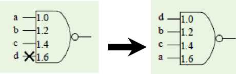
In this above example among this four pin in NAND gate pin swapping is applied in this example a high activity net is connected to the pin no 4 that is pin “d” which has the minimum input capacitance. To achieve the minimum input capacitance pin swapping is done between the pins “a” and “d”.
-
2.6 Using multi-threshold voltage
-
2.7 Multi-supply voltage (voltage islands)
Advanced CMOS technology can also allow very low power operation of battery powered handheld devices by scaling down the supply and device threshold voltages (Vt) to a level which just maintains acceptable performance for a several application. This method achieves low active power, but comes at a cost of increased standby power resulting from increased device leakage power[4][14].
Multi-threshold CMOS (MTCMOS)has been described as a method to reduce standby leakage current in the circuit, with the use of a high threshold apply to the MOS device to de-couple the logic either from the supply or ground during long idle periods, or sleep states. The Figure 2.6.1 shows a MTCMOS [Multi Threshold Voltage Complementary Metal Oxide
Semi Conductor] circuit, where the logic block is constructed using low threshold devices and the Power supply given to the gate of the of the MTCOMS is a high threshold header switch, or the ground terminal is gated by a high threshold footer switch[10].
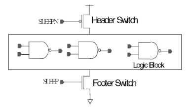
Fig. 2.6.1. MTCMOS circuit
During active operation of the MTCMOS circuit described by the above Figure the power interrupt switch is turned on by the SLEEPN (or SLEEP) signal and current dissipated by the logic is drawn through the interrupt switch which causes a reduction in drive voltage seen by the logic, reducing logic performance. To compensate for the reduction in logic performance: larger power supply voltages can be used to at the expense of increased active power for similar performance, larger device widths for the power interrupt switch can be used to minimize performance impact, at the expense of increased area and power for entering and existing sleep mode, and adjustments in device implants to allow moderately high threshold values is another technique that can be used to increase performance of the device during idle mode.
Multi-Vdd is an effective method to reduce both leakage and dynamic power, by assigning different supply voltages to cells according to their timing criticality. In a multi-Vdd design, cells of different supply voltage are often grouped into small number of voltage islands (each having a single supply voltage), in order to avoid complex power supply system and excessive amount of level shifters. Low power design methodology which manages power, timing and design cost by using multi-Vdd and voltage islands has to be developed[9][10]. This can be done by presenting an algorithm that in a multi-Vdd design with cells assigned different supply voltage One prerequisite of the voltage island grouping algorithm, is an initial voltage assignment at the standard cell level that meets timing and then to find method to produce an initial voltage assignment which not only meets timing but also good proximity of high voltage cells to provide the voltage island grouping algorithm with a smooth input. Sometimes a few isolated critical cells (called outlier) may still exist in the resulting voltage assignment, causing disproportionately expensive penalty to the final voltage island grouping. Finally improve the voltage assignment by automatic outlier detection followed by incremental placement.
-
2.8 Dynamic Voltage Scaling
-
2.9 Dynamic Voltage and Frequency Scaling
Dynamic voltage scaling (DVS) is a standard technique for managing the power consumption of a system. It is based on the fact that the dynamic (switching) power P of CMOS circuits is strongly dependent on the core voltage V and the clock frequency f according to
P α f v 2 ------(2.8.1)
Under the assumption that the number of clock cycles required for a computation is independent of the core frequency, the execution time is inversely proportional to the frequency. The total energy E for the computation is then proportional to the square of the voltage:
E α v 2 ------ (2.8.2)
Note that the total energy for a computation is not depend on the frequency, but a reduced core voltage requires a reduction of the clock frequency and therefore implies a longer overall execution time. The assumptions behind Equation (2.8.2) are highly uncertain as they ignore other system components in particular the bus and memory. The other components impact the execution time of a program leading to a much more complex dependence on the processor frequency[13].
Dynamic Voltage and Frequency Scaling allows a host to dynamically switch its CPU frequency dependent on its load requirement. It do this by continuously monitoring the CPU utilization with the DVFS algorithm determining any necessary adjusts to the CPU’s frequency with the goal being to run the
CPU at a lower frequency so that it consumes less power. It uses processor performance states (P-states) presented to the VM kernel through an ACPI interface to achieve this. For example: If your 2GHz CPU is sitting at 30% utilization then DVFS will reduce the frequency of the CPU so it will operate nearer to its 600MHz frequency requirement including enough headroom to accommodate a sudden increase in CPU requirement[3][13][27][28].
-
2.10 Power shutoff or power gating
Power Gating is effective for reducing leakage power. Power gating is the technique in circuit temporarily turned off the sub blocks to reduce the overall leakage power of the chip. This temporary shutdown time can also call as "low power mode" or "inactive mode". When circuit blocks are required for operation once again they are activated to "active mode". These two modes are switched at the appropriate time and in the suitable manner to maximize power performance while minimizing impact to performance. Thus goal of power gating is to minimize leakage power by temporarily cutting power off to selective blocks that are not required in that mode. Power gating affects design architecture more compared to the clock gating. It increases time delays as power gated modes have to be safely entered and exited. The possible amount of leakage power saving in such low power mode and the energy dissipation to enter and exit such mode introduces some architectural trade-offs. Shutting down the blocks can be accomplished either by software or hardware. Driver software can schedule the power down operations. Hardware timers can be utilized. A dedicated power management controller is the other option.
An externally switched power supply is very basic form of power gating to achieve long term leakage power reduction. To shutoff the block for small interval of time internal power gating is suitable. Power gating uses low-leakage PMOS transistors as header switches to shut off power supplies to parts of a design in standby or sleep mode. NMOS footer switches can also be used as sleep transistors. Inserting the sleep transistors splits the chip's power network into a permanent power network connected to the power supply and a virtual power network that drives the cells and can be turned off.
The quality of this complex power network is critical to the success of a power-gating design. Two of the most critical parameters are the IR-drop and the penalties in silicon area and routing resources. Power gating can be implemented using cell- or cluster-based approaches or a distributed coarse-grained approach.
Power-gating parameters Power gating implementation has additional considerations than the normal timing closure implementation. The following parameters need to be considered and their values carefully chosen for a successful implementation of this methodology .
-
• Power gate size
-
• Gate control slew rate:
-
• Simultaneous switching capacitance
-
• Power gate leakage
-
2.11 Memory Splitting
-
2.12 Substrate Biasing
-
2.13 Operand Isolation
Off-chip memory accesses are very expensive power wise, studying the reordering of bus transactions (to minimize signal transitions) reduce overall energy consumption. One strategy for reducing the number of bit flips on the memory bus is to schedule bus transactions (we consider a bus transaction to be a read or write of a single word) in the order in which they would cause the minimal signal changes. For example, a load that follows a stored program execution in order cannot be scheduled before storeing (assuming they use the same address) Likewise, an instruction that causes a data cache line replacement must be scheduled before the transactions that replace the line. To investigate the effect of reordering bus transactions on energy consumption, we incorporated a transaction scheduler. The scheduler maintains a list of recently seen off-chip memory access events and schedules bus transactions from the list according to which transaction causes the least bit flips given the current state of the bus. The scheduler ensures that all dependences between instructions and memory reads and writes are satisfied by building the dependence graph and only scheduling transactions that are leaf nodes[33]. The transaction scheduler uses priority list scheduling, where the priority is the number of bit transitions between successive bus transactions. The scheduler accepts an input event from a memory access trace, and places it in the scheduling list. If the new event causes the list to reach a threshold size, an event is removed from the list and scheduled as a bus transaction. Only those events that are have no dependences with other events in the list may be scheduled as an output transaction. Of the ready events, the one that causes the least number of signal transitions is chosen[15]. The scheduler is locally greedy and may not find an optimal order for the whole trace. However, with large thresholds, the scheduler gives a good approximation that indicates the worth of reordering transactions.
Silicon-on-Insulator (SOI and SOS included) CMOS technology has been a choice for radiation tolerant electronics. This technology has clear advantages over bulk CMOS in removing the mechanism for latch-up and in having smaller single events upset (SEU) cross section. However, the total ionization dose (TID) effect is usually of a concern. This is because that SOI device has back channel leakage that is usually only controlled through special fabrication process. In addition to the back channel, there is edge leakage that is common to bulk CMOS and is usually mitigated through special layout techniques. With the decreasing feature size and the substrate thickness, TID effect may be of less a concern, especially in applications where the dose rate is moderate and when the radiation induced leakage current during high dose rate test can anneal away in room temperature in a proper period of time calculated according to the realistic dose rate in the actual application. However, in applications where high dose rate (> 1 k rad/hr) is present, like in some high energy physics experiments, back channel leakage is still an issue It has been observed that the biasing condition on the gate of a transistor during irradiation affects the changes of threshold voltage and leakage current caused by the total dose. This is because that this bias voltage generates an electrical potential inside the gate oxide and that potential affects the transportation of hole-electron pairs generated by radiation which in turn affects the final trapped charges inside this gate oxide. The polarity and amount of the trapped charge are responsible for the radiation induced leakage current and for the threshold voltage change. With thin substrate, conductive back plate placed under or deposited on the substrate were used to provide bias and form a “back gate” after the irradiation to understand the mechanism of radiation induced back channel leakage and to mitigate the leakage increase by applying a bias toback gate . In reference with a 150 micron sapphire substrate, 200 V bias has to be applied to the back plate in order to shift the I-V curve back to its pre-irradiation condition. In reference Transistors fabricated using 0.15 micron SOI technology with buried oxide on silicon substrate are subjected to irradiation of a 70 MeV proton beam. Both leakage current increase and threshold voltage shift are observed in NMOS and in PMOS. Back gate bias is applied after the irradiation to move the I-V curve back to the pre-irradiation condition. The optimum value of the back gate voltage for both NMOS and PMOS is found to be -23 V. I propose here a mechanism that is different from this back gate theory. I believe that by providing electrical potential in the substrate during irradiation when radiation induced hole-electron pairs are generated, transported, recombined and a few trapped, it is possible to affect the trapped charges in the substrate so as to control the leakage increase. In the back gate mechanism, because of the rather thick back gate insulation (the substrate thickness of a few hundreds of micro-meters comparing with the front gate oxide thickness of a few to a few tens of nano-meters), the required back gate bias is usually rather high to move the I-V curve after the irradiation. In the mechanism I propose, because it relies on guiding the transportation of different charges when they are generated inside the substrate, the required bias should be much smaller than that in the back gate case. Take SOS CMOS as an example, radiation induced leakage current has been reported in NMOS, PMOS and in both transistors during irradiation tests at different dose rate and total dose. We know that trapped positive charge is responsible for leakage current in NMOS, while trapped negative charge is responsible for leakage in PMOS. If a bias is applied through the back plate to the substrate, positive bias will attract electrons towards the back plate leaving a higher positive charge density in part of the sapphire substrate that is close to the silicon-sapphire interface, hence causing leakage increase in NMOS and suppressing leakage in PMOS. When the bias voltage is negative, electrons are pushed toward the silicon-sapphire interface and that creates a higher negative charge density near the interface to cause leakage increase in PMOS while suppress the leakage in NMOS. An optimum bias voltage (constant or as a function of accumulated dose) may exist to have the minimum change in leakage and threshold voltage in both NMOS and PMOS. Tests have been carried out on one particular type of SOS device that is commercially available and the above predictions in leakage (or the lack of it) in NMOS and PMOS are confirmed. A constant optimum bias voltage for both NMOS and PMOS has been found to be only a few volts. Experiments are to be carried out to study this mechanism and its predictions on other types of SOI devices.
The idea of operand isolation is to identify redundant operations and, using special isolation circuitry, prevent switching activity from propagating into a module whenever it is about to perform a redundant operation. Therefore, the transition activity of the internal nodes of the module and, to a certain extent, its transitive fanout is reduced significantly, resulting in lower power consumption . To illustrate the concept of operand isolation, let us consider a small example. Figure 1 shows a part of a design in which the result of an operation performed by adder a0 is evaluated conditionally in its transitive fanout. For certain configurations of the multiplexor select signals S0_S1, and S2 and the register load enable signals G0 and G1, the output of a0 is not used to compute the values to be stored in registers r0 and r1. However, a0 will continue to compute a new output whenever there is switching activity at its inputs A and B, therefore consuming power by executing redundant computations. For long periods in which the output is not used, this power overhead can be substantial.
5b
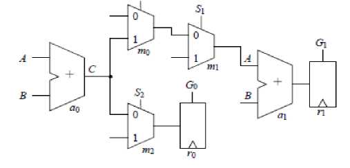
-
Fig.5. Design without operand isolation.
Suppose now that there is an activation signal ASa 0 whose logic value indicates if a 0 performs a computation 1that is not redundant. We can use ASa 0 to control blocking logic, e.g. transparent latches that “freeze” the inputs of a 0, effectively preventing the propagation of switching activity into the module. The module will therefore only perform non-redundant computations. The lower transition probability at the internal nodes of the module will then result in lower power consumption. Figure 2 shows the same circuit where the inputs of the two adders have been isolated using latches. Assuming that ASa 0 evaluates logic ‘0’ whenever a 0 is performing a redundant computation, inputs A _ and B _ maintain their previous values and do not transition when the operation to be performed by a 0 is redundant.
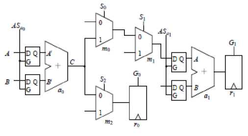
Fig.6. Design with operand isolation.
An algorithm to automate the application of operand isolation to a given RTL circuit will have to solve the following two key problems: Select a set of modules for which operand isolation results in the largest reduction in power consumption for the overall circuit, and for each of these modules, obtain an activation signal which indicates that the module is performing a computation that is not redundant.
-
3 Conclusions:
High power consumption not only leads to short battery life for hand-held devices but also causes on-chip thermal and reliability problems in general. As application demands increase toward more power sensitive devices, new and novel approaches are needed to meet those demands. The techniques discussed in this paper can help the SoC designer to meet those goals. Several of these techniques can be used in unison to provide the lowest power solution possible. Sleep mode, clock gating, power gating, gate level optimizations, low power libraries, low power architectures and voltage scaling are all proven low power techniques and should be considered when architecting any new application. It is important to partner with a silicon vendor that has the extensive experience, expertise and IP portfolio required to successfully design and manufacture ultra low power devices.
References Technical Study on Low Power VLSI methods
- Transistor and pin reordering for gate oxide leakage reduction in dual circuit
- J.Kaoetal “Transistor sizing issues and tool for multi threshold CMOS technology” in proceedings of ACM/IEEE DAC pp.409-414,JUN 1997
- QqiangMQ & Evangeline “Voltage island – Driven floor planning” in proceeding of IEEE pp644-649 2007
- Stephen, Mike, Hook “Enhanced multi threshold (MTCMOS) circuit usinh variable well bias” in ISPED’01/ACM pp165-169 August 2001
- Chang, Cheng “Post layout logic restructuring using alternative wires” in Proceedings of IEEE pp587-596 August 1996.
- W.Chen, C.T Hsieh, M.Pedram “Gate sizing with controlled Displacement” in Proceedings of international symposium on physical design pp127-132 1999
- O.Coudert, R.Haddad, “New algorithm for gate sizing comparative study” in proceedings of 33rd Design Automation Confrence pp734-789 Jun 1996
- M.Hashimoto, HiOnodera & K.Tumara “A practical gate resizing technique considering glitch reduction for low power desing” in proceedings of Design Automation Conference 1999
- J.M.Cheng & M.Pedram “Energy minimization usig multi supply voltage” IEEE Transaction on VLSI System Vol 5: no: 4 pp 1- 8 December 1992
- C.Chen & M.Sarrafzadeh “ A Efficient algorithm for gatelevel power delay trade of using two voltages” International conference on computer Design pp222-227 October 1999
- Qing Wu, M.Pedram & Xunwei “ Clock gating and its application to low power design of sequential circuits” in IEEE Transction pp415-420 in Vol-47 no103 March 2000
- Oliver Coudert, “Gate Sizing for Constrained delay/power/area optimization” in IEEE Transcation on VLSI Design September 1997
- P.J.Shah, P.Patil, V.M.Deshmukh & P.H.Zope. “ Low Power VLSI Design using Dynamic Thershold logic” in proceedings of SPIT – IEEE Colloquium international Conference Mumbai Vol-2.121
- S.I.Mutuh, T.Douseki, “ I-V power supply high speed digital circuit technology with multi threshold voltage CMOS” in IEEE Journel of solid state circuits Vol-30 August 1995
- D.E.Lackey, Paul.S, Zuchuwski.T.rBedmur, “Managing power and performance for system on chip Design using voltage island
- Kai Chang Wu, Diana Marculescu,”Joint logic restructuring and pin reordering against NBTI-induced performance degradation”. Proceedings of the Conference on Design, Automation and Test in Europe European Design and Automation Association 3001 Leuven, Belgium, ©2009 ,ISBN: 978-3-9810801-5-5
- Roy K., Prasad S.C., “Circuit activity based logic synthesis for low power reliable operations,” IEEE Transactions on Very Large Scale Integration (VLSI) Systems”, Volume 1, Issue 4, Dec. 1993, pp 503 – 513
- Monica Donno, Alessandro Ivaldi, Luca Benini, Enrico Macii,” Clock-tree power optimization based on RTL clock-gating”, Proceedings of the 40th annual Design Automation , ACM New York, NY, USA ©2003, ISBN:1-58113-688-9
- Weixiang Shen; Yici Cai; Xianlong Hong; Jiang Hu; “An Effective Gated Clock Tree Design Based on Activity and Register Aware Placement” , IEEE Transactions on Very Large Scale Integration (VLSI) Systems, Volume: 18 Issue:12, page(s): 1639 - 1648 ISSN: 1063-8210
- Seongmoo Heo and Krste Asanovi´ c “Dynamically Resizable Static CMOS Logic for Fine-Grain Leakage Reduction”, MIT CSAIL Technical Report (MIT-LCS-TR-957), July 2004.
- A. Khan, P. Watson, G. Kuo et all. “A 90nm Power Optimization Methodology and its’ Application to the ARM1136JF-S Microprocessor”, 2005 IEEE Custom Integrated Circuits Conference, San Jose, CA.September 21, 2005
- Le, H.-B. Do, X.-D. Lee, S.-G.” Compact low-power high-slew-rate buffer for LCD driver application”,IEEE Electronics Letters ,Volume: 46 Issue: 20 ,On page(s): 1370 - 1371 ISSN: 0013-5194
- Yanbin Jiang; Sapatnekar, S.S.; Bamji, C.; Juho Kim; “Interleaving buffer insertion and transistor sizing into a single optimization” IEEE Transactions on Very Large Scale Integration (VLSI) Systems, Volume: 6 Issue:4 On page(s): 625 - 633 ISSN: 1063-8210
- Ronald J. Landry, “Low power microcontroller design techniques for mixed-signal applications”, AMI Semiconductor, Inc.Dallas, Texas USA,Industry Article.
- Pilar Parra, Antonio Acosta, and Manuel Valencia,” Reduction of Switching Noise in Digital CMOS Circuits by Pin Swapping of Library Cells” , Proceedings of PATMOS conference , 2001.
- Behnam Amelifard,” Low-power fanout optimization using multiple threshold voltage inverters” , Proc. ISLPED , 2005.
- Wong, M.D.F,” Low power design with multi-Vdd and voltage islands”, ASIC, 2007. ASICON '07. 7th International Conference on Issue Date: 22-25 Oct. 2007 On page(s): 1325 - 1325
- Li Shang Li-Shiuan Peh Niraj K. Jha,” Dynamic Voltage Scaling with Links for Power Optimization of Interconnection Networks”, The Ninth International Symposium on High-Performance Computer Architecture, 2003. HPCA-9 2003. Proceedings. Issue Date: 12 Feb. 2003 On page(s): 91 - 102 ISSN: 1530-0897
- Chung-hsing Hsu, Ulrich Kremer “Dynamic Voltage and Frequency Scaling for Scientific Applications “,Proceedings of the 14th annual workshop on Languages and Compilers for Parallel Computing , 2001
- Shi-Hao Chen; Jiing-Yuan Lin;” Implementation and verification practices of DVFS and power gating “,International Symposium onVLSI Design, Automation and Test, 2009. VLSI-DAT '09. Issue Date: 28-30 April 2009 On page(s): 19 - 22 Print ISBN: 978-1-4244-2781-9
- S. Heo and K. Asanovic. “Leakage-biased domino circuitsfor dynamic fine-grain leakage reduction”. Int Symp. on VLSI Circuits, pages 316–319, 2002.
- S. Narendra et al. ,”Scaling of stack effect and its application for leakage reduction”. In ISLPED, pages 195–200, Augu 2001.
- Y. Ye, S. Borkar, and V. De. ,”A technique for standby leakage eduction in high-performance circuits,”. In Symp. on VLSICircuits, pages 40–41, 1998
- Kessler, I.; Sidi, M.;” Splitting algorithms in noisy channels with memory”, INFOCOM '89. Proceedings of the Eighth Annual Joint Conference of the IEEE Computer and Communications Societies. Technology: Emerging or Converging, IEEE Digital Object Identifier: 10.1109/INFCOM.1989.101446 Publication Year: 1989 , Page(s): 136 - 142 vol.1
