The influence of mobile positive charge on electronic conductivity of dielectric with heterogeneous blocking border

Author: Perov G.V., Sedinin V.I.
Journal: Сибирский аэрокосмический журнал @vestnik-sibsau
Section: Математика, механика, информатика
Article in issue: 5 (26), 2009.
Free access
The correlation between the size of a positive mobile charge and electronic conductivity of oxide on polycrystalline silicon is established with the help of experimental method of thermally stimulated polarization and depolarization of MIS-structures. The boundary conditions of a problem for the working model of behavior of a mobile charge in isolating layers generated on a rough semiconductor film are formulated.
Mobile charge of a dielectric, heterogeneous blocking border between a dielectric and a semiconductor, oxide on polycrystalline silicon
Short address: https://sciup.org/148176108
IDR: 148176108
Text of the scientific article The influence of mobile positive charge on electronic conductivity of dielectric with heterogeneous blocking border
Multilayer components consisting of semiconductor, dielectric, conductor layers are the basis of modern microelectronic structures. The technology of formation of these layers develops permanently in the direction of improvement of reproducibility of electric parameters and physicochemical properties. One of the basic technological problems is conductivity control in the dielectric films which are built into active electronic blocks both on a plane surface of a single-crystal substrate and on a surface of granular layers, for example, of polycrystalline silicon.
Conductivity of various dielectric layers including layers formed on rough surfaces is well studied. The influence of separate components of a charge on conductivity of isolating films is the goal of permanent researches. For example, the influence of a negative charge of electrons trapped in the film of oxide over polycrystalline silicon (OPs) on its conductivity is considered in details in [1; 2]. The influence of a surface charge consists in shielding of external electric field by this charge and is accompanied with decreasing of conductivity of an oxide layer. However, until recently there are no data about the influence of a positive ionic charge, mobile under thermo-field loadings on electric conductance of dielectric films with heterogeneous blocking border. The results of researches of this problem are presented in this paper.
For this investigation the complex of techniques including measurements of volt-ampere characteristic (VAC) of samples ataroom temperature, currents TSP/TSD of test structures within temperature range of 30...300 °C was used. The conductivity of a dielectric layer was estimated by the size of electric field of breakdown dis, corresponding to the density of current through structure 10–6 /cm2. The general density of mobile ions N mc in oxide was defined by the area of curves of TSP/TSD currents.
Measurements were taken on a series of the samples prepared by thermal oxidation of polycrystalline silicon (OPs).
Presence of ions in OPs causes movement of VAC of dielectric in the region of smaller electric fields in a wide range of density of currents from 10–6 /cm2 till 10–10 /cm2 and changes the slope of VAC (fig. 1). This movement of VAC decreases from maximum level in a low-voltage part of a curve to a minimum level in a low-voltage part. So, for a pair of samples with density of a mobile charge 4∙1011 cm–2 and 4∙1012 cm–2 the movement of VAC is 1 MV/cm and 0,2 MV/cm undercurrentdensityof10–10 /cm2 ( <2MV/cm) and10–6 /cm2 (> 4 MV/cm) respectively.
Under the increasing of ions concentration Nmc in OPs, the dielectric strength disofoxidefilmsonPsmonotonously decreases, whereas the conductivity of structure increases (fig. 2). So, if the concentration of ions in a dielectric increases by a factor of a hundred, the electric field of disruption OPs decreases by a factor of 1.5 .
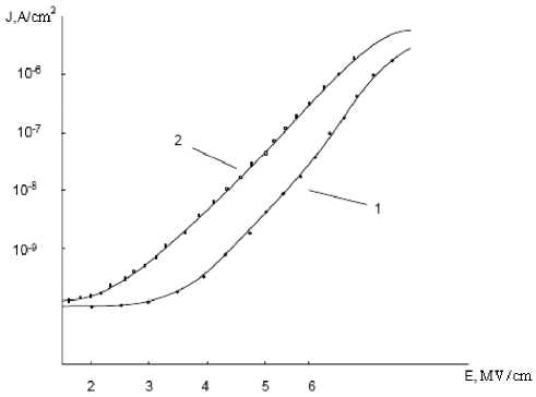
Fig. 1. VAC of OPs with various density of mobile charge N mc in a dielectric: 1 – N mc = 1∙1011 cm–2; 2 – N mc=1∙1012 cm–2
Changing of the form and position of VAC of the oxide on the surface of polysilicon is caused by the appearance of an additional internal electric field + directed along an external field and promoting the growth of currents of conductivity and reduction of dielectric strength of OPs [3] in a dielectric.
It is caused by a positive charge of ions (fig. 3).
According to the received data, this component arises under weak electric loadings < 2 MV/cm (fig. 1).
Now we should estimate the density of mobile charge
Nmc responsible for occurrence + bythedataofVAC (fig. 1). Like the calculation of density of mobile ions on the basis of VAC movement the definition of Nmc should be performed on the basis of the shift of VAC (AVmc) with respect to the theoretical curve corresponding to Nmc =0, for the chosen level of an electrical current density:
— Q C A V NE mc spec mc 0
N mc
.
qqq
Then we should calculate the density of mobile ions in
OPs (1) for the film Ps with the thickness of 50 nm and the degree of heterogeneity of the border Z = 1.1. In this case the shift AE = E+ on the level 10-10 А/ cm2 is approximately
Mathematics, mechanics, computer science
-
1 MV/cm. The density N mc corresponding to this shift is equal to:
N mc = ε⋅ε 0 ⋅ E +=
q
-
= 3.8 ⋅ 8.85 ⋅ 10 - 14 ⋅ 106 ≈ 2 ⋅ 1012m-2. (2)
-
1.6 ⋅ 10 - 19
At the same time the density of ions in this film, measured bythemethodofTSPcurrentis4∙1012 cm–2.
E dis
V/cm
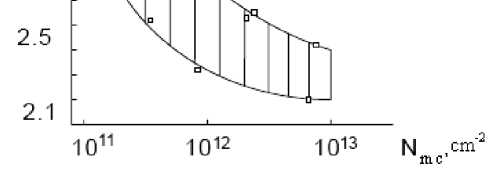
Fig. 2. The dielectric strength dis vs. average density of mobile charge N mc in OPs
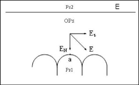
Fig. 3. Distribution of electric field in OPs near the edges of Ps
Hence, only half of ions in layer OPs makes the contribution to the change of internal electric field on a blocking surface. This result is in accordance with calculation data of the centroid of mobile charge in the oxide on the surface of polysilicon, which shows this charge located in the center. Thus, it confirms the conclusion about approximately equal distribution of ions on the internal and external interfaces. It means that the increasing of currents of conductivity in a low-voltage part of VAC of OPs is caused by the ionic charge placed near the oxidized surface of Ps.
At measurement of VAC the appearance of additional electronic currents caused by a positive ions field takes place at a room temperature under the redistribution of ionic charge along the heterogeneous blocking border. Redistribution of ions at measurement of VAC occurs permanently in accordance with a map of internal electric fields in time τrel.
Effectivetimeofrelaxationforsiliconoxide τ rel=10–5...10–3sec [4], thereforeinarangeofweakelectricfields p2MV/cmthetime of relaxation of a mobile ionic charge is:
ε
τ =τ ⋅exp a =(10-5...10-3)× rel eff .0
K ⋅ T
-
1.34 - 4.82 ⋅ 10 - 4 2 ⋅ 10 6
× exp = 1...600sec. (3) 0.025
Time of VAC registration τ reg fortheoxideof50nm thickness at the speed of scanning V reg =0,25V/sinthe specified limits of electric fields 2 MV/cm is:
τ =χ SiO2 ⋅ E = 2 ⋅ 10 - 6 ⋅ 2 ⋅ 10 6 = 4s. (4) reg v reg n 0.25
The comparison of τ rel and τ reg, estimations N mc using VAC and curves of TSP currents shows that only a part of charge of ions for which τ rel< τ reg, is shown as a change of conductivity of OPs.
The change of the relief of the geometrical border leads to redistribution of the internal electric field of mobile charge of ions. It is possible to predict, that at increasing the degree of heterogeneity of interface OPs – Ps there appears accumulation of ions on the edges of Ps and increasing of the local electric field. It is accompanied by displacement of VAC in the area of weak electric fields and reduction of steepness of VAC.
The presence of mobile positive charge in OPs and accumulation of this charge near the edges of polysilicon leads to the increasing of the local electric fields at the blocking border of Ps and growth of conductivity of an isolating layer. The electric field caused by ionic charge, accumulated on the edges of polysilicon, stimulates the injection of electrons from polysilicon. The influence of charge of mobile ions on conductivity of the oxide with heterogeneous geometrical interface become stronger or weaker at increasing or decreasing the degree of roughness of a blocking surface.
Bibliograghy
-
1. Han Sheng Lee. High electric field generated electron traps in oxide grown from polycrystalline silicon / Han Sheng Lee//Appl. Phys. Lett. 1980. Vol. 37. 12. P. 1080–1082.
-
2. Groesneken, G. A quantation model for the conduction in oxides thermally grown polycrystalline silicon / G. Groesneken, H. E. Maes // IEEE Trans. on El. Dev. 1986. Vol. ED-33. .7. P.1028–1042.
-
3., . .
/
-
4. Salman, E. G. Thermally stimulated depolarization current controlled by surface charge change / E. G. Salman, V. N. Vertoprakhov // Phys. Stat. Sol. (a). 1988. Vol. 1008. 2. P.625–630.
.. ,.. ,...
. . : 558-76.,
