The method of synthesis of the digital controller for a solar energy conversion channel of the solar battery in the power supply system of a spacecraft

Author: Shkolnyi V.N., Semenov V.D., Kabirov V.A., Sukhorukov M.P., Torgaeva D.S.
Journal: Сибирский аэрокосмический журнал @vestnik-sibsau
Section: Авиационная и ракетно-космическая техника
Article in issue: 1 т.20, 2019.
Free access
A method of synthesizing a digital controller for a solar energy conversion channel in a power supply system of a spacecraft is presented. The method is based on the initial functional diagram of the pulse converter and the method of switching discontinuous functions. In accordance with the technique, which is formally presented in the form of eight consecutively executed items, a block diagram of the shunt converter has been developed in the basis of switching func- tions, which is taken as an example for testing the technique. The shunt converter is one of the three energy conversion channels in modern power supply systems of a spacecraft. The block diagram showed that all nonlinearity of the system can be reduced to nonlinearities of two multiplication links and nonlinearity of a pulse-width modulator. The possibility and acceptability of joint linearization of each of the specified nonlinear multipliers with a pulse-width modulator at the selected operating point is shown. A linearized block diagram of the control object was obtained, after which the trans- formation and simplification of the block diagram to a convenient form for calculation was carried out. Using the trans- fer functions of the linearized block diagram, the logarithmic frequency characteristics were calculated analytically and the results of their comparison with the frequency characteristics obtained experimentally on a simulation model, which confirmed their identity in the working frequency domain, were presented. At the same time, the specified simulation model of a shunt pulse converter, built in the Simulink package of the Matlab design environment, took into account all the mentioned nonlinearities of the real converter. According to the obtained logarithmic characteristics, a classical synthesis of the analogue prototype correcting section was produced. The transition from the analog correcting section of the prototype to the implementation of the digital correcting section is shown. Simulation modeling of a closed-loop power supply system with a synthesized analog controller, in its mode of operation from a solar battery, confirmed the correctness of the methodology and the achievement of the goals. The results of the work are intended to create a new onboard energy conversion equipment for power supply systems of high-potential spacecrafts. The scope of application of the project results is space instrumentation.
Synthesis of digital controller, technical optimum, simulation modeling, shunt converter, power supply system, spacecraft
Short address: https://sciup.org/148321899
IDR: 148321899 | UDC: 621.316.71 | DOI: 10.31772/2587-6066-2019-20-1-74-86
Методика синтеза цифрового регулятора для канала преобразования энергии солнечной батареи в системе электропитания космического аппарата
Представлена методика синтеза цифрового регулятора для канала преобразования энергии солнечной ба- тареи в системе электропитания космического аппарата, основанная на исходной функциональной схеме им- пульсного преобразователя и методе коммутационных разрывных функций. В соответствии с методикой, формально представленной в виде восьми последовательно выполняемых пунктов, в базисе коммутационных функций разработана структурная схема шунтового преобразователя, который взят в качестве примера для проверки методики. Шунтовой преобразователь является одним из трех каналов преобразования энергии в современных системах электропитания космических аппаратов. Структурная схема показала, что все нелинейности системы можно свести к нелинейностям двух звеньев умножения и нелинейности широтно- импульсного модулятора. Показана возможность и допустимость совместной линеаризации каждого из указанных нелинейных звеньев умножителей с широтно-импульсным модулятором в выбранной рабочей точке. Получена линеаризованная структурная схема объекта управления, после чего проведено преобразо- вание и упрощение структурной схемы к удобному для расчета виду. По передаточным функциям линеари- зованной структурной схемы аналитически рассчитаны логарифмические частотные характеристики и приведены результаты их сравнения с частотными характеристиками, снятыми экспериментально на имитационной модели, которые подтвердили их идентичность в рабочей частотной области. При этом указанная имитационная модель шунтового импульсного преобразователя, построенная в пакете Simulink среды проектирования Matlab, учитывала все упомянутые нелинейности реального преобразовате- ля. По полученным логарифмическим характеристикам произведен классический синтез аналогового корректирующего звена прототипа. Показан переход от аналогового корректирующего звена прототипа к реализации цифрового корректирующего звена. Имитационное моделирование замкнутой системы элек- тропитания с синтезированным аналоговым регулятором в режиме ее работы от солнечной батареи подтвердило правильность методики и достижение поставленных целей. Результаты работы предназна- чены для создания новой бортовой энергопреобразующей аппаратуры систем электропитания перспек- тивных космических аппаратов. Областью применения результатов проекта является космическое при- боростроение.
Text of the scientific article The method of synthesis of the digital controller for a solar energy conversion channel of the solar battery in the power supply system of a spacecraft
Introduction. One of the most important onboard systems of automatic spacecraft (SC) is the power supply system (PSS), which is a combination of primary and secondary current sources, energy conversion equipment and output voltage stabilization with the necessary control and automation [1; 2].
When developing a PSS of a SC, it is necessary to take into account many disturbing influences that affect the quality of the output voltage, the static and dynamic characteristics of the PSS adversely. Such impacts include changes in load resistance and power supply sources, degradation of primary energy sources, etc., which, in turn, leads to the need in building an automatic control system that ensures stable PSS operation with a given accuracy over the entire range of changes in these disturbances.
At present, control systems (CS) on an analog element base [3–7], which are often called analog control systems for short, are widely used in the PSS of a SC. When solving problems of improving the reliability of the PSS and at the same time improving its overall mass and functional characteristics, it becomes obvious that analog control systems fit the physical limit of the possibility of improving their functional parameters and overall mass characteristics [8].
The next stage in the development of the PSS of a SC is the transition to control systems built on a digital element base, also called digital control systems (DCS). Digital control systems, compared to analogue CSs, can provide [9] higher reliability, reduced weight and dimensions of the power supply system (including the cable космический аппарат.
network), and electronic anticountermeasures of transmission of the control signal.
In addition, digital control will allow to expand the functionality of the CS, simplify the creation of their modifications and embeddability of various devices in the structure. Digital control systems for their intended purpose allow to exchange data with the on-board control complex over a high-speed data interface, and this function is already widely used. However, the systems of direct digital control of energy-converting equipment, including pulse converters of electrical energy parameters, despite these obvious advantages, are practically not used at the moment, and analog control systems are widely used. This situation in the field of direct digital control systems application is connected with the fact that digital systems contain analog-digital converters, digital blocks for implementing signal modulators and digital communication interfaces for closing negative feedback circuits. Аs it is well known digital nodes and blocks cause delays in signals that are similar in nature to breaks of transport delays, which complicates the synthesis of correcting sections greatly.
Purpose. The purpose of this work is to develop a method of synthesis of the digital controller for a solar energy conversion channel of a solar battery in a power supply system of a spacecraft.
Method of synthesis of the digital controller.
The method of synthesis of the digital controller will be considered in the following sequence:
-
1. Develop a mathematical model of a pulse converter (control object) in the form of a block diagram con-
- structed in the basis of discontinuous switching functions according to a given functional diagram.
-
2. Select nonlinear links and linearize them at a given operating point on the block diagram obtained in the basis of discontinuous switching functions, presenting each nonlinear link by a combination of linearized links, in order to obtain a linearized block diagram of the control object.
-
3. Determine the necessary transfer functions of the system, including the linearized transfer function of the open-ended control object based on the obtained linearized block diagram.
-
4. Compare the frequency characteristics of the linearized open unadjusted control object, obtained from its linearized transmission links, with the experimental “low-signal” frequency characteristics of the open unadjusted control object, taken on its simulation model built in the Simulink package of the Matlab design environment; if the compared frequency characteristics coincide with a given quantitative accuracy, the linearized model can be considered adequate.
-
5. Build a family of frequency characteristics of an open unadjusted control object using its linearized transfer functions at the “extreme” operating points of the system, meaning the “extreme” working points of the steady state point of the controlled object at the minimum and maximum values of all disturbing factors.
-
6. Synthesize the necessary type of analog correction link and its parameters assuming that the linearized model adequately describes the open control object and using the classical methods of synthesizing linear control systems for this reason.
-
7. Build a simulation model (for example, in the Simulink package of the Matlab design environment) of a closed-loop control system with the parameters of the corrective element obtained in step 6, and check the static and dynamic characteristics of the synthesized analogue controller.
-
8. Make a z-transformation of the transfer function of the discrete circuit and synthesize a digital correction link using the known transfer function of the analog correction link and a bilinear transition. If necessary, check the dy-
- namic characteristics of the automatic control system (ACS) with a digital correction link on the simulation model in the Matlab environment, taking into account the delay.
The control object for the direct digital control system is the voltage stabilization module (VSM) of the energyconversion complex, which includes three types of energy conversion channels:
– “SlB conversion channel” intended to convert the energy of on-board solar batteries into a constant stabilized output bus voltage to which the load is connected;
– “memory conversion channel” intended for charging onboard batteries with a stabilized current, the value of which can be changed by an external signal;
– “StB conversion channel” intended to convert the energy of the on-board storage batteries into a constant stabilized voltage of the output bus to which the load is connected;
Each of the energy conversion channels is a power pulse converter of electrical energy with or without feedback, providing a given law of operation. It can be made on the basis of parallel connection of several pulse converters. The number of channels, the number of parallel-connected converters in the channel and the order of their inclusion is determined by the load power, the number of solar and rechargeable batteries, and the accepted operation algorithm.
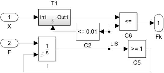
Let us consider the PSS of a SC when operating a SlB conversion channel, made on the basis of a shunt converter (fig. 1), on the topology of a boost converter ( L 1, VT 1, VD 1, C 3) with negative feedback implemented by a digital control system (DCS). Since the solar battery operates on the current branch of its current-voltage characteristic, it was represented in this diagram as a current source I SlB . The feedback signal U f from the voltage sensor VS, connected to the output of the SlB channel, is converted by the ADC into digital for, subtracted from the signal of the setting voltage u and then through the correcting element CS, the digital pulse-width modulator PWM and driver D are fed to the power switch VT 1 of the shunt converter.
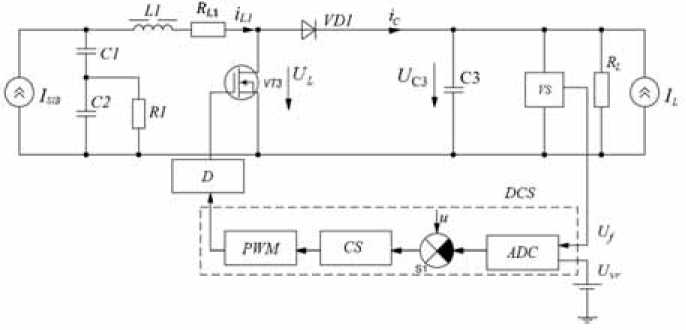
Fig. 1. Functional diagram of the shunt converter with a digital control system
Рис. 1. Функциональная схема шунтового преобразователя с цифровой системой управления
The scheme uses a pulse-width modulator of the first kind (PWM1) with a delay of one sweep signal. It is PWM1 that is implemented in digital control systems based on microcontrollers. The current source I L is designed to simulate the disturbing effect of the load current on the stabilization system. The input filter, assembled on elements С 1, С 2, R 1, is intended [10] for smoothing the voltage ripples on the solar battery (current source I SlB). The output filter С 3 is designed to smooth the ripple on the load, indicated by the equivalent resistance R L .
To implement the proposed method for the synthesis of a corrective element, in accordance with step 1, it is necessary to present a mathematical model of a shunt energy converter in the form of a structural diagram built in the basis of discontinuous switching functions. The digital control system, at this stage of the study, is considered ideal, assuming that the ADC performs the conversion instantaneously with infinitely high frequency, and the adder S1 and the corrective section of the short circuit are equivalent under these assumptions to the ideal analog link. Such a structural scheme, built according to the method described in [11], is presented in fig. 2. This block diagram is obtained by representing the inductances L and the capacities C of the shunt converter by ideal integrators with the corresponding coefficients 1/ L and 1/ C . The resistors in the power circuit of the shunt converter are replaced by instantaneous links with transfer coefficients R , if it is a current-to-voltage link, or 1/ R , if it is a voltage-to-current link. The summation of voltages and currents in the respective voltage circuits and current nodes reflect the adders S1 – S6 of the block diagram. The key part of the shunt converter, consisting of the power transistor VT1 and diode VD1 , is represented by two unidirectional controlled transmission links made in the form of multipliers marked with X . And one of the links X 1 plays the role of the current transfer link i L 1 of the input choke L 1 to the output capacitor C 3, and the second X 2 takes the role of the transmission link of the output voltage U C 3 in the input circuit of the choke L 1. Both links of the multipliers X 1 and X 2 are controlled by a common signal (1– FK ( t )), which is fed to their control inputs. As it was mentioned above, an ideal digital control system is analog and consists of an instantaneous voltage sensor with a transfer coefficient Cs ; source of voltage u ( t ); adder S 7; analog model of the correcting section (AMCS), with an unknown transfer function and analog model of a pulse-width modulator (AM PWM), which in its turn converts a continuous signal x ( t ) acting on the output of the AMCS in a pulse signal F K ( t ), which is a switching function of the shunt converter, and accepts values “0” or “1”. The analog models of the corrective link of the AMCS and the pulse-width modulator AM PWM will be understood as some decisive blocks of an analog computer that implement the corresponding signal conversion functions. This condition will allow us to present block diagrams in the form of temporary functions.
The block diagram of fig. 2 which is built in the basis of switching discontinuous functions, clearly shows all the internal feedbacks of the shunt converter and the role that these connections play in the system, and also allows one to select non-linear transmission links.
In this diagram, the nonlinear signal transmission links are the pulse-width modulator PWM (its analog model) and the multipliers X 1, X 2, which are described by the relations
iC (t ) = [1 - FK(t )]• iL 1(t), uL (t) = [1 - FK(t )]• uC3(t),
where iC ( t ), uL ( t ) – are output signals of multipliers X 1, X 2; iL 1( t ), uC 3( t ) – are input signals of the multipliers (state variables of the described dynamic system), which are fed to the "power" input of the corresponding multiplier; [1– F K ( t )] is a control signal that is generated by a PWM block and is fed to the control inputs of both multipliers.
Assuming that the continuous part of the SlB transform channel (control object) has the properties of a low-pass filter, which is naturally always performed with high quality requirements for the output voltage, the impulse switching function [1– F K( t )] can be reduced to a continuous function. Indeed, in the steady state operation of the system, a continuous signal x ( t ) at the input of AM PWM can be represented as the sum of the constant component of the signal Х 0 , which characterizes the operating point of the steady state mode, and the small deviation d x of this signal from X 0 . In this case, the output of AM PWM sets the switching function F K0 , the relative duration of which will correspond to the signal X 0 , if the signal x ( t ) is normalized and its maximum value is equal to one. Thus, under the condition of signal normalization x ( t ), expressions (1), describing the operation of multipliers, can be rewritten in the form (2), where the time dependence of the values used is not indicated to simplify the expression.
i C =( 1 - x ) • i L 1 , u L = ( 1 - x )• iC 3 .
Since now expressions (2) describe the product of continuous functions, they can be linearized by the formula for finding the differential of the product, which allows us to obtain diC (1 X0 )• diL 1 IL 10 • dx, duL = (1 — Xо) • dueз — Uc30 • dx,
where di C , di L 1 , du L , du C 3 , dx – are small deviations of the corresponding signals from their steady-state values I C 0 , I L 0 , U L 0 , U C 30 , X 0 . According to expressions (3), each of the multipliers and analog models of PWM, which are nonlinear links, are replaced by two linear instantaneous links [12] with transfer coefficients (1– X 0), IL 10 and (1– X 0), UC 30, respectively, as well as adders (subtractors ) S 8 and S 9, as shown in fig. 3. Since the rest sections of the block diagram in fig. 2 are linear, then the whole system becomes linearized. However, it should be remembered that in a linearized system, the variables are small deviations of signals from their steady-state value, therefore these signals are marked with a “tilde” icon.
Further simplification of the linearized block diagram and its reduction to the form shown in fig. 4 is a cumbersome task rather than a complex one.
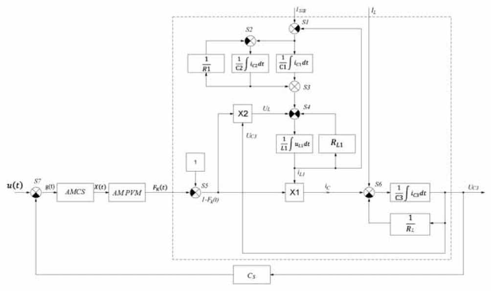
Fig. 2. Block diagram of the shunt converter with input filter and control system
Рис. 2. Структурная схема шунтового преобразователя с входным фильтром и системой управления
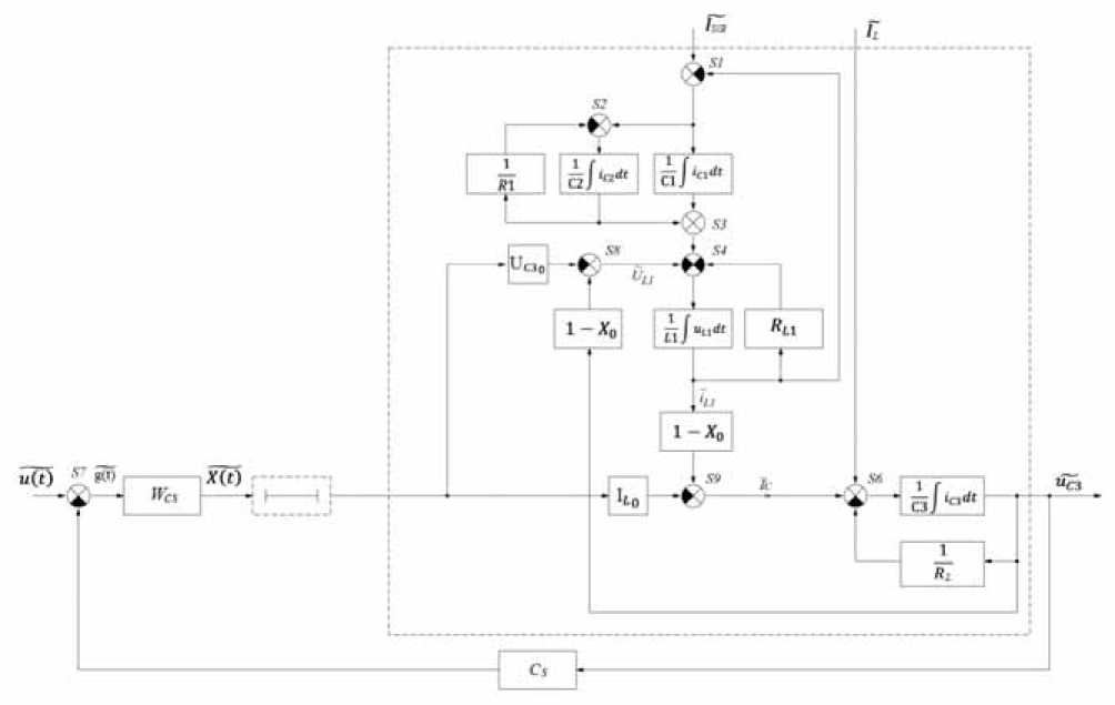
Fig. 3. Linearized block diagram of the shunt converter with input filter and control system
Рис. 3. Линеаризованная структурная схема шунтового преобразователя с входным фильтром и системой управления
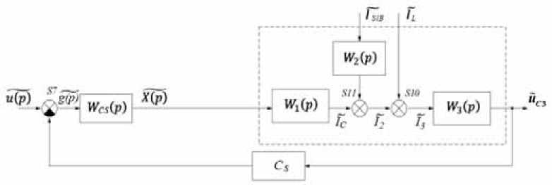
Fig. 4. Simplified linearized mathematical model of the shunt converter with input filter and control system
Рис. 4. Упрощенная линеаризованная математическая модель шунтового преобразователя с входным фильтром и системой управления
Formulas 4–6 allow us to determine the transfer functions of the links W 1 ( p ) – W 3 ( p ) shown in fig. 4
W(pA = IC ( P ) = p ) X ( p )
U • — •
C 30
0 RL 1
R L 1
•
L 1
---P + 1
R L 1
L 1
--- P + 1
R L 1
( 1
R 1
I L o
;
C 1 p R1C 2 p + 1
W2 ( p ) =
R L 1
•
L 1
— p + 1
R L 1
I 2 ( P ) = I SlB ( P )
R 1
C 1 P R1C 2 P + 1
•
R „ ( L1 1
L 1 p + 1
I R l 1 .
R 1
1 + 1
C 1 p R1C 2 p + 1
W ( P ) =U f 2^^ ) =
I 3 ( P )
R , Г 1 1 ( 1 R 1 ) ,
• -1+ 1
R L C 3 P + 1 R L 1 ( L 1 p + 1 A ( C 1 P R 1 C 2 P + 1 J
R L
R L C 3 p + 1
•
1 R L 1
•

• ( 1 - X 0 )2
+ R L 1
•
L 1
— P + 1
R L 1
R 1
--------7 1 + 1
C 1 P R1C 2 P + 1
Checking the adequacy of the obtained linearized structural diagram in fig. 3 and the simplified block diagram in fig. 4, which can also be called small-signal models of the system, is carried out according to the method
given in [13]. This technique means to make a simulation model of a pulsed shunt converter with open-loop feedback in the software design environment Matlab.
Simulink; to take down logarithmic amplitude and phase-frequency characteristics on this model using the means provided by the software environment during the experiment; to compare the characteristics obtained experimentally on the model, with the characteristics calculated by the small-signal model (linearized block diagram) with a broken feedback loop. Feedback loop in fig. 3 is broken at the output of the analog model of the correcting section AMCS, and the delay link, shown conventionally by a dotted line, is not yet taken into account. This means that in the synthesis of the transfer function of the correcting element, the influence of the delay is neglected. The test signal is sent to the system input x ( t ) = X 0 + ( dx )^sin ®t , while X 0 determines the operating point of the steady state, the “small” amplitude dx of the sine determines the small deviation from the operating point, and the frequency to changes in the desired range. The transfer function of an open object with respect to a control action, the adequacy of which is further proved, will have the form (7), with Ĩ L = 0 и Ĩ SlB = 0.
Wy ( P ) =
*w
UС 3 ( p ) X ( p )
= W(P ) • W 2 ( P ).
The results of such a test are presented in fig. 5. Dependencies shown in fig. 5 confirm the adequacy of the linearized block diagram in fig. 3 and the simplified scheme in fig. 4 in the considered frequency range.
To determine the parameters of the correcting section, in accordance with paragraph 6 of the proposed methodology, it is necessary to build a family of Bode diagrams of an open loop uncorrected system at the “extreme” operating points. The definition of “extreme” operating points becomes clear if we pay attention to the fact that in expressions 4–6, the electrical parameters of the circuit characterizing its mode of operation are used as transfer coefficients of the links, for example, U C30 , X 0 , I L0 , which, in turn, depend on current I SlB and load resistance R L . Fig. 6, a shows the families of characteristics when the current of the solar battery I SlB is changed and the load
resistance R L is in the range from their minimum value to the maximum, which explains the use of the term “extreme” operating points.
Based on this family of characteristics, obtained according to a linearized block diagram and presented in fig. 6, a , in accordance with paragraph 6 of the proposed methodology, the type of correcting section (7) and its coefficients were synthesized:
W CS ( p )=
^
X(p) = K^. Tp + 1 , g ( P ) kr P ( T2 P + 1)
where K = 2,4∙104 с–1; T = 0,005 с; T = 6,6∙10–6. kr 1 2
The Bode diagrams of the corrected system, corresponding to the same “extreme” points of the variation range of the parameters, are presented in fig. 6, b , from which it is possible to determine the obtained stability reserves (16 dB, 35 degrees) with the worst combinations of the considered parameters.
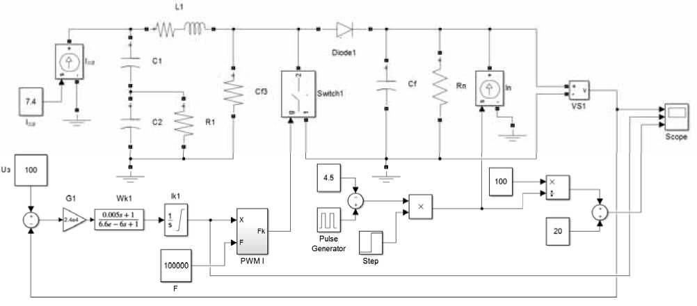
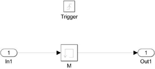
To test the dynamic characteristics of the SlB channel, in the Simulink package of the Matlab design environment, its simulation model was built (fig. 7, a) with closed feedback and a synthesized analog correcting section (8). The model parameters are presented in table, the internal structure of the PWM1 unit is shown in fig. 7, b, and the scheme of the T1 trigger subsystem is shown in fig. 7, c. If it is necessary, the proposed simulation model can take into account and verify the effect of the delay section, which, according to the authors of [14], does not allow accurate calculation of the correcting section parameters and requires their experimental verification.
The results of the simulation modeling of the SC PSS during SlB channel operation with closed feedback and a synthesized corrective link are shown in fig. 8.
Analysis of the simulation modeling results shows that when the In load current varies in the range from 3 to 7 A, the steady-state voltage Un on the power bus of the power supply load does not change, which indicates a zero static control error. From the given time diagrams it can be seen that with sharp changes in the load current I n , the voltage spikes U n do not go beyond the permissible range. The overshoot of voltage during load dropping is 0.8 %, the voltage fall during load rise is 0.94 %, the durations of transient processes during loading current dropping and rise are 3.3 ms and 4.3 ms respectively.
The obtained transfer functions and the achieved dynamic characteristics correspond to the analog correcting section. To determine the parameters of the transfer function of the corresponding discrete correcting section, it is necessary to implement the bilinear form of the transition from the Laplace transform to the z -transform, by replacing the Laplace operator p [15] in the transfer function Wcs ( p ) (analogue function of the prototype):
W cs ( z ) = W cs ( P )| p , When P = 2 ( 2 , (9) p T I z + 1 )
where T is the sampling period of the digital correcting section. After that, it is necessary to reduce the transfer function to the canonical form (10).
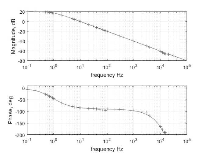
Fig. 5 Bode diagrams in the nominal mode of operation constructed on the small-signal model of the expression (7) (solid lines) and taken on the simulation model (marked with a “+ ” sign)
Рис. 5. ЛАЧХ и ЛФЧХ в номинальном режиме работы, построенные по малосигнальной модели выражение (7) (сплошные линии) и снятые на имитационной модели (помечены знаком «+»)
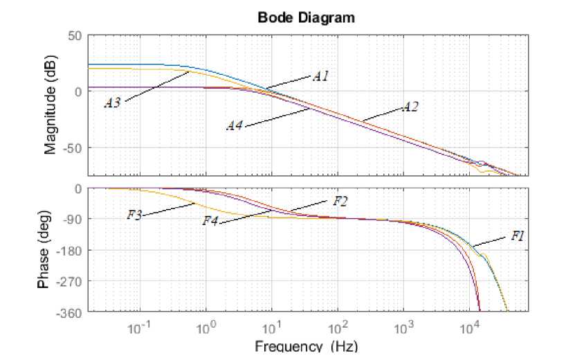
а
A1, F1: Х 0 = 0.9324, I SlB = 7.4А, R L = 200Ω
A2, F2: Х 0 = 0.3243, I SlB = 7.4А, R L = 20Ω
A3, F3: Х 0 = 0.8936, I SlB = 4.7А, R L = 200Ω
A4, F4: Х 0 = 0.2908, I SlB = 4.7А, R L = 30Ω
b
Fig. 6. Bode diagrams: а – open-loop uncorrected system; b – open-loop corrected system
Рис. 6. Логарифмические частотные характеристики: а – разомкнутой нескорректированной системы; b – разомкнутой скорректированной системы
c
Fig. 7. Simulation model:
а – energy conversion channel SlB; b – subsystem model PWM1; c – subsystem model Т 1
Рис. 7. Имитационная модель:
а – канала преобразования энергии БС; b – модель подсистемы ШИМ I; c – модель подсистемы Т 1
The parameters of the simulation model elements of the shunt converter
|
Symbol |
Value |
Symbol |
Value |
|
С 1 |
1 µF |
R L |
Varies in range 13.5 ... 135 Ohm |
|
С 2 |
1 µF |
I SlB |
7.4 А |
|
R 1 |
10 Ohm |
I L |
Impulse: from 0 to 4 А. |
|
L 1 |
170 µF |
Diode1, Switch 1 |
Ideal |
|
R L1 |
33 mOhm |
F |
100000Hrz |
|
C 3 |
1200 µF |
Uз |
Setpoint voltage: 1V |
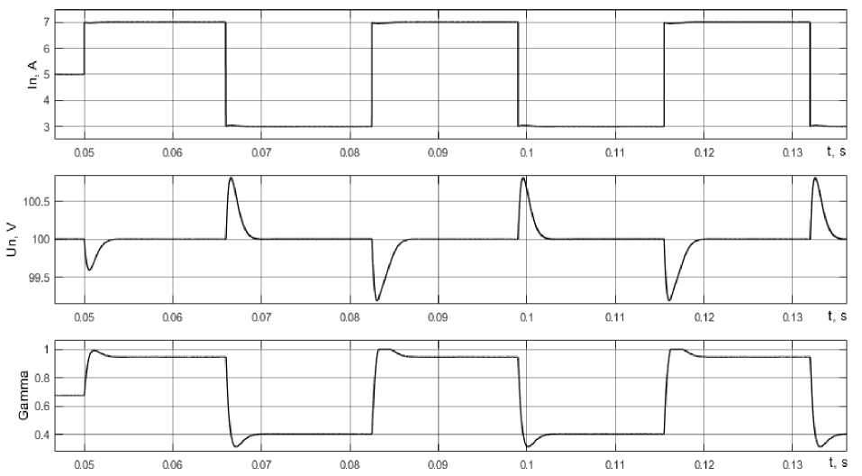
Fig. 8. Timing diagrams of the load current ( I n ), on-load voltage ( U n ), the control signal at the input of the PWM modulator of the SlB channel (Gamma)
Рис. 8. Временные диаграммы тока нагрузки ( In ), напряжения на нагрузке ( Un ), сигнала управления на входе ШИМ-модулятора канала БС (Gamma)
For the transfer function of the correcting section with the parameters specified in (8), the coefficients of expression (10) have the following numerical values: b 0 = 51.7759; b 1 = 0.1034; b 2 = –51.6724; a 1 = 1.1380; a 2 = –0.1380; T = 10–5 с.
W cs (z) =
( b o + b 1 z - 1 + b 2 z - 2 ) ( 1 - a 1 z - 1 - a 2 z - 2 )
Expression (10) makes it easy to go to the recurrence relation (11) and the difference equation (12)
mn
x [ i ] = Z bj' g [ i — j ] ' Z аГ xi — j ], (11)
j = 0 j = 1
where j = 0,1... m - is the number of coefficients in the expression (10), i – is the current reading of the input g ( i ) and output x ( i ) signals of the correcting section
x(k) = b ■ g(k) + b1 ■ g(k — 1) + b2 ■ g(k — 2) - a1 x x x(k -1) - a2 ■ x(k - 2). (12)
Differential equation (12) allows us to calculate the output signal of the digital correcting section from the readings of the input signal, thus realizing the digital implementation of the obtained analog correcting section, in accordance with paragraph 9 of the proposed method. The loading diagram of the synthesized correcting section, which is also a numerical simulation model of a digital controller, is shown in fig. 9. This scheme is constructed according to expression (12), and the z –1 link presented in the diagram is a delay link for one sampling rate period.
Fig. 10 shows the timing diagrams of the output voltage, obtained by abruptly changing the load current, with analog and digital correcting sections.
The diagrams shown in fig. 10 are obtained on a simulation model of a closed SAR (fig. 7) with an analog correcting section, the parameters of which are given on the model, and with a digital correcting section (10) under the same conditions as the SAR with an analog correcting section.
Comparison of timing diagrams in fig. 10 with timing diagrams in fig. 8 shows that they differ quantitatively by no more than 0.01–0.02 V, that is, they practically coincide.
Conclusion. The method of synthesizing a digital controller for a channel of converting the solar battery energy in a power supply system of a spacecraft based on a block diagram of a converter and on the method of switching discontinuous functions has been developed.
On the basis of the proposed methodology, the type and coefficients of the correcting section were selected, providing the necessary stability stocks.
The parameters of the correcting section are chosen so that the characteristics of the system are close to the settings of the technical optimum.
It was shown on the simulation model built in the Simulink package of the Matlab design environment that with the selected type of correcting section and the selected numerical values of its coefficients, the system ensures stable operation throughout the claimed range of disturbance changes. This suggests that, despite the presence of delays in the digital information processing channel and in the PWM channel, the proposed method allows us to synthesize a digital control system of a power supply device for a spacecraft that meets the specified requirements for accuracy and speed.
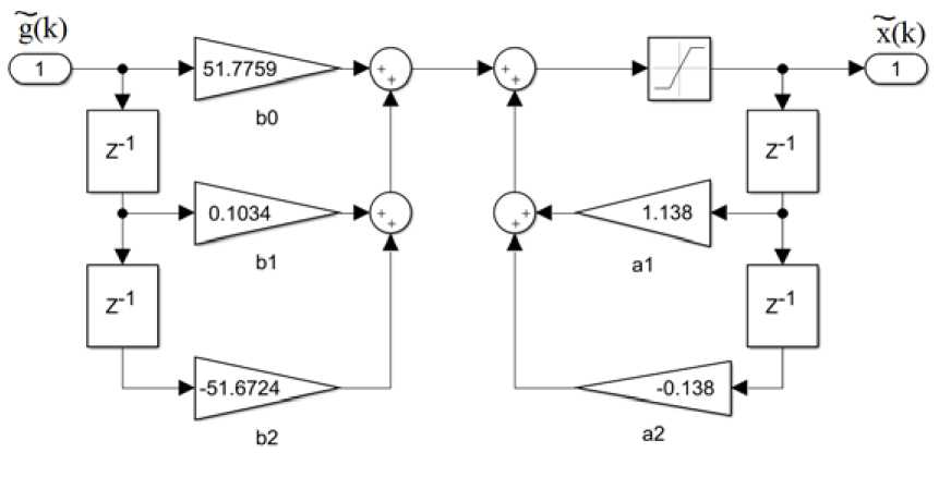
Fig. 9. Simulation model of the digital controller
Рис. 9. Имитационная модель цифрового регулятора
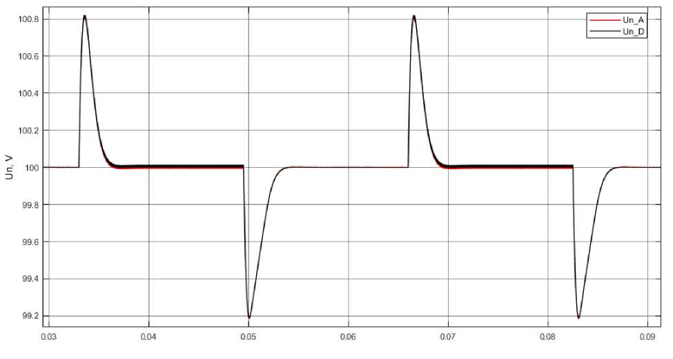
Fig. 10. Timing diagrams of the output voltage with an abrupt change in the load current, obtained in a system with analog and digital correcting sections
Рис. 10. Временные диаграммы выходного напряжения при скачкообразном изменении тока нагрузки, полученные в системе с аналоговым и цифровым корректирующими звеньями
Acknowledgements. The work was performed in the framework of implementation of the RF Government Decree from April 9, 2010 No. 218, and the contract between the JSC “ISS” and the Ministry of Education and Science of the Russian Federation from December 1, 2015 № 02.G25.31.018.
References The method of synthesis of the digital controller for a solar energy conversion channel of the solar battery in the power supply system of a spacecraft
- Шиняков Ю. А. Энергетический анализ структурных схем систем электроснабжения автоматических космических аппаратов//Известия Томского политехнического университета. 2006. Т. 309, № 8. С. 152-155.
- Системы электропитания космических аппаратов/Б. П. Соустин, В. И. Иванчура, А. И. Чернышев, Ш. Н. Исляев. Новосибирск: ВО «Наука»; Сибирская издательская фирма, 1994. 318 с.
- Super power subsystem development and application on the 1300 family of spacecraft/C. Greenwood, S. Lenhart, B. Inenaga //20th AIAA International Communication Satellite Systems Conference and Exhibit 12-15, May 2002.
- Abbas A. In-Orbit Performance of Lockheed Martin's Electrical Power Subsystem for A2100 Communication Satellite//AIAA. 2000. 28 p.
- A power conditioning unit for high power geo satellites based on the sequential switching shunt series regulator/A. Garrigos, J. A. Carrasco, J. M. Blanes, E. Sanchis-Kilders//IEEE MELECON Electrotechnical Conference. May 16-19, 2006. P. 1186-1189.
