VLSI implementation of CMOS full adders with low leakage power

Author: Manisha B. S., Rudraswamy S. B.
Journal: International Journal of Computer Network and Information Security @ijcnis
Article in issue: 4 vol.10, 2018.
Free access
In this paper, we present two different methods to implement 1-bit full adder namely MTJ based full adder design also called MFA and Lector method based full adder design. These adders are designed and implemented using CADENCE Design Suite 6.1.6 Virtuoso ADE. The implemented design is verified using CADENCE ASSURA. The performance is measured for 45nm technology and a comparative analysis of transistor count; delay and power of the adders were performed. When compared with the previous MFA the proposed MFA overcomes the SEU error which is a result of body biasing. In Lector technique the transistor density is reduced by implementing the sum logic in terms of carry thus reducing the area. In order to attain the complete logic levels buffers are introduced at the sum and carry outputs of both Lector and MFA. The Lector method uses less number of transistors when compared with proposed MFA, but the proposed MFA is efficient because it achieves minimum power dissipation when compared to the Lector method.
Magnetic Full Adder (MFA), Magnetic Tunnel Junction (MTJ), Single Event Upset (SEU), Spin Transfer Torque (STT)
Short address: https://sciup.org/15015591
IDR: 15015591 | DOI: 10.5815/ijcnis.2018.04.03
Text of the scientific article VLSI implementation of CMOS full adders with low leakage power
During the past decades, speed or performance was the major issues in CMOS VLSI design. At present power dissipation has become the major issue when the systems are built using millions and millions of transistors, leakage current has become a dominant factor when compared to switching current when technology shrinks further and further. The challenge faced by the evolution of integrated circuits is the utilization of large power. The incorporation of higher clock rates, miniature process geometries and greater functional integration has given rise to increasing power density. Due to the scaling speed of operation increases which results in higher performance of a transistor also scaling enhances transistor density and functionality. To gain the performance threshold voltages must also decrease along with geometries, but leakage current increases with the reduction in threshold voltage. Due to scaling of geometries thinner gate oxides is obtained which has given rise to rapid growth in gate leakage current. At present leakage power has turned out to be a predominant problem. The sub-threshold leakage current is the main component of leakage, which increases exponentially with decreasing device dimensions. In 65 nm technologies and below, leakage current contributes for thirty to forty percent of power dissipation. Reduction of leakage power is of main interest for VLSI circuit designers, for recent CMOS feature sizes. Power consumption in CMOS circuits consists of two elements they are dynamic and static components. The dynamic power is caused by the switching activities in the circuits and also in CMOS devices current flow even when the transistors are off which causes leakage power loss and this power loss is called leakage or static power dissipation. At 0.18μm technology and above dynamic power consumption was of main interest for designing low-power chip as dynamic power consumption contributes to greater than 90% of the overall power of the chip. The main aim of voltage and frequency scaling was minimizing the dynamic power. But, the decrease in feature size has caused static or standby power dissipation to become a major problem for present and future technologies.
Over the past several years the driving force behind the great improvement in functionality, power and performance in integrated circuits is technology scaling. As a result of miniaturization and due to emerging trend in VLSI, power dissipation has turned out to be an extremely important design metric. For deep-submicron systems, threshold and supply voltages for transistors are minimized. To some extent, the reduction of voltages reduces the dynamic power dissipation, but there is a hike in sub-threshold leakage current which causes an increase in static power dissipation. The challenge faced by the reduction in feature size of CMOS devices is the rise in sub-threshold leakage current as a result of threshold reduction. Leakage current is of prime importance for high performance and digital CMOS circuits with low- power. Since supply voltages are scaled scaling of the threshold voltage is necessary in order to achieve excellent performance in active mode.
In Nanoscale technologies of CMOS devices leakage has become a main concern. Due to miniaturization in CMOS technology, leakage power is becoming equivalent to dynamic power. Due to extended battery life necessity of mobile devices and increasing transistor density in VLSI chips, power optimization is the main concern in today’s VLSI design. One-bit full adder in VLSI circuit is the basic gate utilized in adders/Subtractor, multipliers and Arithmetic and Logic Units etc and thus the overall system performance can be enhanced by improving the performance of a full adder [1-7].
II. Related Work
One of the major streams of VLSI Design is CMOS Technology. Dynamic or switching power is one of the major components of total power consumption in 0.18μ technology and above. But static or Leakage power dominates the dynamic power when technology feature size shrinks below 0.13μ technology. Several methods to reduce the leakage power have been proposed by the designers [12].
The methods proposed by V.Elamaran et al.[1] is a comparison study of a one-bit adder using different methods to reduce static power dissipation in digital circuits such as sleepy, stack, sleepy stack and sleepy keeper approaches but in all methods the area occupied, delay and also the static power consumption is more.
Pushpa Saini et al.[2] proposed new methods such as Sleep Transistor approach with NMOS, Sleep forced NMOS stack, Variable body biasing with bypass for the reduction of leakage power in 90nm technology. The designed methods were compared with the previous leakage reduction techniques. The sleep technique is combined with the other techniques as sleep is state destructive technique and hence these methods occupy more area.
An ultra low power non-volatile CMOS full adder by Ramin Rajaei et al.[5] is a low power Magnetic Full Adder (MFA) that can be used in advanced microprocessors, the MFA that is designed is capable of tolerating Single Event Upset (SEU) which is caused by particle strike without considering the induced charge when compared with the previous work. In the above proposed method the first MFA circuit changes the state when a particle strike and the circuit proposed to overcome this problem is complex circuits with increased number of transistors.
To reduce the leakage power Shashank Gautam [14] proposed techniques like MT CMOS, power gating, dual stack, galeor and lector. A Full Adder has been designed using these techniques and power dissipation is calculated and is compared with general CMOS logic of Full Adder. The lector and galeor techniques are efficient when compared to other techniques.
Amit Kumar et al.[17] proposed a power efficient Fulladder with body biasing. The Body-biasing technique is used to vary the threshold voltage to operate this adder at higher speed by allowing the faster gate switching. The proposed design is having delay and power merits.
Erya Deng et al.[8] proposed a magnetic full-adder (MFA) design that is novel and which is based on STT-MRAM with perpendicular magnetic anisotropy (PMA). When compared with traditional CMOS only full adder provides advantageous power efficiency and die area. This architecture allows scaling down the die area reducing energy consumption, as there is nearly zero standby power. But the MFA is more prone to radiation errors.
Robust Magnetic Full-Adder with Voltage Sensing 2T/2MTJ Cell proposed by Guillaume Prenat et al.[9] is a unique representation of Magnetic Full Adder (MFA) where all input signals are saved in non-volatile elements. Input data cin is stored in MFA through the MTJs that are fixed, while two voltage sensing 2T/2MTJ cells stores other two input data A and B. MFA is validated and its low consumption, great robustness and huge speed performance merits are verified. And also the sensing error for sum and carry was zero when the size of the transistors was tripled. But a different read and write circuitry is used to sense and provide data inputs to MFA.
In summary, the current Full adders concentrate only on reducing the power but not considering the area consumed by the design, unlike the proposed method where the full adder is both power and area efficient.
III. Implementation
In order to hasten the device performance along with the supply voltage, scaling of threshold voltage should also be done. This results in sub-threshold current to increase exponentially, thereby increasing the static power dissipation. Hence different methods to minimize the power dissipation in adders have been proposed. A full adder sums up three one bit binary numbers A, B and Cin. A, B and Cin are the binary inputs and produce two single bit output indicated by signals carry and sum. A Full adder is an element in a cascade of adders which can be used to add 4-bit, 8-bit, 16-bit binary numbers. Here the full adder circuit is implemented using two methods such as LECTOR method and dynamic Magnetic Full Adder using MTJ device [4, 6].
-
A. LECTOR Technique
Arranging transistors in form of a pile in the lane from supply to ground is the fundamental objective for the leakage power reduction in Lector technique. This is interpreted based on the investigation from that “if there are more than a single OFF transistor in the path from supply to ground when compared to a path with only a single OFF transistor than a state is susceptible to less leakage”. The leakage power mainly depends on the number of transistors that are OFF.
In Lector method, pair of leakage control transistors includes an NMOS transistor and PMOS transistors added in a pull down and pull up network respectively. The source of individual leakage control transistor controls the gate terminal of each other. The positioning of transistors is to ensure that each leakage control transistors work in its near cut-off region.
The lector CMOS gate topology is shown in Fig 1. Between nodes N1 and N2, the two LCT’s are introduced. The topology is called as self-controlled stacked transistors because each LCT's gate terminal is controlled by the source of the other. No external circuit is needed as LCTs are self-controlled; hence this overcomes the limitation of sleep transistor technique. The resistance between the paths from Vdd to Gnd is increased with the introduction of LCTs, thus helping to reduce the leakage current.
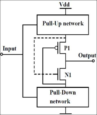
Fig.1. Schematic of LECTOR Method
An inverter circuit is taken as an example to illustrate in detail the Leakage Control Transistor technique. Fig 2 shows LECTOR inverter. The linking drain nodes of LCT1 and LCT2 are taken as the output of the inverter. The LCT2 and LCT1 potential at source control the gates of LCT1 and LCT2 respectively. For any input, one of the two LCTs is always kept near its cut-off region. A voltage of 800mv at the node N2 is observed with vdd=1v and Vin=0. As the voltage is not adequate LCT1 cannot be turned OFF completely. Hence, the LCT1 allows conduction with resistance nearing to it’s OFF. The resistance produced by LCT1 is not identical to the OFF resistance this boosts up the supply to ground resistance, leading to the reduction in sub-threshold leakage current which results in the decrease in leakage power.
The gate propagation delay also increases along with the increase in resistance in the path. The size of transistors is varied in such a way that the delay is cut down or is equivalent to its initial situation. In Lector technique two transistors are included in all paths from supply to ground regardless of the amount of transistors from pull-up to pull-down network. The constant loading necessity with LCTs is seen which is much lesser.
Whereas, the loading necessities with other approaches is large and depends on the number of transistors added. Hence, in case of LECTOR method, the performance degradation is insignificant and overcomes the drawback faced by other techniques [12-14].
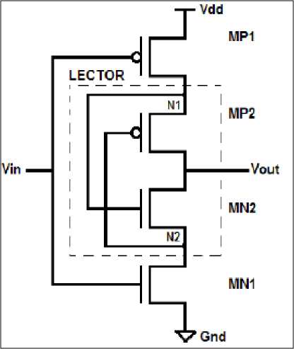
Fig.2. LECTOR Inverter
In the proposed design the full adder circuit is implemented by less number of transistors and the sum output is expressed in terms of carry output. Fig 3 and 4 shows the layout and schematic of Lector based Full adder implemented in cadence virtuoso.
-
B. Magnetic Full Adder
Magnetic Full Adder is used in processors to construct low power high-density arithmetic or logic unit. The MFA circuit in standby mode provides an approximately zero leakage current. However, in the presence of radiation effects, these Magnetic Full Adder circuits cannot assure a fault-free operation [5].
-
C. PCSA Based STT-MFA
The generic STT-MFA structure comprises three parts: a PCSA circuit as shown in Fig 5 that analyses the logic outcome on the outputs, a data block that acts as a logic control and a write logic block to program the STT-MRAM cells. The logic data block consists of a logic tree that is built using MOS device and STT-MRAM [8]. A PCSA circuit comprises of a precharge sub-circuit MP2-MP3, MN2 acts as a discharge sub-circuit which is connected to the clock, and combination of inverters which acts as an amplifier. The circuit operates in two stages. During the first stage, the clock signal is “0” and the outputs “Qm” and “/Qm” are pulled-up to “VDD” through PMOS transistors MP2-3 while NMOS transistor MN2 remains off. At the second stage, “CLK” signal is “1”, the PMOS transistors are turned off and NMOS transistor MN2 turns on.
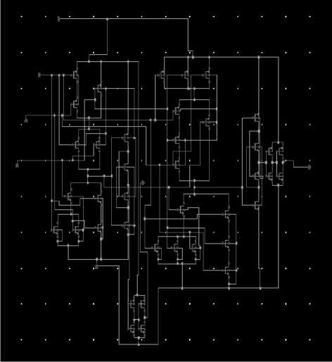
Fig.4.Schematic of a LECTOR based Full Adder
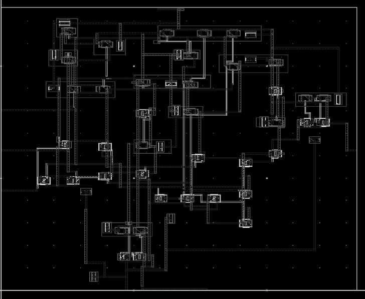
Fig.3. Layout of LECTOR based Full Adder
Discharge currents in the two branches are different, due to the resistance difference between them. To attain the threshold potential of transistor MP1/MP2 the subcircuit with lesser resistance will be pulled-down more quickly, at that instant, the other branch will be pulled to logic “1” or “VDD” and the branch with low resistance will be pulled to “Gnd” or logic “0”. In STT-MFA design the PCSA circuit is used for two purposes: primarily, the ultra-low power magnification from analog data to digital is obtained due to the dynamic sensing; secondly, the read disturbance can be significantly decreased that is induced during sensing operations.
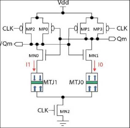
Fig.5. Pre Charge Sense Amplifier
The bidirectional write circuit as shown in Fig 6 is used in this STT-MFA for programming the complementary cells. The circuit consists of two inverters. Every time to generate current either NMOS or PMOS transistors are active, and the other transistors are closed. Write logic implemented by pass transistors are used to program MTJ cells.
The pass transistors are linked to the serial branch's bottom electrodes (BE), top electrodes (TE) and to the common point. These connections are in a way, such that control signal “Input1” / “Input2” is initialized and in the first place device B is laid in high or low resistance state whereas the other device “/B” is placed in the complementary state RP or RAP.
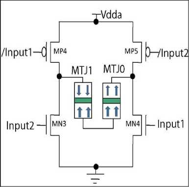
Fig.6. STT Writing Circuit
Fig 7 shows a previous MFA circuit which comprises two sub-circuits one for sum and other for the carry output (Co). The Sense Amplifier (SA) circuit is utilized for reading operation which senses the resistance and configuration related to the MTJs and outputs sum or carry and their compliment output.
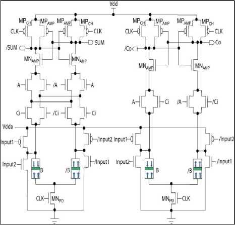
Fig.7. MFA [5]
This is a sequential logic circuit and hence, suffers from Single Event Upset (SEU) caused by radiation.
-
D. Detailed Magnetic Full Adder
Among the three inputs, the input “B” is nonvolatile. To analyze the logic function, PCSA circuit yields the excellent power efficiency and sensing reliability while keeping high-speed performance. Based on the state in the MTJ and logic tree, the discharge current is distinct in both branches and opposite logic value is latched by the sense amplifier. The MOS tree is devised as stated in the truth table of the full adder. For output logic “SUM”, the MOS tree is directly proportional to the inputs “A”, “B”, and “Ci” and logic relationship between them. However, in the logic function due to the presence of the term ACi it is little cumbersome for carry out “Co” logic and the schematic cannot be adapted for the general logic in memory framework. It can be concluded that the outcome of the expression ACi on resistance is exactly identical to the discharging transistor and a sub-branch linking PCSA. The truth table and the formation of resistance of “Co” logic are shown in Table 1. The close and open resistances are respectively RON and ROFF of MOS transistors which is the total resistance of PCSA’s left and right branch. Whatever may be the value of “A” and “Ci” the ACi and /ACi sub-branches have no influence on the output. In case the value of “A” and “Ci” are dissimilar, the two sub-branches resistances are identical. If they are the same, in the condition of ROFF>RAP their comparison corresponds to that of resistance RL and RR, for STT-MRAM which is always true. This yields the term to be removed and achieve the “Co” logic circuit shown in Fig 7.
Table 1. Resistance Configuration of Co
|
A |
в |
Ci |
Resistance Comparison |
Co |
Sub-branch AC, |
Sub-branch |
|
0 |
0 |
0 |
Rl>Rr |
0 |
2Roff |
|
|
0 |
0 |
1 |
R|>Rr |
0 |
RoFF*RON |
Ron* roff |
|
0 |
1 |
0 |
Rl>Rr |
0 |
2R0Ff |
^on |
|
0 |
1 |
1 |
Rl |
1 |
Roff*ron |
ron*Roff |
|
1 |
0 |
0 |
Rl>Rr |
0 |
Ron*roff |
Roff* Ron |
|
1 |
0 |
Rl |
1 |
IRqn |
-Roff |
|
|
1 |
1 |
0 |
Rl |
1 |
ron*roff |
roff* Ron |
|
1 |
1 |
1 |
Rl |
1 |
^ON |
^Roff |
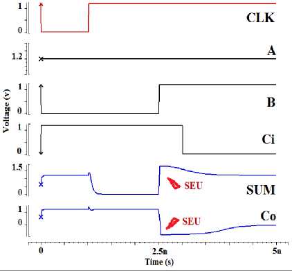
Fig.8. Single Event Upset in MFA
The MFA circuit encounters soft errors caused by radiation because of their CMOS read element. Single
Event Upset injection at output nodes of Magnetic Full Adder circuit is as shown in Fig 8. During the rising edge of the clock the MFA is in evaluate phase, during which an energetic molecule strike in the SA circuits alters the output associated with it to an incorrect state and therefore, they are susceptive to SEUs as well.
Here a radiation-hardened MFA is proposed that is efficient in enduring particle strikes with any amount of charge [8-11].
-
IV. Proposed MFA
The dissimilarity in voltage between the body of the transistor and source results in a change in the threshold voltage (VT) of the transistor this is called body effect. Body bias is a process of connecting the bodies of the transistor to a potential network in the circuit rather than to supply or ground. Body biasing is an approach in which the substrate on the die is biased to some voltage other than GND in case of nmos or Vdd in case of pmos. This technique works to reduce channel sub-threshold leakage. Body biasing is very effective in processes below 65nm as channel leakage is the highest and static power in processes less then 65nm gate leakage is becoming dominant so it is not as much use. Body biasing techniques supervises the body potential of the transistor to modify V t , threshold voltage corresponding to circuits’ requirement. The threshold voltage of a transistor is influenced by various specifications like doping concentration, source to substrate bias, and some other process parameters. Expression 1 shows the dependence of threshold voltage on these parameters:
^t = ^ro + У (VT^fT+^s — VI^PfI) — T]VDS (1)
Where,
Vt0 = Threshold Voltage with zero body bias and which is predominantly dependent on the manufacturing process.
γ = Body Effect Coefficient that depends on the gate oxide capacitance, permittivity of silicon, doping amount and other variables.
Φ F = Surface Potential at threshold.
V SB = Source to Body Voltage.
The consequence of Drain Induced Barrier Lowering (DIBL) is represented by the term ηV DS in which η is the DIBL coefficient [15].
On the whole, fault tolerance is accomplished by biasing at the cost of redundancies causes energy, performance and area overhead. Fig 9 shows the schematic of proposed MFA. In comparison with the previous MFA, in read mode it provides radiation tolerant sensing.
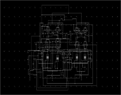
Fig.9. Schematic of Proposed MFA
V. Results and Discussion
The CMOS 45nm technology model and Verilog-A model of MTJ are used in the implementation of the circuits and the circuits are simulated in Cadence Virtuoso. A supply voltage of 1.2V is set in LECTOR adder and in proposed MFA 1V is set. Both the methods are compared and analyzed. Comparison regarding transistor count, input (A, B, Cin) to output (sum and carry) delay, as well as power consumed by two methods is carried out and is as shown in the tabular columns. The truth table of the full adder is as given Table II.
Table 2. Truth table of Full Adder
|
Inputs |
Outputs |
|||
|
A |
В |
Cin |
Stun |
Cout |
|
0 |
0 |
0 |
0 |
0 |
|
0 |
0 |
1 |
1 |
0 |
|
0 |
0 |
1 |
0 |
|
|
0 |
1 |
0 |
1 |
|
|
1 |
0 |
0 |
1 |
0 |
|
1 |
0 |
1 |
0 |
1 |
|
1 |
0 |
0 |
1 |
|
|
1 |
1 |
1 |
1 |
1 |
Fig 10 shows the transient response of the LECTOR based full adder it can be seen that for all the inputs high that output sum and carry is also logic high and when one of the input is zero the outputs sum is zero and carry out is one and also when inputs A, B and Cin are zero both sum and carry outputs are zero.
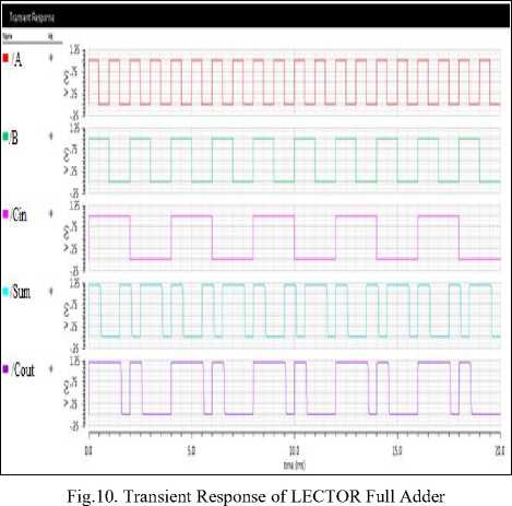
Fig 11 shows the transient response of a proposed Magnetic Full Adder (MFA) from the response it can be that the design is free from Single Event Upset (SEU) error. The Full Adder works with respect to the clock. When the clock signal is high adder is in evaluate state that is the logic operation is performed in this state. When the clock is high and when all the inputs are high the sum and carry outputs are both high, if one of the inputs is zero outputs sum is zero and carry is one and if all the inputs are zero the outputs are zero. When the clock signal is zero adder is in the precharge state. At this state, the outputs are high even if the inputs change
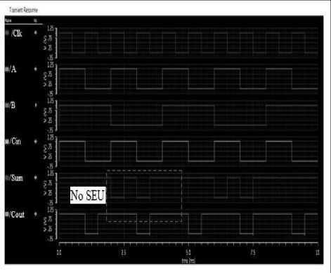
Fig.11. Transient Response of Proposed MFA
Table 3 represents the comparison of Full Adder with their transistor count that gives us data about the area that is larger the count of transistors, larger is the area, and vice versa, delays in terms of each of the inputs to the outputs respectively. Greater the delay, reduced is its operation speed, and vice versa and power dissipation of MFA and Lector methods. It can be seen from the table the proposed MFA is SEU tolerant when compared to the MFA proposed in [5]. And also in Lector method, two methods are achieved that are the transistor count has reduced and the power dissipation has decreased by half when compared to the Lector methods proposed in [14].
Table 3. Comparison Table of Different Parameters of Previous and Proposed Designs
|
Full Adder Circuits |
Number of Transistors |
SEU Tolerance |
Power Dissipation(W) |
Static Power(W) |
Delay from input to Sum (Seconds) |
Delay from input to Cany output(Secon ds) |
|
MFA in [5] |
38 |
No |
In Nano |
Negligible |
||
|
Proposed MFA |
38+8 (Buffets) |
Yes |
5.538ц |
29.95n |
19.18p |
45.47p |
|
Lector in [14] |
53 |
— |
38.50ц |
— |
-- |
|
|
Proposed Lector |
28+8 (Buffers) |
12.61ц |
6.12ц |
637ц (on an average) |
696.3ц(опап average) |
VI. Conclusion
The LECTOR approach has an advantage of not impacting the dynamic power and additionally in this method; less number of transistors are used when compared to the circuit in [14]. The proposed MFA circuit offers SEU tolerance. The proposed MFA circuit consumes less power when compared to the Lector method. To summarize, we can assert that the magnetic full-adder is efficient since the power dissipation in adder circuit is less when compared with the lector technique.
Acknowledgment
I would like to thank the Department of Electronics and Communication, Sri Jayachamarajendra College of Engineering for supporting and encouraging me to carry out this work.
References VLSI implementation of CMOS full adders with low leakage power
- Raju.N,Elamaran.V, Kalagarla Abhiram and Anooj Krishnan, “CMOS VLSI Implementation of Full Adders with Low Leakage Power,” Journal of Applied sciences, 2014.
- Rajesh Mehra, Pushpa R Saini “Leakage Power Reduction in CMOS VLSI Circuits,” International Journal of Computer Applications Volume 55– No.8, October 2012.
- Manoj Kumar, Sandeep K. Arya, and Sujata Pandey, “A New Low Power Single Bit Full Adder Design with 14 Transistors using 3 Novel Transistors XOR Gate,” International Journal of Computer Applications Volume 55– No.8, October 2012.
- Darmala Paradhasaradhi, Sabarish.K, Harish.K, Satya Priya K and G. V. Narasimharao, “Study and Analysis of CMOS Carry Look Ahead Adder with Leakage Power Reduction Approaches,” Indian Journal of Science and Technology, Vol 9(17), May 2016.
- Sina M Bakhtavari, Rajaei Ramin “Ultra-Low Power, Highly Reliable, and Nonvolatile Hybrid MTJ/CMOS Based Full-Adder for Future VLSI Design,” IEEE Transactions on Device and Materials Reliability, 2017.
- Kunjan D. Shinde ,Asha K A, “Analysis, Design and Implementation of Full Adder for Systolic Array Based Architectures – A VLSI Based Approach,” IOSR Journal of VLSI and Signal Processing (IOSR-JVSP) Volume 6, Issue 3, Ver. 2016.
- Raju Gupta, Satya Prakash Pandey, Shyam Akashe, Abhay Vidyarthi “ Analysis and optimization of Active Power and Delay of 10T Full Adder using Power Gating Technique at 45 nm Technology,” IOSR Journal of VLSI and Signal Processing (IOSR-JVSP) Volume 2, Issue 1 2013.
- Erya Deng , Dafine Ravealsona, Jacques Olivier Klein, Claude Chappaert, Yue Zhang, Weisheng Zhao, “Low Power Magnetic Full-Adder based on Spin Transfer Torque MRAM,” IEEE Transactions on Magnetics, 2013.
- Guillaume Prenat, Weisheng Zhao, Klein J. O, Erya Deng, You Wang, Zhaohao Wang, Bernard Dieny, “Robust Magnetic Full-Adder with Voltage Sensing 2T/2MTJ Cell,” IEEE/ACM International Conference Symposium on Nanoscale Architectures, 2015.
- Behtash, Jongayeon Kim, An Chen, Saurabh Kumar, Jian-Ping Wang and Chris H. Kim , “A Technology-Agnostic MTJ SPICE Model with User-Defined Dimensions for STT-MRAM Scalability Studies” Custom Integrated Circuits Conference (CICC), IEEE , 2015.
- Kang.W, Chappert.C, Zhao.W, Deng.E, Ravelosona.D, Cheng.Y, J. Klein, Zhang, “Radiation Hardened hybrid spintronic/CMOS nonvolatile unit using magnetic tunnel junctions,” Journal of Physics D: Applied Physics , 2014.
- Sachin Bandewar, Jyoti Tiwari, “To Reduce the Leakage Power of CMOS Logic Circuit through Lactor Technique,” International Journal of Emerging Technology and Advanced Engineering Volume 5, Issue 11, 2015.
- Venkata Ramakrishna Nandyala and Kamala Kanta Mahapatra, “A Circuit Technique for Leakage Power reduction inCMOS VLSI Circuits,” International Conference on VLSI Systems, Architectures, Technology and Applications.
- Shashank Gautam, “Designing of Full Adder Using Low Power Techniques,” International Journal of Computer, Electrical, Automation, Control and Information Engineering Vol:9, No:4, 2015.
- Pardeep Kumar, Amrita Singh and Susmita Mishra, “Study of Existing Full Adders and To Design a LPFA (Low Power Full Adder),”International Journal of Engineering Research and Applications (IJERA) Vol. 3, Issue 3, May-Jun 2013.
- Fengbo Ren and Dejan Markovi´c, “True Energy-Performance Analysis of the MTJ-Based Logic-in-Memory Architecture (1-Bit Full Adder),” IEEE transactions on electron devices, vol. 57, no. 5, 2010.
- Amit Kumar, Pankaj Srivastava, Manisha Pattanaik “Design of High-speed Power efficient full adder with Body-biasing,” Proceedings of Global Conference on Communication Technologies 2015.
