A Controlled Sinusoidal Signal Generator Based On Direct Digital Synthesize

Author: Liu Zhidong, Wang Shixu, Mao Qun, Xu Zilin, Yang Kuo, Liang Pan
Journal: International Journal of Education and Management Engineering(IJEME) @ijeme
Article in issue: 5 vol.1, 2011.
Free access
In this paper, a controlled sinusoidal signal generator (CSSG) based on the direct digital synthesize (DDS) chip-AD9851 is introduced. The CSSG is controlled by MSP430F4250, which is an ultralow-power microcontroller. The micro control unit (MCU) receives 4-20mA current provided by a current transmitter and then computes the frequency value of the input signal. A frequency value is converted to frequency words which are sent to AD9851. Through an amplifier, a sinusoidal signal can be obtained. With changing the value of input current, sinusoidal signal with different frequency value can be generated. Experiments indicate that the system can produce the sinusoidal signal with frequency 1MHz to 2MHz and accuracy 1Hz.
Sinusoidal Signal Generator, DDS, Current Transmitter, Ultralow-power Microcontroller
Short address: https://sciup.org/15013617
IDR: 15013617
Text of the scientific article A Controlled Sinusoidal Signal Generator Based On Direct Digital Synthesize
Direct digital synthesize (DDS) is a type of frequency synthesizer used for creating arbitrary waveforms from a single, fixed-frequency reference clock. It was proposed firstly by an American scholar J. Tierney, C. M. Rader and B. Gold in 1971[1]. With the development of very large scale integrated circuit technology, DDS technology has experienced a qualitative leap. Now the output waveforms can be up to hundreds of megahertz. DDSs are available in many fields, such as signal generator, medical imaging, wireless, satellite communication, radar, etc [2].
In this paper, a DDS chip-AD9851 produced by the corporation of AD has been introduced to generate sinusoidal wave. And an ultralow-power microcontroller MSP430F4250 produced by the corporation of TI as the CPU controlled the AD9851 and other peripherals. For variable current provided by a high precision current transmitter, sinusoidal wave of different frequency can be generated, with accuracy up to 1Hz. Thus there are many advantages in this system over its high frequency resolution, high converting speed, on line tuning phase, ultralow-power and so on.
* Corresponding author.
2.Fundamental of dds and function of AD9851
-
A. Fundamental of DDS
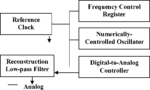
The fundamental mechanism of DDS is presented as below. Firstly, a highly stable reference clock source is used to quantify the sampling interval, samples the generated signal directly with the sampling theorem, makes signal quantization and signal mapping. Then through the D/A controller and low-pass filter, the needed analog signal is obtained [3]. Fig.1 shows the block diagram of the mechanism.
Output
Figure.1. the block diagram of the fundamental of DDS
A stable time for the DDS is provided by the reference clock, and it determines the frequency accuracy of the DDS. At the same time, the reference clock provides the clock to numerical-controlled oscillator. The numerical-controlled oscillator produces a discrete-time, which is quantized version of the output waveform. And the frequency word contained in the frequency control register determines the period of the output waveform. Through the digital-to-analog controller, the sampled waveform is converted to analog waveform. Finally, the spectral replicas produced by the zero-order hold inherent in the analog conversion process are rejected by the reconstruction low-pass filter [4-5].
-
B. Function of AD9851
The AD9851 is a highly integrated device which uses advanced DDS technology, coupled with an internal high speed, high performance D/A converter, and comparator, to form a digitally programmable frequency synthesizer and clock generator function. The functional block diagram is shown in Fig.2.
The features of AD9851 are shown as below:
CD 180 MHz Clock Rate with Selectable 6 x Reference Clock Multiplier.
Key Research Topic of ABA Teachers College (ASA10-15)
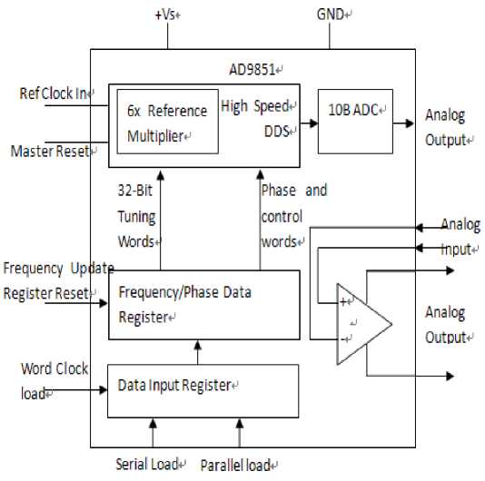
Figure.2. functional block diagram of AD9851
® On-Chip High Performance 10-Bit DAC and High Speed Comparator with Hysteresis
® 32-Bit Frequency Tuning Word
® 5-Bit Phase Modulation and Offset Capability
The relationship between the output frequency, system clock and tuning word of the AD9851 is determined by the expression:
fouт = (kPhase x SystemClock) / 232 (1)
where:
k Phase = decimal value of 32-bit frequency tuning word.
System Clock = direct input reference clock (in MHz) or 6X the input clock (in MHz) if the 6X REFCLK Multiplier is engaged.
f out = frequency of the output signal in MHz.
-
3.Design of hardware and software
-
C. Hardware Design
For the system, an ultralow-power microcontroller MSP430F4250 produced by TI corporation is used as the center to control the whole system, process the data and send the frequency word. The connected block diagram of hardware system is shown as Fig.3.
The XTR105 is a monolithic 4-20mA, 2-wire current transmitter with two precision current sources. It provides complete current excitation for platinum resistance temperature detector (RTD) temperature sensors and bridges, instrumentation amplifiers, and current output circuitry on a single integrated circuit.
The MSP430F4250 features a powerful 16-bit RISC CPU, 16-bit registers, a 16-bit timer, a high performance 16-bit sigma-delta A/D converter, 12-bit D/A converter, 32 I/O pins, a liquid crystal display driver, and constant generators that contribute to maximum code efficiency. The digitally controlled oscillator (DCO) allows wakeup from low-power modes to active mode in less than 6 μs. At the same time, it is convenient to debug on line with the provided JTAG port on-chip.
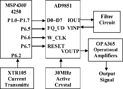
Figure.3. the connected block diagram of hardware system
In Fig.3, the pin P1.0~P1.7 of MSP430F4250 connects the pin D0~D7 of AD9851 as the parallel input port. The Pin P6.5~P6.7 is used to send controlled information respectively to the pin FQ_UD, W_CLK and RESET of AD9851. To ensure that the frequency of output signal is stable and accurate, the system uses 30MHz active crystal as the external clock source.
After power on, the MSP430F4250 initializes the AD9851 and other devices at first. By tuning the potentiometer, the current transmitter sends current to microcontroller. Microcontroller samples the input signal, computes the input data as the frequency words of AD9851, and sends the frequency value to show on the LCD. According the frequency words from the microcontroller, the output signal by pin IOUT is sampled signal, thus, its spectrum includes base frequency and overlapping frequency. For the pure and stable sinusoidal signal output by pin VOUTP, the output signal across external low-pass filter circuit into internal high-speed comparator in AD9851 by pin VINP. The OPA365 is used to amplify the amplitude of output signal. The circuit of amplifier is shown in Fig.4.
-
D. Software Design
For controlling the system and processing data, the software system is necessary. In this paper, we take C programming language of MSP430F4250 to program. The program flow chart is shown in Fig.5.
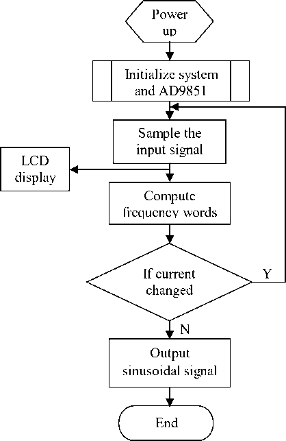
Figure.5. software flow chart
The AD9851 contains a 40-bit register that stores the 32-bit frequency control word, the 5-bit phase modulation word, 6x REFCLK Multiplier enables the power-down function. And this register can be loaded in parallel or serial mode. In this paper, the parallel mode is applied. The frequency of output signal is computed by the formula (1). When the reference clock of AD9851 is 30MHz, the 6x multiplier opened, the frequency of output signal is 1 MHz, and the parallel mode is used, as a programming example for the following AD9851 characteristics:
W0 = 00000001, W1 = 00001010
W2 = 10101010, W3 = 10101010
W4 = 10101010
Figure.4. The circuit of amplifier
In the parallel load mode, the 40-bit input register is loaded using an 8-bit bus. W_CLK is used to load the register in five iterations of eight bytes. The rising edge of FQ_UD transfers the contents of the register into the device to be acted upon and resets the word address pointer to W0. Subsequent W_CLK rising edges load 8-bit data, starting at W0 and then move the word pointer to the next word. After W0 through W4 are loaded, additional W_CLK edges are ignored until either a RESET is asserted or an FQ_UD rising edge resets the address pointer to W0 in preparation for the next 8-bit load. So it is important to pay more attention on the timing sequence.
4.Conclusion
A stable and accurate sinusoidal signal was generated by DDS chip-AD9851 controlled by MSP430F4250. There are many advantages in this system, such as high frequency precision, the stable waveform, frequency adjusted on line, and ultra-low power. However some shortcomings still exists, e.g. there is certain wave spurious signal because of the external crystal connected is an ordinary crystal, the frequency stability is not well enough. So in the future experiment, we will adopt Temperature Compensated Crystal Oscillator for this deficiency. And the low-power filter superior will reduce the performance of the system.
Acknowledgment
This work is supported by the Key Research Topic of ABA Teachers College (ASA10-15).
References A Controlled Sinusoidal Signal Generator Based On Direct Digital Synthesize
- J tiemey, CM Rader, B Gold. A digital frequency synthesizer[J]. IEEE trans, Audio Electroacoust. 1971, AU—19:48—57.
- Shen Gangbao, Teng Gongqing. A pulse generator of DDS based on AD985[J]. Journal of Beijing Institute of Machinery. 2007, 1:116-119.
- Du Huanyang and An Ying, DDS Chip AD9851 and Its Application in Signal Generator [J]. Modern Electronic Technique, 2004, 3:11-12.
- Han Zexi, Zhang Haifei etc. Design of sine wave sign al generator based on DDS technology[J]. Electronic Test. 2009, 8:65-71.
- Cha Wen, Chen Cheng. The Research of SignaI Source on the Basis of Controlled AD9851 [J]. MICROPROCESSORS. 2010,1:116-119.
