A Discussion of a 60GHz Meander Slot Antenna for an RFID TAG with Lumped Element

Author: Omrane NECIBI, Abdelhak FERCHICHI, Tan-phu VUONG, Ali GHARSALLAH
Journal: International Journal of Wireless and Microwave Technologies(IJWMT) @ijwmt
Article in issue: 2 Vol.4, 2014.
Free access
In this paper, a novel approach to design an antenna for a transponder in radio frequency identification (RFID) is proposed. This approach is based on using a meander slot patch with a coplanar waveguide excitation (CPW). The RFID frequency chosen is the free 60 GHz band. The proposed circuit does not require complex package or bonding, thanks to the on-chip antenna, and it does not need battery. This technology is characterized by the low-cost, low-weight and low-area occupation. These particular specifications are important of this micro-RFID, especially if produced in large scale for the mass-market. Since the model of antennas in silicon technology is one of the main challenges, particularly for this proposal. The structure is simulated by using Computer Simulation Technology (CST). The antenna size is 1.95 * 1.99 mm2.This proposed antenna presents again which means a possibility to increase the readable range.
Meander slot Antenna, RFID TAG, micro-RFID, Millimeter wave identification, Lumped element, readable range
Short address: https://sciup.org/15012857
IDR: 15012857
Text of the scientific article A Discussion of a 60GHz Meander Slot Antenna for an RFID TAG with Lumped Element
led to a search for robust and reliable technologies, at relatively reasonable in object identification. Studies developed under the new military and civilian markets were originally an important development of automatic Identifications Systems and led to the emergence of this technology known RFID system. RFID technology has several advantages that can make the identification task faster, efficiently and without contact.
Radio Frequency Identification has been limited to early for military applications at low frequencies. Subsequently, these systems invade different areas of human life such as industrial, education, transportation, medicine, etc.
This technology is based on radio transmission between a reader (also known by a base station controller or interrogator) and transponder (also called smart labels or TAG). The type label identifies the type of system: it speaks of the label passive or active.
Passive tags are the most popular because of their low cost. The identification is performed by tags also called "smart tags" that are associated with objects to be identified. The tag consists of two components: an antenna and an electronic chip. Contrary to active tags that contain power sources, passive tags are powered indirectly from the energy received from the reader.
Reducing the cost and size is the most important point for developers of passive or active RFID tags. This is achieved by using miniaturization techniques for component labels and special materials for their manufacture.
Currently RFID systems operate mainly in the narrow frequency bands around 125 KHz (low-frequency band (LF)), 13.56 MHz (high-frequency band (HF)), 869 MHz (ultra-high-frequency band (UHF)), 2.45GHz and 5.8GHz. Given the increasing number of this type of system, these bands begin to be saturated and it becomes difficult to incorporate new systems. The frequency band around 60 GHz, allowing a spectral width of 7 GHz, is one of possible solutions for the integration of RF devices. This is the solution that is going to Studying in this work.
Indeed, passive micro-RFID tags can be efficiently adopted for a series of new short-range applications such as contact- less cards (e.g. credit or debit card), secure keys (secure automobile or door keys) and they can also be integrated into banknotes in order to increase the security against falsification. The key limitations of these tags are the power consumption and the difficulty to design the system as small as possible preserving a low manufacturing-cost.
We propose in this work, a design of a very small antenna for an RFID TAG with a silicon technology. In the first section, we explained the overall characteristics of the millimeter antenna. In the second Section, we described our design of structure where we present the on-chip antenna; we have also proposed an electrical model to proposed structure. In the last section, we present the simulation results of our on-chip antenna, we conclude our work and we suggest some perspectives.
-
2. General characteristics
-
2.1. Robustness of the antenna
-
2.2. Adaptation of the antenna
The RFID applications are extensive. Inductive RFID systems that used at LF and HF bands are broadly adopted, notably for access control, where short operational range and low data rate are desirable, even acceptable. In recent years [1], the UHF band has also been adopted for RFID. The UHF RFID systems are radio-active, contrary to the near-field-based systems at LF and HF, and they suggest an operational range of a few meters with passive tags low-cost. Microwave frequencies in the 2.45-GHz industrial scientific medical (ISM) band are used also for some applications such as for example monitoring the location of tags because this band with a width of 83.5 MHz sharing frequencies with applications amateur radio and radio service location. These real-time positioning systems generally require an active transponder (with battery).
Evidently, a tendency to move to ever higher frequencies is discussed in this work. Here we propose new concepts which call the millimeter wave frequencies instead of below 3 GHz frequencies typical for RFID. This concept can be called millimeter wave identification (MMID).
There are many benefits of MMID over RFID. At millimeter frequencies, 60 GHz for example, high data-rate (higher than gigabit) communications can be implemented. Here, an attractive application would be battery-less wireless mass memories that can be read in a few seconds with high data rates. Moreover, at millimeter waves, directive antennas are small. A reader device with a small antenna would provide the possibility of selecting a transponder by pointing toward it. This is not possible in today’s UHF RFID systems because directive antennas are too large. A directive reader antenna would help in locating transponders in high-density sensor networks or other places where transponders are densely located. Lastly, there are already applications where millimeter-wave radars are used, as in automotive radars. These radars could, in principle, be used as MMID reader devices that could communicate with the transponders.
There has been some research on RFID at microwaves, at 24 GHz [2], and by the authors at millimeter waves, for example, at 60 GHz [3] and 77 GHz [4]. These papers, however, concentrate just on one component of the MMID system, namely, the conception and realization of a transponder. An MMID system composed of two main constituents: a reader device and a transponder (or tag). The fundamental operation of the system resembles to that of any other RFID system. The reader generally acts master compared to the tag, if the tag is in the reading zone of the drive, the last active by sending an electromagnetic wave and shall initiate the communication.
In the millimeter band antenna is very sensitive to its environment. The approach of a hand or an object can change in a substantial way its characteristic radiation. Such a disturbing result in the case of the antenna impedance by a displacement frequency thereof, the antenna no longer resonates to the same frequency!
We then define the "robustness" of the antenna: Longer antenna is insensitive to variations in the external environment; it is more "robust" millimeter antennas seem less suited to this more problematic than other branches in other bands. This is even more interesting than in most RFID applications, tags are placed on all sorts of different objects.
The adaptation of the antenna of the RFID label is fundamental to the power provided by the reader comes into foot antenna. The figure below illustrates the problem of adaptation.
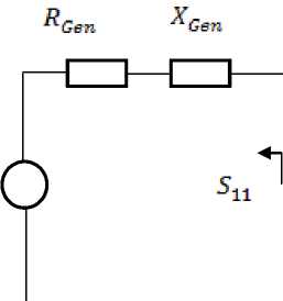
Antenna
Generator
Fig. 1 Equivalent model of a smart antenna system RFID.
^Generator ^G "^ j^G
Impedance of the generator connected to the antenna.
^Gene - (R1osses + ^rad) + J^rad
Impedance of the antenna.
Reflection coefficient of the antenna.
This parameter is important because it defines adaptation. Weaker it is, that is to say the more impedance of the antenna is close to that the reader better will be the adaptation and thus the power transfer between the
7 7
reader antenna and the tag. This is what we seek to achieve in practice: ^ANT tends to “ Generator *
. c
(conjugate) or tends to 0.
The antenna is similar has a complex impedance series. Thus the power that passes into the antenna decomposes into two parts:
-
• Active power (due to the real part of the impedance of the antenna * ^losses * ^radiation ) • Reactive power (due to the imaginary part of the impedance of the antenna * ^radiation ).
As a result to obtain a maximum antenna radiation (i.e.: all the available power is radiated) must:

radiation
p
^losses
+ 0* 0
A loss is due to losses in the conductor (Joule losses) combined with dielectric losses. The use of specific materials will therefore allow reduce it.
Regarding л radiation regardless of the type of antenna used, the resonance implies л radiation и
.
This means that any antenna radiates its resonance an optimal way, so it will be necessary to define the geometry of the antenna way to coincide along with the resonance frequency of the most useful communication tag.
That said, for a question of robustness it is best not to work resonance.
To obtain a perfect power transmission between the reader (Z reader) and tag antenna
7 = (R R + iX •
(■^AVT V*403363 т “radV т V^rad ) it is necessary that the impedances are appropriate, complex
7 —7*
.
impedance is suitable Gen ^ANT
Furthermore, for maximum radiation, it is necessary that R losses and л rad are zero.
. . Y х • • • •• У
So there is a problem: the first condition implies л rad = , while the second condition implies=
0. It is therefore impossible in the RFID application to have a perfect performance antenna except where v
■Л Gen =0.
The compromise used in practice is not imposed л rad = 0, the radiation is thus not perfect (the antenna does not work on resonance but antenna with respect to the environment is gaining strength.
Finally, to achieve high communication ranges, the gain is maximized by making the directional antenna (rated well: Notion directional antenna is not troublesome when one considers that the tag will be detected by readers gill space 3D).
-
3. The proposed on chip-antenna
-
3.1. The Proposed Design
On chip-Antenna become very useful in many applications. Actually, many techniques are used to evaluate these kinds of antenna.
The whole structure is given in figure 2. It’s a multi-layer on-chip-antenna. It consists of a silicon based on-chip feeding structure and one supporting layer. The feeding structure is created by a grounded coplanar waveguide (GCPW) and a meander slot.
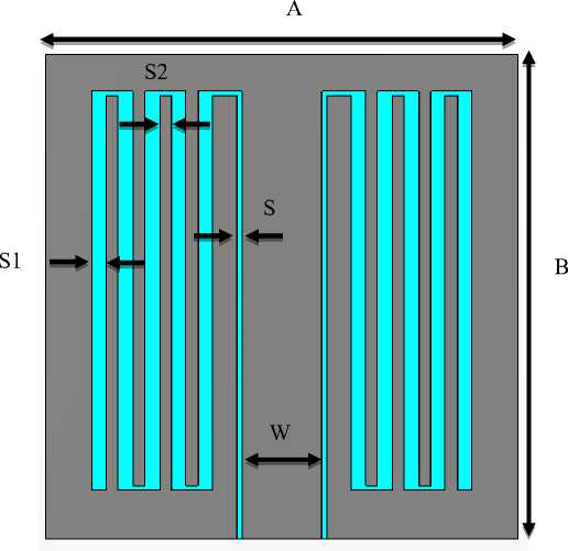
Fig.2 3D on-chip antenna-top-sectional view of the feeding structure (x-y plane), where A =1.95, B =1.99, W=0.33, S =0.019, S1 =0.06, S2 =0.05; (all dimensions in mm).
The meander slot is implemented on the 2µm thick top metal. It is shielded by the bottom metal and connected to a 50Ω-GCPW with a signal line width of w =330 µm and slot width of s = 19 µm.
The CPW (Coplanar waveguide) topology is a good candidate to design the antenna for the 60-GHz microRFID tag. Several studies in the literature [5] have also demonstrated that in HR SOI substrates the losses are strongly reduced if compared with the bulk silicon technology, in which the CPW transmission lines are made only on the top metal layer in order to reduce substrate losses. It is very significant noting that the ground planes have to be large enough to introduce negligible effects on the antenna property, and then a compromise has been reached between infinite ground planes and suitable dimensions for silicon applications.
To ameliorate on-chip antenna performance, several techniques including high resistivity silicon substrate, micro-machining, and artificial magnetic conductor concept have been reported. These techniques [6-7-8], however, had limited antenna gain of less than 14 dBi, and some indicate the significance fabrication process complexity and design difficulty. A dielectric lens-based on-chip antenna [9] and an on-chip horn antenna [10] have pushed the radiation efficiency of 60% and the gain up to 8 dBi. These techniques, however, required external back end of line (BEOL) processes and occupied relatively large chip area.
With the advancement of low-cost silicon technology, interests in silicon-based wireless system-on-chip (SOC) applications have become pervasive [11], [12]. On-chip antennas eliminate the need for external off-chip connection and packaging process which would incur a gain loss and overall size increase [13].
Metal
SiO2
Si

Fig.3 Geometry of the proposed antenna (Button view).
"Above-IC" technology is to refer to the silicon dioxide layer Silicon (SiO2) or other dielectric thin in order to see the radiating element and the mask largely lossy silicon substrate. This solution is interesting because it is compatible with low-cost millimeter integration.
We explored on-chip antenna based on the meander slot antenna. This simple antenna has historically been very reliable and provides reasonable gain, high front-to-back and front-to-side ratios, and radiation near the horizon.
The layer of silicon dioxide under metal layer is modeled as lossless, while the losses in silicon substrate are modeled with conductivity (σ) of 10 Sm-1, as in [14] and in [15]. Realistic millimeter wave antennas were modeled with CST, a leading commercial finite element method field solver which simulates three-dimensional structures and produces S-parameters and radiation patterns. The effective wavelength at 60 GHz for an IC substrate is estimated by using the frequency and material properties of the top IC layer (silicon dioxide, = 3.9), where
^"freespace
Vе dM (4)
-
_ 1 __ ^-freesp ace
-
3.2. The Proposed electrical model for the on-chip antenna
<Eosr^of ^ (5)
Where ^freespace is 5 mm for 60 GHz and, ^■effective is calculated by including the effect of the dielectric constant. Here, ^effective = 2.53 mm.
In order to determine the geometry parameter of each our antenna, we build an electric model for the proposed configuration, Fig.4.
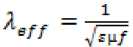
We build the electric model by analogy to a classical meander antenna. The values of the parameters of the circuit are calculated from the geometry parameters of our antenna.
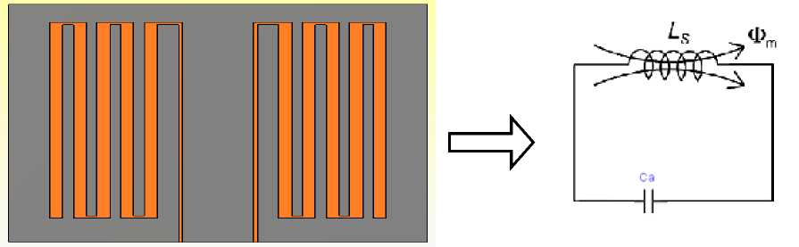
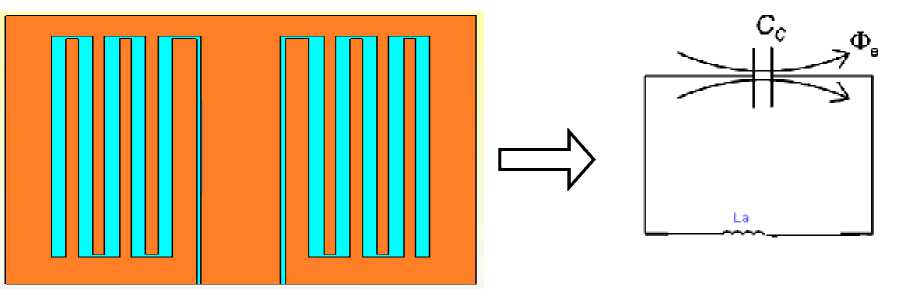
Fig.4 The electrical model of the On-Chip-antenna.
The meander slot element consists of horizontal and vertical slot so it formed a series of sets of right angled bends. The polarization of the antenna depends on radiations from the bend. The spacing between two bends is very important, where if the bends are too close to each other, then cross coupling will be more, which affects the polarization purity of the resultant radiation pattern.
In another case the spacing is limited due to the available array grid space and also the polarization of the radiated field will vary with the spacing between the bends.
The electrical small antenna is defined as the largest dimension of the antenna is no more than one-tenth of a wavelength. The meander Slot antenna is electrically small antenna .The design of meander Slot antenna is a set of vertical and horizontal slot. Combination of vertical and horizontal Slot forms turns. Number of turns increases efficiency increases. In case of meander slot if meander spacing is increased resonant frequency decreases. At the same meander separation increase resonant frequency decreases.
-
3.3. Result of Simulation
This section presents the simulated results of the meander slot antenna. CST has been used to simulate the antenna.
The parametric study of the antennas reveals the band behavior. The antenna is conceived to operate on 60 GHz free bands. Fig.5 illustrates the S11 of antenna; where it shows a return loss of -42.92 dB for the operation of 60 GHz.
The impedance bandwidth calculated at -10 dB scale for this band is 450 MHz with a tag antenna gain (GTAG) of 3.47 dBi the value which determines the operating range, is about 15 cm. The area needed for the antenna design is roughly 2 mm2, compliance with on-chip realization.
Fig.5 Simulated reflection coefficient for the On-Chip antenna.
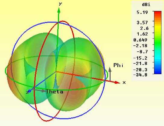
Fig.6 Simulated directivity of the proposed antenna.
The simulated current distribution on the Surface of Meander slot antenna is presented in Fig.7. The ground plane in small antennas plays a major role in radiation. For example the change in the size of ground plane creates a shift in the resonant frequencies. The current distribution on the ground plane and its effect on the resonant frequencies were also observed during simulation.
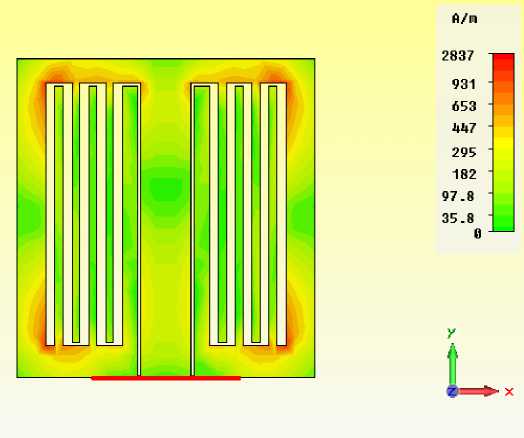
Fig.7 Surface current distribution on antenna at 60 GHz.
-
4. Conclusion
In this work, design of a single element antenna system operating in the free frequency band was presented due to size reduction proposed antenna useful for RFID communication. The On-Chip-antenna for an RFID TAG operates in the 60 GHz frequency band with a bandwidth is 450 MHz .Return loss is - 42.92 dB is obtained. The proposed research and discussion presented in this work are meant to provide an intuitive point of view on the fundamental requirements regarding the RFID antenna and millimeter wave identification.
References A Discussion of a 60GHz Meander Slot Antenna for an RFID TAG with Lumped Element
- K. Finkenzeller, RFID Handbook, 2nd edition. New York, Wiley, 2003.
- E. M. Biebl, “RF systems based on active integrated antennas,” Int. J. Electron. Commun. (Arch. Elektr. Ubertragung), vol. 57, no. 3, pp. 173–180, 2003.
- A. Müller, D. Neculoiu , M. Dragoman, D. Vasilache, I. Petrini, G. Konstantinidis, C. Buiculescu, Z. Hazoupulos, A. Stavinidris, T.V?h?-Heikkil?, N. Kornilios, L. Bary, P. Pursula, D. Dascalu, and R. Plana, “GaAs membrane-supported 60 GHz receiver with Yagi–Uda antenna,” in Proc. 8th Int. RF MEMS RF Micro-system Conference, MEMSWAVE 2007, Barcelona, pp. 15–18, Jun. 26–29, 2007.
- A. Müller, P. Pursula, D. Neculoiu, F. Giacomozzi, J. Tuovinen, and T. V?h?-Heikkil?, “Hybrid integrated micro machined receiver for 77 GHz millimeter wave identification systems,” in 37th European Microwave Conference., Munich, Germany, pp. 1034–1037, Oct. 2007.
- F. Gianesello, D. Gloria, S. Montusclat, C. Raynaud, S. Boret, C. Clement, G. Dambrine, S. Lepilliet, F. Saguin, P. Scheer, P. Benech, J.M. Fournier, "65 nm RFCMOS technologies with bulk and HR SOI substrate for millimeter wave passives and circuits characterized up to 220 GHz", IEEE MTT-S International Microwave Symposium Digest, pp. 1927 – 1930, 11-16 June 2006.
- P. V. Bijumon, A. P. Freundorfer, Y. Antar, and M. Sayer, “Dielectric resonator antenna on silicon substrate for system on-chip applications,” IEEE Transaction Antennas & Propagation, vol. 56, no. 11, pp. 3404–3410, Nov. 2008.
- E. Ojefors, E. Sonmeza, S. Chartier, P. Lindberg, A. Rydberg, and H. Schumacher, “Monolithic integration of a folded dipole antenna with a 24-GHz receiver in SiGe HBT technology,” IEEE Transaction Microwave Theory Tech., vol. 55, no. 7, pp. 1467–1475, Jul. 2007.
- E. Ojefors,H. Kratz, K.Grenier, R. Plana, and A. Rydberg, “Micro machined loop antennas on low resistivity silicon substrates,” IEEE Trans. Antennas Propag., vol. 54, no. 12, pp. 3593–3601, Dec. 2006.
- K. Kang, F. Lin, D. D. Pham, J. Brinkhoff, C. H. Heng, Y. X. Guo, and X. Yuan, “A 60-GHz OOK receiver with an on-chip antenna in 90 nm CMOS,” IEEE J. Solid-State Circuits, vol. 45, no. 9, pp. 1720–1731, Sep. 2010.
- A. Babakhani, G. Xiang, A. Komijani, A. Natarajan, and A. Hajimiri, “A 77-GHz phased-array transceiver with on-chip antennas in silicon: Receiver and antennas,” IEEE J. Solid-State Circuits, vol. 41, no. 12, pp. 2795–2806, Dec. 2006.
- K. K. O. et al., “On-chip antennas in silicon ICs and their application,” IEEE Transaction Electron Devices, vol. 52, no. 7, pp. 1312–1323, Jul. 2005.
- B. Razavi, “Design of millimetre-wave CMOS radios: A tutorial,” IEEE Transaction Circuits Syst. I, Reg. Papers, vol. 56, no. 1, pp. 4–16, Jan. 2009.
- Y. C. Ou and G. M. Rebeiz, “On-chip slot-ring and high-gain horn antennas for millimeter-wave wafer-scale silicon systems,” IEEE Transaction Microwave Theory Tech., vol. 59, no. 8, pp. 1963–1972, Aug. 2011.
- Y. Zhang, M. Sun, and L. Guo, “On-chip antennas for 60-GHz radios in silicon technology,” IEEE Transaction Electron Devices, vol. 52, no. 7, pp. 1664–1668, July 2005.
- D. H. Neil H. E. Weste, CMOS VLSI Design, 3rd edition. Addison Wesley, 2004.
