A New High-Performance Bridge Structure for 4-to-2 Compressor using CMOS and CNFET Technology

Author: Mehdi Darvishi, Mehdi Bagherizadeh
Journal: International Journal of Modern Education and Computer Science (IJMECS) @ijmecs
Article in issue: 6 vol.9, 2017.
Free access
In this paper, a new high-speed and energy efficient 4-to-2 compressor cell was presented using carbon nanotube field effect transistors (CNFETs). CNFET is very suitable for high-frequency and low-voltage applications. In addition, in this paper several conventional and state-of-the-art 4-to-2 compressor cells are surveyed and compared. In order to evaluate the proposed designs, computer simulations are carried out using 32nm-CMOS and 32nm-CNFET technologies. Simulations are conducted using various low voltage power supplies, different temperatures, frequencies and load capacitors. Results of simulation demonstrate predominance of the proposed design in terms of power consumption, delay, and power-delay product (PDP) compared to other 4-to-2 compressor cells and they confirm that the proposed design is the fastest 4-to-2 compressor in various working circumstances.
Carbon Nanotube Field Effect Transistor, CNFET, 4-to-2 Compressor, Compressor, Nanotechnology
Short address: https://sciup.org/15014979
IDR: 15014979
Text of the scientific article A New High-Performance Bridge Structure for 4-to-2 Compressor using CMOS and CNFET Technology
Published Online June 2017 in MECS
Todays' need of designing large-scale, high-speed and low-power integration (VLSI) circuits has been increased extremely. However, there are a number of problems in the technology of scaling metal oxide semiconductor field effect transistors (MOSFETs). Problems like drain-induced barrier lowering effect, leakage current, and other short channel effects degrade the performance of VLSI circuits [1]. In other words, with scaling down of the feature size in nano ranges, MOSFET technology has faced significant challenges including high sensitivity to process variations, decreased gate control, high-power densities, and short channel effects [2, 3]. Actually scaling becomes a difficult task when thinking to shrink their sizes more and more. Difficulties related to system efficiency and manufacturing technology.
Many solutions have been proposed by experts to fix this problem. One of the solutions to overcome these problems is carbon nanotube field effect transistors (CNFETs) technology [4, 5]. Due to the similarity between MOSFETs and CNFETs in terms of natural features and operation, CNFET appears to be more promising and practical compared to other nanotechnologies [5]. A carbon nanotube field effect transistor has a carbon nanotube, which could be a single nanotube or a nanotube array. In nature, nanotubes are stationary and could carry a high electric current [4]. One of the remarkable characteristics of CNFET is that N-CNFET and P-CNFET, with the similar device geometries. These transistors have the same mobility and identical current drive capabilities, which is very important for transistor sizing in intricate circuits [6].
Multiplication is the most important arithmetic operation in many applications executed on common and specific purpose digital processors. A multiplication process consists of three phases: partial product generation, partial product reduction, and the final carry propagating addition. The most area consuming and power dissipating part among aforementioned three phases is partial products reduction. This phase has received a lot of attention by researchers of digital multipliers [7, 8].
In multiplication hardware and multi-operand addition, compressor cells seem to be the most generic bit-compressing cells with main application. Digital multiplication circuits are used extensively in digital signal processors and microprocessors. Performance of many arithmetic algorithms depends on multiplier’s efficiency [9]. Due to the critical role of compressor cells in the design of efficient multipliers, the comprehensive study of design alternatives of these cells was motivated. Compressor cells are used in multiplier circuits in order to reduce the number of partial products. The advantages and performance of compressor cells are understood via gate level analysis. The real implementation of these cells is based on the final figs of merits namely area, delay, and power consumption [10, 11]. In this paper, new 4-to-2 compressor cells are presented using a novice method. The new design based on new interpretation of compressor cell functionality, all with the goal of increased efficiency. The efficiency of 4-to-2 compressor cells is exclusively influential on performance of multiplication computations [12]. A 4-to-2 compressor is functionally equal to two cascaded Full Adders (FAs) [9, 13]. The structure of compressor could be of more interesting using the CNTFET technology. Therefore, in this paper a new designing method for 4-to-2 compressor cells is introduced using CNTFET technology. The efficiency of our proposed 4-to-2 compressor cell has been thoroughly checked under different frequencies, temperatures, voltage supply and load capacitors.
In the rest of this paper, a brief review of carbon nanotube field effect transistors is presented in section 2. In section 3, recently reported compressors' architectures and literature are reviewed. Section 4 introduces our proposed CNFET-based 4-to-2 compressor cell, while the corresponding simulation results and comparisons for 4-to-2 compressor cells are offered in Section 5. Finally, Section 6 presents the conclusions.
-
II. Carbon Nanotube Field Effect Transistors (CNFETS)
To generate smaller chips, scalability is applied which has led to challenges in MOSFET characteristics [11], since researchers pursue an appropriate replacement for MOSFET technology. Results of elementary experiments conducted on semiconductor single walled CNFETs demonstrate equivalent manner like that of MOSFETs. CNFET technology is qualified to become an appropriate replacement for MOSFET at nanoscale, due to the good electric attributes of this technology, including timely switching and acceptable current- voltage conversion [11, 14, 15]. With respect to that of MOSFET, these transistors have high-speed and low-power consumption. Another advantage of CNFET is its appropriate function at low-input voltages [11]. Actually, carbon nanotube (CNT) is a sheet of graphite that is rolled up along a wrapping vector [16]. CNTs have appropriate features such as ballistic convey of electrons along the tube and a simple construction process. These features make them appropriate for designing CNFETs [17]. CNTs are classified into two categories: single-wall CNTs (SWCNTs) and multi-wall CNTs (MWCNTs). SWCNTs are composed of one cylinder while MWCNTs have more than one cylinder [17]. Each CNT has a specified vector called chirality, which is defined as ch = na 1 +ma 2 : where, (n, m) are chiral numbers and (a 1 , a 2 ) are unit vectors [11]. SWCNTs could be conducting or semiconducting, in order to the relationship between (n, m) in chiral vector [18]. If n-m = 3k(k e z) , CNT is metallic, otherwise is semiconductor[18].
Semiconducting SWCNTs can be applied as the channel of CNFET device [17]. The width of a CNFET gate can be nearly computed according to (1) [19].
W gate « Min ( W min , N x Pitch) (1)
Where, N is the number of nanotubes under the gate and W min is the minimum width of the gate. The distance between the centers of two adjoining SWCNTs under the same CNFET gate is called pitch, which directly affects width of the gate and contacts of the device [5]. One of the most advantageous features of a CNFET device is that the appetence threshold voltage can be adjusted by adopting appropriate diameter for its CNTs [17]. This feasible characteristic makes CNFET more flexible than MOSFET for designing digital circuits and makes it very appropriate for designing multi-threshold circuits [5].The threshold voltage of CNFET is computed by (2) [17].
V th =
a 0 V p D CNT(nm)
0.436
D CNT(nm)
Where, a 0 ( 0.142 nm) is the length of carbon-to-carbon bond in a CNT [17], V p 3.033 eV the carbon П — П bond energy in the tight bonding model, and e represents the electric charge of a single electron [20]. Dcnt is the diameter of its nanotube which is computed by Equation (3) [17].
V3 a о V n 2 + nm + m 2 x
D cnt =-------------------- (3)
π
Where, 3a0 is the distance between carbon atoms,nU 3.033eV is the carbon п—П bond energy in the tight bonding model, and n and m chiral numbers [11]. In the literature, three different types of CNFETs have already been presented, namely SB-CNFET, T-CNFET and MOSFET-LIKE CNFET [17]. SB-CNFET is a tunneling device. This device works on the tenets of direct tunneling by a schottky Barrier at the source channel intersection [5]. SB-CNFETs indicate strong ambipolar specifications that restrict the application of these devices in CMOS-like logic families. This kind of CNFET is suitable to moderate high-efficiency applications [5].
Due to more correspondence with MOSFET in terms of physical characteristics and device structure, MOSFET-LIKE CNFET is more suitable for circuit designing according to CMOS architectures [17]. The third kind of CNFET is called the band-to-band tunneling CNFET (T-CNFET). This kind of CNFET has low ON currents and high cut-off characteristics. T-CNFET is very appropriate for low-power and subthreshold circuit designing [21]. In addition, another important characteristic of CNFET, which makes it more promising, is its unique one-dimensional band structure which suppresses backscattering and causes near-ballistic operation [3]. Chirality of a CNT is the angle difference between grapheme strip’s orientation and axis of the resulting nanotube. Chirality of CNTs affects their semiconducting behavior [4]. In general, CNFET has a higher performance and lower power consumption compared to silicon-based MOSFET and it is very suitable for low-voltage and high-frequency applications [5].
-
III. Relted Works
There are different designs of 4-to-2 compressor cells which have been proposed in various literature [10, 12, 22-25]. In this section, several CMOS and CNFET-based 4-to-2 compressor cells are briefly reviewed. The conventional 4-to-2 compressor cell is shown in Fig.1. This compressor cell has 64 transistors using CMOS implementation of basic blocks. The conventional 4-to-2 compressor cell has a higher noise margin compared to other designs.
Another CMOS 4-to-2 compressor design is shown in Fig.2a [10]. This design is based on (4) and (5). In this design, one full adder and four NAND gates are used on two-input XNOR. The performance of this compressor cell depends on the full adder used in this cell [25].
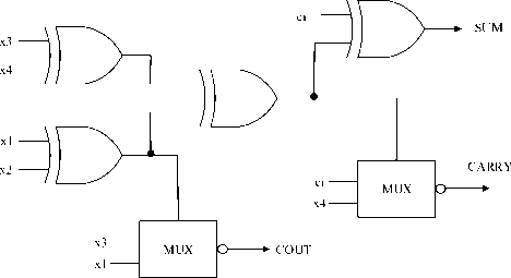
Fig.1. Conventional Compressor Design.
SUM = ( X 40 C i )□ ( X 1 ® X 2 ® X 3 ) (4)
COUT = ( X 1 ® X 2 ® X 3 )( C i ® X 4 ) + ( X 4 C i ) (5)
The CMOS 4-to-2 compressor design in [24] is shown in Fig.2b. The critical path delay of this cell equals the sum of delays of one NAND and two 2-way XNOR and one 2-way XOR gate. There are 72 transistors in this compressor cell.
Another CMOS design shown in Fig.2c has 70 transistors [22].The functionality of this design is based on (6), (7) and (8). The critical path of this cell is about three 2-way XOR gates [25].
SUM = ( X Ш X 2 ) ® ( X 3D X 4 ) ® C i (6)
COUT = (C 1 + C 2 )C 3 (7)
C o = (C 1 C 2 ) (8)
The 4-to-2 compressor design is shown in Fig.2d. The critical path delay of this structure equals the sum of delays of one 2-way XOR, two 2-way XNOR, and two 2-way NAND gates. To design this cell, 78 transistors are required using CMOS implementation of basic blocks [25].
CMOS 4-to-2 compressor design in [12] which is shown in Fig.2e focuses on gate decomposition to employ less transistors [26]. In this design, by decomposition of four XOR gates to three simple gates, eliminates excess of five gates in total of cell. The critical path delay of this cell equals the sum of delays of three NOR and three NAND and one NOT gate. In this cell, the critical path at output nodes is very long which leads to long propagation delay [25]. This design has 74 transistors. The CNFET design in [25] is shown in Fig.2f. In this design, in pull-down and pull-up networks, transistors with normal threshold are used which are controlled by NOT gate with different threshold voltages. To design COUT output, a gate level of a multiplexer cell and a majority function are used. All transistors in the multiplexer cell are of normal threshold [25]. Another CNFET 4-to-2
compressor cell is designed in [27]. This design is highly dependent on diameters of CNT. Accordingly, it is highly sensitive to process and voltage variations.
-
IV. Proposed 4-To-2 Compressor Cell
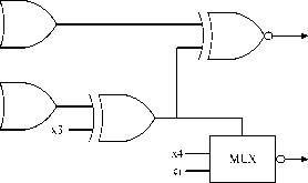
In this section, a new structure is designed for a 4-to-2 compressor. The proposed design is implemented based on CNFET bridge style. In fact, the proposed structure module has advantages of the bridge style including simplicity of the design and low-power consumption. This design offers significant performance improvement compared to an exact 4-to-2 compressor in terms of power consumption, delay, PDP, and the number of transistors [28]. The proposed compressor cell shown in Fig.5, is composed of three separate fully symmetric CNFET pass-transistor networks to implement the SUM and COUT and CARRY outputs in a parallel manner. The first network is a 3-input XOR circuit, which implements the COUT output using 10 CNFETs based on bridge structure and a NOT gate to convert to COUT. The functionality of proposed 4-to-2 compressor cell is based on (9) - (13).
COUT = (X1 • X2 • X 3) + (X1 • X2) + (X2 • X3)
S = ( COUT • X 3 • COUT ) + ( COUT • X 1 ) + ( X 2 • COUT ) + ( X 2 • X 3 • X 1 )
CARRY = (X4• Ci • S) + (Ci • S) + (X4• Ci)
S1 = (X 4 ® Ci)(12)
SUM = ( S I ® S )
-
(13) in detail.
-
A. Bridge Structure
In the following, the proposed structure is discussed
(a)

x4
xx12
SUM
COUT
(b)
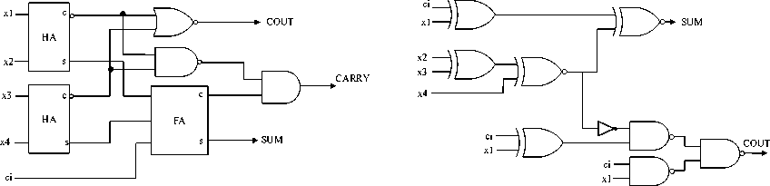
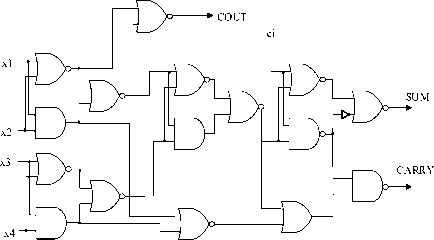
Fig.2. (a) CMOS design [10], (b) CMOS design [24], (c) CMOS design [22], (d) CMOS design [23], (e) CMOS design [12], (f) CNFET design
Bridge structures are circuits that create a conditional connectivity between two circuit nodes. Using this type of structure, the classical VLSI circuits can be designed smaller and faster than the conventional method. One of the important parameters in circuit design is the chip area. Therefore, the bridge structure might increase density or reduce the area of transistors in unit of area [29]. For instance, implementation of the majority function using bridge structure is illustrated in Fig.3.
Majority function could be implemented via a fully symmetric style using bridge structure. Majority are given in figure as the (14).
Majority ( A, B , C ) = ( A • C + B • C + A • B ) (14)
Based on above information, it can be said that the bridge structure could be able to design VLSI circuits in a symmetric manner, which is very advantageous for VLSI layout design, placement and routing. This development can be design mentioned circuits in smaller area [29].
-
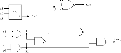
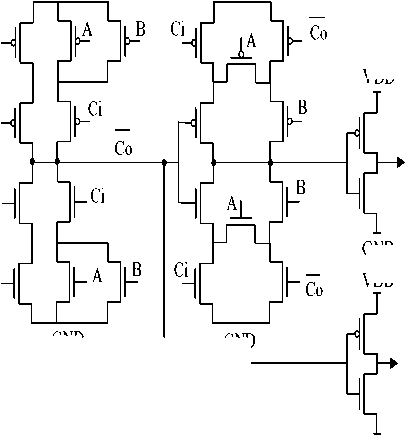
B. Bridge Structure Full Adder
The significant advantage of bridge structure for circuit designing is low number of transistors, its simplicity and modularity. In fact, structure of the bridge by shortening the route and reducing the transistors, reduces the complex and increases the efficiency of proposed 4-to-2 compressor cell [29-31]. Fig.4 shows a full adder cell designed using bridge structure. This bridge design of full adder performs realizations by organizing some different branches.
A
B
A
B
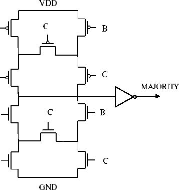
Fig.3. Bridge implementation of majority function (fully-symmetric style).
VDD
VDD
A
VDD
VDD
SUM
COUT
GND
GND
GND
Fig.4. Bridge full adder [29-31].
GND
Bridge design style centralizes its attention on meshes and connects each two adjacent meshes by a transistor, called bridge transistor; whereas each branch provides a path from supply lines to an output [30]. The functionality of the presented Full Adder cell is based on (15) and (16).
COUT = ( A • B + A • C i + B • C i ) (15)
SUM = (C i • A • B + C i • Co + Co • B + Co • A • Co ) (16)
Bridge transistors create a new path from supply lines to an output to provide the possibility of sharing transistors of different paths. Variants of logic circuits can be easily realized with respect to high flexibility of bridge methodology. The bridge transistors must be arranged such that they not only validate the accuracy of the circuit, but also keep pull-up and pull-down networks mutually exclusive. In general, bridge structure can lead to highly structured designs. In this structure, control signals can be applied to the sides of meshes. With respect to the high flexibility of bridge methodology, variants of logic VLSI circuits can be easily realized.
-
C. New 4-to-2 compressor design based on CNFET bridge structure
In the proposed design, two-input XOR gates, three not gate, one bridge structure, and one bridge full adder circuit are used. The XOR gate structures has a low number of transistors with very low power consumption. In the proposed design of 4-to-2 compressor, all three outputs were achieved using a bridge structure Fig.3 Two outputs, SUM and CARRY, are obtained concurrently. This is the most efficient way to reduce delay and power consumption at the same time.
In fact, in some digital computing systems, the basic cell is the compressor which has five inputs (X1, X2, X3, X4 and Ci) and three outputs (SUM, COUT and CARRY). Fig.5 depicts a schematic of proposed 4-to-2 compressor. The proposed compressor cell has a symmetric structure which leads to more simple layout process. This structure has totally 44 transistors. Fig.6 depicts the final structure of proposed 4-to-2 Compressor.
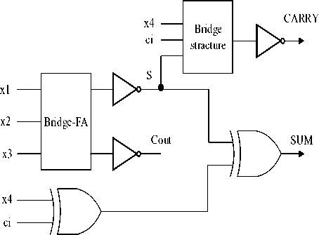
Fig.5. A schematic of proposed design.
The proposed design of 4-to-2 compressor is quite different from the previous structures and it highly outperforms them. This design is completely based on bridge structure. Compared to other designs fewest number of transistors are used. The proposed method to design a 4-to-2 compressor is a super high-speed design and has a very good performance compared to all designs offered up to now.
-
V. Simulation Results
In this section, the proposed designs are evaluated comprehensively in various situations and are compared with other classical and state-of-the-art CMOS and CNFET-based 4-to-2 compressor cells. All designs are simulated using Synopsys HSPICE 2008 simulator tool with 32nm-CMOS technology for CMOS circuits and 32nm-CNFET technology for CNFET-based circuits. Results of this simulation are used to compare the performance of proposed compressor to the performance of other classical and state-of-the-art CMOS and CNFET compressors simulated using Stanford comprehensive
CNFET SPICE model which is described in [32] and using the post-layout CMOS library of standard cell. This standard model has been designed for enhancement-mode unipolar MOSFET-like CNFETs, where each transistor may contain more than one CNT as its channel.
All structures of 4-to-2 compressor cells are simulated using 32nm technology. Maximum delay has been considered as the delay of circuit. To measure cell delay, all possible transitions have been generated through test patterns and it is applied for all structures.
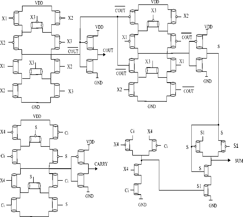
GND
Fig.6. The structure of proposed 4-to-2 compressor.
Simulations are carried out at room temperature and various supply voltages, frequencies and loads are used for it. We provide simulation results of delay, power consumption, and PDP in 27oC with the 0.65V supply voltage, in frequency of 100MH and 2.1fF load capacitor based on MOSFET technology.
In the simulation, CMOS design of [10] Fig.2a, CMOS design of [24] Fig.2b, CMOS design of [22] Fig.2c, CMOS design of [23] Fig.2d, CMOS design of [12] Fig.2e, CNFET design of [25] Fig.2f, and the proposed design, Fig.6, in MOSFET technology are surveyed. Results of this simulation is shown in Table 1. Based on this table, it is clear that the proposed design consumes less static power, less delay and the best PDP among other designs. The best results at each parameter are demonstrated with bold-faced numbers.
According to experimental results, the proposed design has the shortest delay, power and the lowest PDP compared to the other designs in MOSFET technology. In another experiments, all circuits are simulated at 0.65 V power supply, 27°C and at 100MH operating frequency with 2.1fF output load capacitance in CNFET technology [25].
Table 1. Simulation results in 27○C with the 0.65V in frequency 100MH and c-load 2.1fF with MOSFET technology.
|
Compressor Designs |
Delay (×10-10s ) |
Power (×10-7w ) |
PDP (×10-17j ) |
|
CMOS-Design [23] |
118.40 |
1.7496 |
207.14 |
|
CMOS-Design [24] |
19.718 |
2.0368 |
40.160 |
|
CMOS-Design [22] |
101.32 |
1.8027 |
182.65 |
|
CMOS-Design [12] |
19.950 |
2.3500 |
46.883 |
|
CMOS-Design [10] |
24.592 |
1.6182 |
39.794 |
|
CMOS-Proposed Design |
0.97904 |
18.522 |
18.134 |
Here, all MOSFET designs turned into CNFET, and we proved that the proposed in comparison with all designs. In addition to MOSFET technology, in CNFET technology also has full superiority. Results of this experiment are listed in Table 2. Experimental results indicate that the proposed design again has the shortest delay, lowest power consumption and lowest PDP compared to other designs at all parameters.
Table 2. Simulation results in 27○C with the 0.65V in frequency 100MH and c-load 2.1fF with CNFET technology.
|
Compressor Designs |
Delay (×10-10s ) |
Power (×10-7w ) |
PDP (×10-17j ) |
|
CNFET-Design [23] |
100.38 |
159.43 |
16004 |
|
CNFET-Design [24] |
0.42365 |
1.6606 |
0.70352 |
|
CNFET-Design [22] |
100.31 |
1.5632 |
156.81 |
|
CNFET-Design [12] |
100.33 |
1.7675 |
177.34 |
|
CNFET-Design [10] |
0.42579 |
1.3956 |
0.59425 |
|
CNFET-Design [25] |
0.69403 |
8.7052 |
6.0417 |
|
CNFET-Proposed Design |
0.27851 |
1.3594 |
0.37862 |
As shown in these tables, the proposed design has the lowest delay, power consumption and PDP in comparison to other circuits. In the next section, superiority of the proposed design over other designs will be examined comprehensively.
-
A. Temperature Analysis
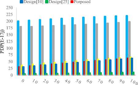
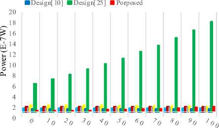
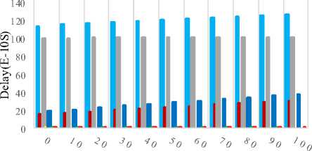
In temperature analysis, circuits are simulated in a wide temperature range of 0–100°C with 0.65V power supply, 2.1fF load capacitor and 100MH frequency. Simulation results for delay, power and PDP are shown in Fig.7, respectively [10]. Simulation results show that the proposed design is consistently faster, consume less power, delay and PDP optimized than the reference designs [10].
Design[23] Design[24] Design[22] Design[12]
Temperature (°C) (a)
Design[23] Design[24] Design[22] Design[ 12]
Temperature (°C) (b)
Design[23] Design[24] Design[22] Design[12]
Design[ 10] Design[25] Porposed
Temperature (°C) (c)
Fig.7. PDP (a) power consumption (b) and delay (c) vs. temperature.
In particular, the delay, power consumption, and PDP plotted in Fig.7 from 0°C to 100°C in order to achieve lowest delay, power consumption, and PDP. Simulation results also show robustness of the proposed circuit against temperature variations.
-
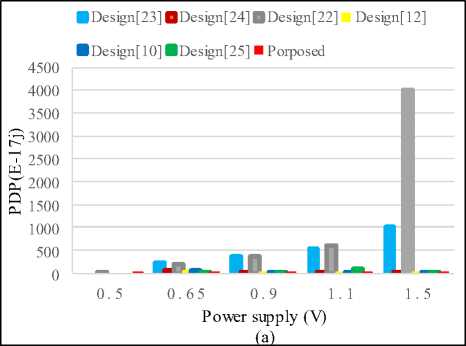
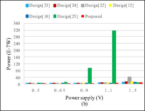
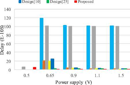
B. Power Supply Analysis
Fig.8 shows simulation results for the studied circuits in a wide voltage range of 0.5–1.1V, based on constant temperature of 27°C, 2.1fF load capacitor and 100MH frequency.
■ Design[23] ■ Design[24] ■ Design[22] Design[12]
(c)
Fig.8. PDP (a) power consumption (b) and delay (c) vs. voltage scaling.
In particular, the delay, power consumption, and PDP plotted in Fig.8 in 0.5V, 0.65V, 0.9V, 1.1V, and 1.5V power supply in order to achieve lowest delay, power consumption, and PDP[10].
-
C. Load Capacitor Analysis
In order to analyze the driving capability of the studied circuits, all of which are simulated for a wide range of load capacitance from 1.4fF to 4.9fF at 27°C with 0.65V power supply and frequency of 100MH.
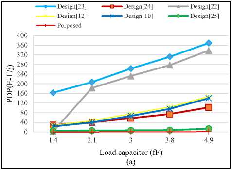
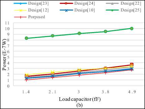
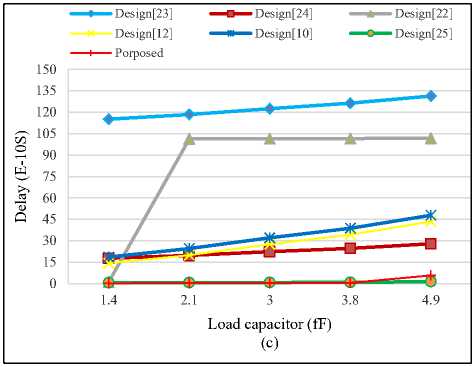
Fig.9. (a) PDP, (b) power consumption, Delay (c) vs. load capacitance.
Results can be examined in Fig.9, where the proposed compressor circuit shows off even if a large load capacitance is used. Delay, power consumption, and PDP are plotted in Fig.9 in order to achieve lowest delay, power consumption, and PDP.
-
D. Operating Frequency Analysis
In this analysis, compressor circuits are simulated in various frequencies ranges of 250, 400, and 500MH with 0.65V power supply, temperature of 27°C, and 2.1fF load capacitor.
Table 3. Simulation results in 27○C with 0.65V and c-load 2.1fF in different frequencies.
|
Frequency (MHz) |
250MH |
400MH |
500MH |
|
Delay (×10-10s) |
|||
|
CNT-Design [23] |
40.384 |
25.384 |
20.387 |
|
CNT-Design [24] |
0.42434 |
0.42551 |
0.66334 |
|
CNT-Design [22] |
40.314 |
25.315 |
20.314 |
|
CNT-Design [12] |
40.332 |
25.339 |
20.344 |
|
CNT-Design [10] |
0.42466 |
0.42489 |
0.42688 |
|
CNT-Design [25] |
0.72815 |
0.72501 |
0.73107 |
|
CNT-Proposed Design |
0.27641 |
0.2767 |
0.28002 |
|
Average Power (×10-7w) |
|||
|
CNT-Design [23] |
161.84 |
164.14 |
165.63 |
|
CNT-Design [24] |
4.1033 |
6.6269 |
4.7265 |
|
CNT-Design [22] |
3.8414 |
6.1898 |
7.6943 |
|
CNT-Design [12] |
4.3429 |
6.9578 |
8.6932 |
|
CNT-Design [10] |
3.4901 |
5.4331 |
6.7791 |
|
CNT-Design [25] |
10.757 |
12.825 |
14.22 |
|
CNT-Proposed Design |
3.2581 |
5.1385 |
6.3813 |
|
Leakage PDP (×10-17j) |
|||
|
CNT-Design [23] |
6535.6 |
4166.5 |
3376.7 |
|
CNT-Design [24] |
1.7412 |
2.8198 |
3.1353 |
|
CNT-Design [22] |
154.86 |
156.69 |
156.30 |
|
CNT-Design [12] |
175.16 |
176.31 |
176.85 |
|
CNT-Design [10] |
1.4821 |
2.3085 |
2.8938 |
|
CNT-Design [25] |
7.8330 |
9.2984 |
10.395 |
|
CNT-Proposed Design |
0.90056 |
1.4218 |
1.7869 |
Simulation results for delay, power and PDP are shown in Table 3, respectively. In Table 3, it is seen that the proposed design has the best response at all frequencies. Simulation results show that the proposed 4-to-2 compressor is consistently faster and more efficient than reference designs.
-
VI. Conclusion
A new energy-efficient, high-speed and low-PDP CNFET-based 4-to-2 compressor has been proposed in this paper. Feature size scaling is a technique to improve the performance of circuits, but it leads to a variety of critical challenges when it reduces further into nano ranges. Therefore, new technologies for circuit design, including SET, QCA, and CNFET are considered among which CNFET is the more promising successor.
The proposed 4-to-2 compressor design has been evaluated in terms of delay, power supply, PDP with different frequencies and has been compared with several state-of-the-art compressor cells. Moreover, some additional experiments have been performed to evaluate the immunity of proposed design to the accuracy of fabrication and process variations. All designs of 4-to-2 compressor cells are simulated in various supply voltages, frequencies, temperatures and load capacitors using HSPICE circuit simulator. Simulation of all implemented designs has been performed by HSPICE simulation tool. 32nm-CMOS technologies have been used for simulating CMOS circuits, and 32nm-CNFET technologies have been used for simulating CNFET circuits. More importantly, all projects MOSFET once with CMOS technology and once with CNFET simulation technology, and in both cases proposed design is superior. Simulation results have demonstrated superiority of the proposed design in terms of the mentioned metrics compared to other designs.
References A New High-Performance Bridge Structure for 4-to-2 Compressor using CMOS and CNFET Technology
- J. K. Sahani and S. Singh, "Design of Full Adder Circuit Using Double Gate MOSFET," in 2015 Fifth International Conference on Advanced Computing & Communication Technologies, 2015, pp. 57-60.
- M. Bagherizadeh and M. Eshghi, "Two novel low-power and high-speed dynamic carbon nanotube full-adder cells," Nanoscale research letters, vol. 6, pp. 1-7, 2011.
- S. Lin, Y.-B. Kim, and F. Lombardi, "A novel CNTFET-based ternary logic gate design," in Circuits and Systems, 2009. MWSCAS'09. 52nd IEEE International Midwest Symposium on, 2009, pp. 435-438.
- H. Gautam and P. Bindra, "Structure and a Detailed Analysis of Various Simulation Results of CNTFET: A Review," International Journal of Scientific Engineering and Technology, vol. 4, 2015.
- M. H. Moaiyeri, R. F. Mirzaee, K. Navi, and A. Momeni, "Design and analysis of a high-performance CNFET-based Full Adder," International Journal of Electronics, vol. 99, pp. 113-130, 2012.
- M. Bagherizadeh, M. H. Moaiyeri, M. Eshghi, "Digital counter cell design using carbon nanotube FETs," in Journal of Applied Research and Technology, 2017.
- L. Dadda, "Some schemes for parallel multipliers," Alta frequenza, vol. 34, pp. 349-356, 1965.
- C. S. Wallace, "A suggestion for a fast multiplier," IEEE Transactions on electronic Computers, pp. 14-17, 1964.
- C. H. Chang, J. Gu, and M. Zhang, "Ultra low-voltage low-power CMOS 4-2 and 5-2 compressors for fast arithmetic circuits," IEEE Transactions on Circuits and Systems I: Regular Papers, vol. 51, pp. 1985-1997, 2004.
- A. Pishvaie, G. Jaberipur, and A. Jahanian, "Improved CMOS (4; 2) compressor designs for parallel multipliers," Computers & Electrical Engineering, vol. 38, pp. 1703-1716, 2012.
- M. R. Reshadinezhad, N. Charmchi, and K. Navi, "Design and Implementation of a Three-operand Multiplier through Carbon Nanotube Technology," International Journal of Modern Education and Computer Science, vol. 7, p. 44, 2015.
- A. Pishvaie, G. Jaberipur, and A. Jahanian, "Redesigned CMOS (4; 2) compressor for fast binary multipliers," Electrical and Computer Engineering, Canadian Journal of, vol. 36, pp. 111-115, 2013.
- S. Veeramachaneni, K. M. Krishna, L. Avinash, S. R. Puppala, and M. Srinivas, "Novel architectures for high-speed and low-power 3-2, 4-2 and 5-2 compressors," in 20th International Conference on VLSI Design held jointly with 6th International Conference on Embedded Systems (VLSID'07), 2007, pp. 324-329.
- M. Bagherizadeh and M. Eshghi, "New CNFET-Based Full Adder cells for Low-Power and Low-Voltage Applications," Journal of Advances in Computer Research, 2016.
- R. Zarhoun, M. H. Moaiyeri, S. S. Farahani, and K. Navi, "An efficient 5-input exclusive-OR circuit based on carbon nanotube FETs," ETRI Journal, vol. 36, pp. 89-98, 2014.
- P. L. McEuen, M. S. Fuhrer, and H. Park, "Single-walled carbon nanotube electronics," IEEE transactions on nanotechnology, vol. 1, pp. 78-85, 2002.
- S. Tabrizchi, H. Sharifi, F. Sharifi, and K. Navi, "A Novel Design Approach for Ternary Compressor Cells based on CNTFETs," Circuits, Systems, and Signal Processing, pp. 1-13, 2015.
- J. Deng, "Device modeling and circuit performance evaluation for nanoscale devices: silicon technology beyond 45 nm node and carbon nanotube field effect transistors," Stanford University, 2007.
- Y. B. Kim, Y.-B. Kim, and F. Lombardi, "A novel design methodology to optimize the speed and power of the CNTFET circuits," in Circuits and Systems, 2009. MWSCAS'09. 52nd IEEE International Midwest Symposium on, 2009, pp. 1130-1133.
- Y. S. Mehrabani and M. Eshghi, "A symmetric, multi-threshold, high-speed and efficient-energy 1-bit full adder cell design using CNFET technology," Circuits, Systems, and Signal Processing, vol. 34, pp. 739-759, 2015.
- M. H. Moaiyeri, R. F. Mirzaee, K. Navi, and O. Hashemipour, "Efficient CNTFET-based ternary full adder cells for nanoelectronics," Nano-Micro Letters, vol. 3, pp. 43-50, 2011.
- A. Pishvaie, G. Jaberipur, and A. Jahanian, "High-performance CMOS (4: 2) compressors," International Journal of Electronics, vol. 101, pp. 1511-1525, 2014.
- R. Hussin, A. Y. M. Shakaff, N. Idris, Z. Sauli, R. C. Ismail, and A. Kamarudin, "An efficient modified Booth multiplier architecture," in Electronic Design, 2008. ICED 2008. International Conference on, 2008, pp. 1-4.
- D. Baran, M. Aktan, and V. G. Oklobdzija, "Energy efficient implementation of parallel CMOS multipliers with improved compressors," in Proceedings of the 16th ACM/IEEE international symposium on Low power electronics and design, 2010, pp. 147-152.
- M. Bagherizadeh and M. Eshghi, "A New High Speed Carbon Nanotube Field Effect Transistor-Based Structure for 4-to-2 Compressor Cell," Journal of Computational and Theoretical Nanoscience, vol. 13, pp. 1006-1012, 2016.
- I. Petrousov and M. Dasygenis, "Generating custom bitwidth 4: 2 compressors in hardware description language from an online tool."
- E. Alkaldy, K. Navi, F. Sharifi, and M. H. Moaiyeri, "An ultra high-speed (4; 2) compressor with a new design approach for nanotechnology based on the multi-input majority function," Journal of Computational and Theoretical Nanoscience, vol. 11, pp. 1691-1696, 2014.
- A. Momeni, J. Han, P. Montuschi, and F. Lombardi, "Design and analysis of approximate compressors for multiplication," IEEE Transactions on Computers, vol. 64, pp. 984-994, 2015.
- K. Navi, O. Kavehei, M. Rouholamini, A. Sahafi, S. Mehrabi, and N. Dadkhahi, "Low-power and high-performance 1-bit CMOS full-adder cell," Journal of computers, vol. 3, pp. 48-54, 2008.
- O. Kavehei, M. R. Azghadi, K. Navi, and A.-P. Mirbaha, "Design of robust and high-performance 1-bit CMOS Full Adder for nanometer design," in 2008 IEEE Computer Society Annual Symposium on VLSI, 2008, pp. 10-15.
- K. Navi, H. H. Sajedi, R. F. Mirzaee, M. H. Moaiyeri, A. Jalali, and O. Kavehei, "High-speed full adder based on minority function and bridge style for nanoscale," Integration, the VLSI journal, vol. 44, pp. 155-162, 2011.
- J. Deng and H.-S. P. Wong, "A compact SPICE model for carbon-nanotube field-effect transistors including nonidealities and its application—Part I: Model of the intrinsic channel region," IEEE Transactions on Electron Devices, vol. 54, pp. 3186-3194, 2007.
