A Noise and Mismatches of Delay Cells and Their Effects on DLLs

Author: Mohammad Gholami, Gholamreza Ardeshir, Hossein Miar-Naimi
Journal: International Journal of Intelligent Systems and Applications(IJISA) @ijisa
Article in issue: 5 vol.6, 2014.
Free access
Jitter is one of the most important parameters in design of delay locked loop (DLL) based frequency synthesizer. In this paper noise and mismatches of conventional delay cells which are mainly used in the DLLs architecture are introduced completely. First, time domain equations related to noise and mismatches of conventional delay cells are reported. Then, these equations are used to calculate jitter of DLL due to mismatch and noise of delay cells. At last closed form equations are obtained which can be used in the designing of low jitter DLLs. To validate these equations, a conventional DLL is designed in TSMC 0.18um CMOS Technology.
Mismatches, Noise, Phase Errors, Jitter, DLL, Delay Locked Loo
Short address: https://sciup.org/15010555
IDR: 15010555
Text of the scientific article A Noise and Mismatches of Delay Cells and Their Effects on DLLs
Published Online April 2014 in MECS
Table 1: Comparison of PLLs and DLLs
|
DLLs |
PLLs |
|
First order system and stable |
Higher order systems and can be unstable |
|
Fast locking time |
Slow locking time |
|
Easier to design |
Hard to design |
|
Occupy smaller area |
Occupy large area |
|
No jitter accumulation |
Jitter accumulation |
|
Small jitter and phase noise |
More jitter and phase noise |
|
Usually consume lower power |
Usually consume more power |
|
More dependence to reference clock |
Lower dependence to reference clock |
|
Cannot generate fractional multiples of reference clock |
Can generate fractional multiples of reference clock |
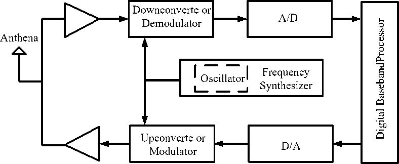
Fig. 1 shows the generic RF transceivers architecture [6]. In this figure up-conversion and down-conversion are driven by an oscillator [7, 8] which is controlled by frequency synthesizer. DLLs and PLLs are used as a frequency synthesizer in transceivers. Jitter, power consumption and phase noise are important parameters and when there is no need to generate fractional multiple of reference frequency, DLL is used instead of PLL because of its better performance. In addition, DLLs are widely used in digital communication circuits [9, 10, 11].
LNA
PA
Fig. 1: Generic RF transceiver architecture [6]
In design of frequency multiplier and clock and data recovery circuits, jitter is one of the most important parameters. In [12] analyses and experimental results on the jitter transfer of DLLs are reported. In this work z-domain model of DLL is used to obtain jitter transfer function of whole DLL. In [13] an all-digital is designed to reduce the whole jitter. To achieve this goal a duty cycle correction circuit is used. In [14] design techniques of a multiphase clock generator using a low-jitter delay-locked loop or its array for the developments of high-resolution multi-channel time-to-digital converters is presented. The low-jitter technologies for both a single DLL and an array of DLL are also discussed in [14].
Hence, designing a DLL with lower RMS jitter is of high importance. DLL has four main blocks including Chare Pump (CP), Phase Frequency Detector (PFD), Voltage Controlled Delay Line (VCDL) and Loop Filter. Non-ideal blocks and also mismatches in them result in jitter in the output of DLLs. Hence, developing an equation for describing the jitter performance of DLLs is importance. In this paper, after describing noise and mismatch of delay cells, their impacts on DLL's jitter will be analyzed.
In the next section, the conventional DLL-based frequency synthesizer will be explained. Section III describes the jitter due to noisy delay cells. Simulations and results will be presented in section IV.
-
II. Conventional Delay Locked Loop Based Multipliers
Fig 2 shows the architecture of conventional DLL. As shown in this figure, a conventional DLL consists of a Phase-Frequency Detector (PFD), a Charge Pump (CP), a Loop Filter (LF) and a Voltage Controlled Delay Line (VCDL). In a DLL, phase difference between REF and OUT signals is detected in PFD. The resulted signal at the output of PFD is sent to CP. CP and LF (integrator) generate appropriate value for control voltage of VCDL
(Vcntl) based on phase difference of REF and OUT and accordingly the delay of each delay cell is adjusted. This process is repeated until DLL is locked. It should be mentioned that in lock condition, the input and output of VCDL are in phase and the delay which is produced by VCDL is exactly equal to TREF (TREF is the period of reference clock).This means, in lock condition REF and OUT have exactly one clock period difference.
Multiplied Output
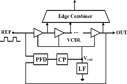
Fig. 2: Conventional DLL-based clock multiplier
An edge combiner is used when multiplied output is needed. In general edge combiner is consist of XOR gates which combine the edges at the outputs of delay cells. Fig. 3 shows the DLLs outputs with five delay stages in the delay chain. As can be seen in this figure five times of reference clock can be generated in this case. In general by N delay cells in the VCDL, N times of reference clock can be obtained when N is odd and N/2 times of reference clock can be generated when N is even. In the next section conventional delay cell is introduced and then the noise and mismatches of it will be formulized. At last the effects of noise and mismatches of delay cells will be investigated in DLLs.
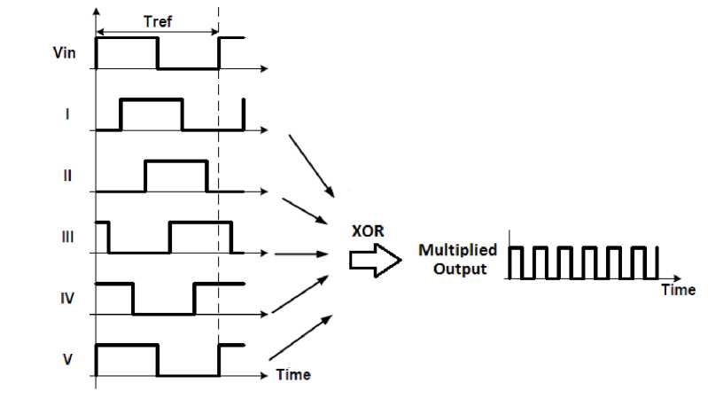
Fig. 3: Waveforms of DLL with five delay cells in the VCDL
III. Noise and Mismatch of Delay Cells and Their Effects on the DLLs
Jitter in delay cells is caused by noise and mismatching. Here, we analyse jitter produced by noise and mismatching in a conventional delay cell as done in [15].
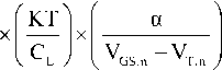
equivalent resistance of pMOS load. According to [16], the jitter of delay cells due to noise is:
° (A tDS ) TDS
KT x ---x
C L
α
V -V
GS,n T,
2.1 Jitter Due to Noisy Delay Cells
The delay of a conventional delay cell shown in Fig.4 can be written as:
Where K is Boltezman constant, T is temperature in Kelvin. α is constant parameter based on technology. Also, V is the threshould voltage of nMOS transistor.
Calculating variance of both sides of (2):
° (A tDS ) TDS
V DD
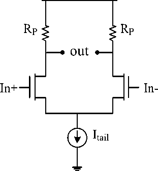
Fig. 4: Conventional Delay cells which is used in DLLs
Hence, by replacing rDS from (1) into (3):
V Y
V SW x C x ln2
L ss у
Г KT 1 f ■
\ L 7 Y
α
GS,n
—
VT
T,n у
and by simplifying this equation, a2 ( AtDs) can be written as:
°2 ( A tDS ) =
( KT ) x CL x ( Vsw x ln2 x a ) 2
Iss2 x (Vrs - V 2
SS GS,n T,n
V tds = W— x CL x In 2 = Rp x CL x ln 2
I SS (1)
In this equation T DS is the delay of each delay cell, V SW is the output voltage swing, I SS is the tail current of the delay cell, C L is the load capacitor and R P is the
For DLL with N delay stages, the jitter at the output of X-th delay stage can be obtained from:
σ2
( A t X ) « N x
( KT ) x CL x ( Vsw x ln2 x a ) 2
Iss2 x fVrs - V 2
SS GS,n T,n
2.2 Jitter of Delay Cells Due to Delay Cells Mismatch
To find the jitter produced by mismatching in delay cells, we assume that the delay of each delay cell is equal to:
Atx

X
- XTDS
DS error, j j = 1

TDS TDS + TDS
DS i DS nom DS error,i
after simplifying, Atx can be written as:
τDS where DSi is the delay of i-th delay cell, τ is the DSnom nominal delay of each delay cell and τ is the delay
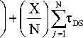
DSerror,i error of i-th cell. In lock condition of DLL, the phase difference of input and output of DLL (input and output of VCDL) exactly equal to one period of reference clock. Therefore, Eq. (8) can be written in lock condition for delay of VCDL with N delay stages as:
NX
A tx =1 n ,.^ TD' ^ TD'
V N V j = 1 j = 1
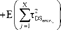
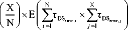
By calculating the expected value of (15) after squaring, we reach to:
2 N
E (At 2 ) = l — lx E I У4 I
X DS error,i
V N V V i =1 V т + т + + т = Т
T DS 1 + T DS 1 + ,,,+ t dS n ±REF
By applying (7) to (8):
τ DS nom
+ TDS
DS error,1
+ Tds + TDS
DS nom DS error,2
+ + T + T = T
+ ^ + TDS nom + TDS error,N T REF
The last portion of (16) can be abbreviated as:
This results in:
T
REF
τ DSnom
N
- VT
DSerror,i i =1


N
+ ^ TD'e i = X +1
N


X Z TDS er„r,j
and by substituting (10) into (7) we have:
= — X E ( T D S error )
τ DS
T
REF
N
- V
DSerror,i i =1
and by replacing it into (16):
N
DSerror,i
E ( A t — )
In lock condition when there is not jitter, the delay of
T each cell is equal to REF , and the systematic jitter of X-N th delay stage can be written as:

)

X E ( T DS errr )
X
A tX = ^T№ j =1
X X TREF N
Or equivalently:
By replacing τ from (11):
X
A t — = £ j = 1
N
TrEF - X T D' e-r r
-----—-----+ TDS
DS error,j

^ 2 ( A tX ) =

X ^ 2 ( ^ D' error )
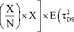
Equation (19) shows that when X=0 or X=N, the jitter due to mismatching of delay cells in output of X-th delay cells is equal to zero. Also, this equation shows that the maximum jitter in VCDL due to mismatching of delay cells happens in X=N/2. These results can be summarized as:
By expanding this equation:
min ( ° 2 ( A t X ) )
X = о ^ о2 ( A tx ) = 0
X = N ^ о2 ( A t x ) = 0
max ( °2 (A t x ) ) ^ X = N ^ °2 (A t x ) = 3 N x °2 ( г ;s )
-
IV. Simulation and Results
A conventional DLL-based frequency multiplier has been designed in TSMC 0.18µm CMOS Technology by ADS simulator to evaluate equations obtained in section III.
It should be mentioned that all building blocks have been designed by CML logic and in differential fashion to have a higher speed DLL. All building blocks of the proposed DLL have been reported in [16].
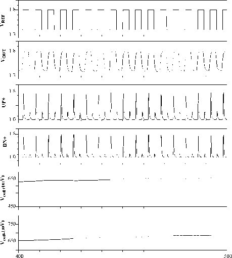
Circuit implementation of delay cell is shown Fig. 4. In addition PFD and CP which are used in this design are shown in Fig.5 and Fig.6 respectively. This DLL has been designed to evaluate the above analysis. DLL's waveforms around the lock condition are shown in Fig.7. To prove the validation of (19) and (20), simulation has been done for N=8, 12, 16, 20 in DLLs (N is number of delay stages in VCDL). The related waveforms have been shown in Fig.8. Both simulation and theoretical predictions show that jitter of DLL due to mismatch of delay cells is maximum at middle of VCDL (X=N/2) and minimum at start and end of VCDL (X=0 and X=N).
V DD
V Bias
UP-
V CMF
DN-
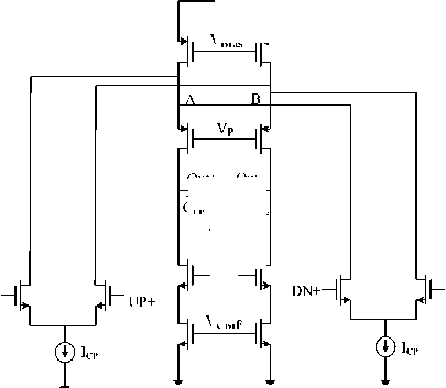
Fig. 6: Charge pump circuit for designing DLL
Out+ Out-
C LF CLF
V N
time, nsec
Fig. 7: Waveforms of DLL near lock condition
V DD
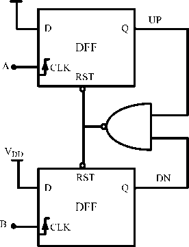
Fig. 5: Conventional PFD which is used in the design of DLL
-
V. Conclusions
In this paper noise and mismatches of conventional delay cells have been examined. First, time domain equations of related to noise and mismatches of conventional delay cells have been expressed. Then, these equations were used to calculate jitter of DLL due to mismatch and noise of delay cells. To evaluate these equations a conventional DLL has been designed in TSMC 0.18um CMOS Technology. Simulation results prove the accuracy of theoretical predictions.
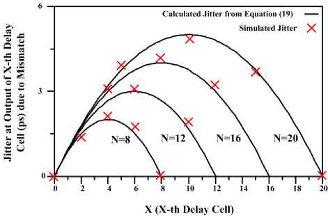
Fig. 8: Jitter at output of X-th delay cell due to mismatch versus X for different N
Acknowledgments
The authors would like to thank the anonymous reviewers for their careful reading of this paper and for their helpful comments. This work was supported in part by the Micro-Electronic Groups, Faculty of Electrical Engineering of Babol Noshirvani University of Technology.
References A Noise and Mismatches of Delay Cells and Their Effects on DLLs
- M. Gholami, Gh. Ardeshir and H. Ghonoodi, “A novel architecture for low voltage-low power DLL-based frequency multipliers”, IEICE Electron. Express, Vol. 8, No. 11, pp.859-865, (2011).
- Won-Joo Yun; Hyun-Woo Lee; Dongsuk Shin; Suki Kim; , "A 3.57 Gb/s/pin Low Jitter All-Digital DLL With Dual DCC Circuit for GDDR3 DRAM in 54-nm CMOS Technology," Very Large Scale Integration (VLSI) Systems, IEEE Transactions on , vol.19, no.9, pp.1718-1722, Sept. 2011.
- J. Lee, K. S. Kundert, and B. Razavi, “Analysis and modeling of bangbang clock and data recovery circuits,” IEEE J. Solid-State Circuits, vol. 39, pp. 1571–1580, Sep. 2004.
- Oh, K.-I.; Kim, L.-S.; Park, K.-I.; Jun, Y.-H.; Kim, K.; , "Low-jitter multi-phase digital DLL with closest edge selection scheme for DDR memory interface," Electronics Letters , vol.44, no.19, pp.1121-1123, September 11 2008.
- C. Kim, I.-C. Hwang, and S.-M. Kang, “A low-power small-area 7.28-ps-jitter 1-GHz DLL-based clock generator,” IEEE J. Solid-State Circuits, vol. 37, pp. 1414–1420, Dec. 2002.
- Razavi B., "RF Microelectronics", Second Edition, PRENTICE HALL, 2012.
- Gholami, M.; Fallah, M., "Increasing frequency of ring oscillators by using negative capacitors," Electronics Letters , vol.48, no.18, pp.1109,1110, August 30 2012. DOI: 10.1049/el.2012.2261.
- Gholami, Mohammad and Rahimpour, Hamid., "Design and analysis of negative capacitor by using MOSFETs," International Journal of Electronics, pp.1,11, 2013. DOI: 10.1080/00207217.2013. 817023.
- Rahimpour, Hamid, Mohammad Gholami, Hossein Miar-Naimi, and Gholamreza Ardeshir. "All digital fast lock DLL-based frequency multiplier." Analog Integrated Circuits and Signal Processing (2013): 1-8. DOI: 10.1007/s10470-013-0205-9.
- Gholami, Mohammad, Hamid Rahimpour, Gholamreza Ardeshir, and Hossein Miar‐Naimi. "A new fast‐lock, low‐jitter, and all‐digital frequency synthesizer for DVB‐T receivers." International Journal of Circuit Theory and Applications (2013). DOI: 10.1002/cta.1958
- Gholami, Mohammad, Hamid Rahimpour, Gholamreza Ardeshir, and Hossein MiarNaimi. "Digital delay locked loop-based frequency synthesiser for Digital Video Broadcasting-Terrestrial receivers." Institution of Engineering and Technology (2013). DOI: 10.1049/iet-cds.2013.0169
- Lee, M.-J.E.; Dally, W.J.; Greer, T.; Hiok-Tiaq Ng; Farjad-rad, R.; Poulton, J.; Senthinathan, R., "Jitter transfer characteristics of delay-locked loops - theories and design techniques," Solid-State Circuits, IEEE Journal of , vol.38, no.4, pp.614,621, Apr 2003.
- Won-Joo Yun; Hyun-Woo Lee; Shin, Dongsuk; Suki Kim, "A 3.57 Gb/s/pin Low Jitter All-Digital DLL With Dual DCC Circuit for GDDR3 DRAM in 54-nm CMOS Technology," Very Large Scale Integration (VLSI) Systems, IEEE Transactions on , vol.19, no.9, pp.1718,1722, Sept. 2011.
- Wu Gao; Deyuan Gao; Brasse, D.; Hu-Guo, C.; Yann Hu, "Precise Multiphase Clock Generation Using Low-Jitter Delay-Locked Loop Techniques for Positron Emission Tomography Imaging," Nuclear Science, IEEE Transactions on , vol.57, no.3, pp.1063,1070, June 2010
- Weigandt, T.C.; Beomsup Kim; Gray, P.R.; , "Analysis of timing jitter in CMOS ring oscillators," Circuits and Systems, 1994. ISCAS '94., 1994 IEEE International Symposium on , vol.4, no., pp.27-30 vol.4, 30 May-2 Jun 1994.
- Gholami M.; "A Novel Low Power Architecture for DLL-Based Frequency Synthesizers," Circuits, Systems, and Signal Processing: Volume 32, Issue 2 (2013), Page 781-801. DOI: 10.1007/s00034-012-9488-9.
