A Novel Architecture for Adaptive Traffic Control in Network on Chip using Code Division Multiple Access Technique

Author: Fatemeh. Dehghani, Shahram. Darooei
Journal: International Journal of Computer Network and Information Security(IJCNIS) @ijcnis
Article in issue: 8 vol.8, 2016.
Free access
Network on chip has emerged as a long-term and effective method in Multiprocessor System-on-Chip communications in order to overcome the bottleneck in bus based communication architectures. Efficiency and performance of network on chip is so dependent on the architecture and structure of the network. In this paper a new structure and architecture for adaptive traffic control in network on chip using Code Division Multiple Access technique is presented. To solve the problem of synchronous access to bus based interconnection the code division multiple access technique was applied. In the presented structure that is based upon mesh topology and simple routing method we attempted to increase the exchanged data bandwidth rate among different cores. Also an attempt has been made to increase the performance by isolating the target address transfer path from data transfer path. The main goal of this paper is presenting a new structure to improve energy consumption, area and maximum frequency in network on chip systems using information coding and decoding techniques. The presented structure is simulated using Xilinx ISE software and the results show effectiveness of this architecture.
Code Division Multiple Access technique, Network on Chip, Adaptive traffic controls, routing
Short address: https://sciup.org/15011559
IDR: 15011559
Text of the scientific article A Novel Architecture for Adaptive Traffic Control in Network on Chip using Code Division Multiple Access Technique
Published Online August 2016 in MECS DOI: 10.5815/ijcnis.2016.08.03
Growth and development of semiconductors technology, chips complexity and also the possibility to locate millions of transistors in one single chip, has let the designers to gather tens or hundreds of process cores with high storage in a single chip. Today system on chip has evolved in sense of performance, reliability and integration capacity. The last benefit of this improvement is the growth in number of Intellectual Properties (IP) cores in a chip. The number of process cores in a chip is growing quickly considering the needs of customers and this has led to some problems [1] [2]; unfortunately the increase in number of IPs has resulted that the connections inside a chip and its elements create new problems. Considering the vital role of communications on design and performance of multi core system-on-chips and the fact that their architecture has limited wired connections and distributed computation, Network on Chips(NOC) have been introduced to optimize the system on chip design and solve their problems [3]. NOC is an emerging technology for interconnecting multiple cores on a single silicon chip [4]. The architecture of network on chip regularly consists of router, network adaptor, network interfaces and its connections [12]. Multi core processors and special Image processors are some examples of network on chips’ applications. Network on chips also suffer from challenges such as power consumption, area and delay limitation in their connections [5]. To solve the challenges of network on chip, different architectures and structures have been proposed up to now that data transfer problem in an environment with different clock domains is a considerable matter in network on chip. In addition, considering the increase in number of IP blocks in system on chip, these blocks should be able to transfer their data in different ranges of clock frequencies. However, the data transfer among the various clock domains has changed to a problem on its own. The reason is that the clocks need to be coordinated and managed in the network. To solve this problem Globally-Asynchronous Locally-Synchronous (GALS) transfer method was applied [13]. Now to get rid of delay and complexity of data transfer, different data were separated from different users in the code domain. So different users can used communication channels in parallel during the time. In this paper we attempted to decrease the size of network hardware on chip by separating the data transfer communication buses from those of code transfer’s so that the parameters like area, maximum frequency and delay can be enhanced. The rest of this paper is arranged as follows. In section II of this paper the structure of code division multiple access algorithms will be discussed. We introduce our proposed architecture in Section III, IV. The simulation results have been presented in section V, VI before concluding in Section VII.
-
II. Code Division Multiple Acceess Algorithm
Code division multiple access technique (CDMA) has been proposed as a new connection mechanism for generations of embedded systems (ESs) recently. Compared to a conventional Time division multiple access (TDMA) based bus, a CDMA based bus has better features concerning channel's isolation and channel's continuity in time domain since channels are divided by the spreading codes [11]. CDMA technology works based on code-word orthogonality.
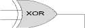
Several code-words gather together at any point of time so they don’t interfere and can separate from each other without losing information [6] [10]. Orthogonality code-words are used for users to encode their data before transmitting them to shared communication channels. Hence, different users can use shared communication channels simultaneously by encoding their own data [2]. Information encoding in analog circuits are achieved using constant voltage and capacitance. So, data transmission onto analog buses may encounter problems such as coupling noise, clock skew and changes in capacitor and resistor due to circuit implementation [7]. To avoid the challenges available in analog circuits, CDMA-based encoding and decoding digital designs have been developed in network on chips. Coding digital design is illustrated in figure 1 [2].
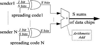
Fig.1. Encoding CDMA [8]
The decoding design consists of two separate positive and negative parts and use spreading codes for data decoding. For example as illustrated in figure 2, if the first bit of spreading code is zero, the first bit resulted from S sum will enter positive accumulator, otherwise the data will get into the negative accumulator. Selecting the data and storing them in accumulators will be done similarly on other values in S sum. After data storing operation in the accumulators, if the value of the positive accumulator is larger than the value in the negative accumulator, the original data bit is “1”; otherwise, the original data bit is “0” [2].
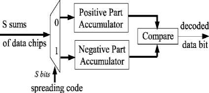
Fig.2. Decoding CDMA [8]
-
III. Proposed Architecture for Adaptive Traffic Control
Runtime traffic than the deterministic traffic Have a higher degree of adaptive and with the increased volume of traffic require a monitoring unit that the ability to dynamically be correct paths . This monitoring unit can choose better routs comparing to non-adaptive algorithms depending on traffic status. Monitoring techniques usually need large tables, while implementing such units should be done with simpler methods in network on chip. To analyze the cons and pros for 2 designs of network on chips- one design is based on CDMA technique and the other is the design proposed by this paper- network structure, data transfer principal, network nodes and their functionality will be compared. According to what was mentioned before a new structure and architecture will be introduced that is able to adaptively control traffic using information coding and decoding. To compare this architecture with other network on chip architectures, we will call it “architecture for adaptive traffic control based on CDMA”. To solve the problem of simultaneous access to the bus the code division multiple access technique has been used. This algorithm has been proposed by applying CDMA technique- this technique was explained in section A- and by eliminating monitoring in runtime’s adaptive algorithm. The proposed architecture will be explained in details in the next section.
-
IV. Adaptive Traffic Control Architecture with Information Coding and Decoding
Proposed structure and architecture consists of nodes, router and communication bus that each of which will be explained in the following sections.
Node : Each multi-processor system on chip and network on chip architecture contains several information processing nodes. Comparing to single-core processors, the final purpose of increasing processor nodes is raising computation capacity and efficient and affordable energy. Each node consists of a simple-designed router, a processing unit, a shift register and an encoder. These 4 elements together form an information node. The router design and node structure are demonstrated in figure 3. So that considered for each node a register with 5 slots.
As it is shown is figure 3, these 5 input and outputs are used for communicating with other nodes. In addition, in this structure CDMA transmit unit is used for coding purposes (this will be explained in the next section). Shift register unit is used for saving switches status and so this unit is helpful to control the switches status for information exchange.
Router: Router in this architecture has 5 inputs and outputs that their status can be in on or off modes. Off status shows situation when data are not exchanged and on status is considered when data exchange occurs. After information coding and decoding, switches in each node should be set in on or off status. In fact switches determine the route path for information packets submitted by processors. Designing a router for chip’s interconnections depends on parameters like area, speed and power. An attempt using a simple and efficient mechanism was made in this design to decrease hardware area in network on chip and enhance router performance. The design of this router is scalable. It means that choosing longer Walsh code and increasing IP cores connected to the router is possible for it. The purpose of designing suitable communication link is minimizing the network costs in terms of area, power and simultaneously preserving service quality in regard to acceptable delay for information packets. To increase the performance of nodes interconnections and data flow control in network two kinds of bus will be used.
— -► Request link
-*---► Data link
► Configuration link
---► Code bus
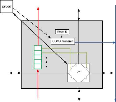
Fig.3. The Node and Router Structure in Proposed Network on Chip Architecture
Data bus: These buses are used for exchanging processing information. In other words, after the route is determined data transfere will be done using these buses.
Code bus:Code buses are used for exchanging coded information. This bus is considered as a one-bit bus. These buses are designed in a 2-way format. It means when leaving the encoded information will be located on the bus and while coming back decoded information will be located on the bus. In each clock pulse one bit of information will be transferred to the bus. This is the common clock pulse for all the resources. More details about this structure can be seen in figure 4. Black lines are used for data exchange, gray and blue lines are used for code exchange. Blue lines are considered for transferring coded information and gray lines are dedicated for transferring decoded information. Since just one node can access the bus in each period of time, data coding method will be used so that all the 3 nodes can put their data on the bus simultaneously. Implementation of proposed architecture is done based upon mesh 3*3 topology. For this mesh topolgy with 3*3 dimensions, 3 one-bit buses should be considered in a way that each 3 nodes have one common bus. Each one of these buses are designed as an one-bit bus that will enter decoding unit. In this unit the input data should be decoded first so that the packets destination addresses can be extracted. Then using a specified algorithm that can be an optimized routing algorithm in network on chip packet routing will be done. The software algorithm unit in this paper is considered as a routing table in which each node destination address (each node that contains information) in addition to its source destination is written. Different phases for this algorithm will be explained in the next section.
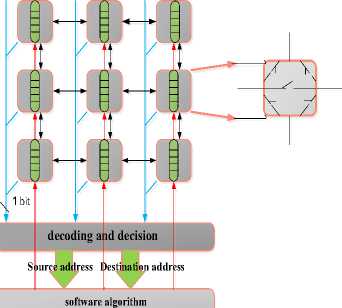
Fig.4. Structure of the used Node and Router in the Proposed Structure
Procedure of the algorithm is as follows:
First phase : To transfer data packets from source node to destination node, at first the destination address should be extracted from submitted packet information. In the previous architectures processing data and destination information both were submitted through data bus. In other words there were no isolated buses available for transferring processing data and the information available in packets. This could result in an increase in network traffic and could even cause bottleneck in case of high rate of network congestion. Different suggestions have been presented up to now to solve this problem. However, in order to gain higher performance in the proposed algorithm of this paper the data transfer buses have been separated from those of destination addresses. In this algorithm a unique 4-bit Walsh code is dedicated to each node in mesh topology. This code is preserved for each node specifically. Submitted data packet which contains destination address will be coded based on Walsh code for that node. The coding process can be seen in figure 5 schematically.
All 3 users will XOR information related to submitted packet‘s destination address with the node’s related Walsh code.

Walsh1 code
User 2
Walsh 2 code


User 3
Walsh 3 code
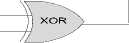
Fig.5. Information Coding with 3 User
Then the coded information by 3 users will be sent serially at the time unit. All nodes that are located in a row are synchronous with each other by a signal called syncIn, and if the signal ComReq is equal to one, code operations is going to begin. So that 32 clock pulses should pass for a 4-bit destination address to takes place en coding operation. In other words, whenever data is available to encode and ComReq is equal to one, SyncIn must one to be ready to send and code data. For every bit of the destination address , a counter as AdrIndexCnt and for every bit of Walsh code, a counter as CodIndexCnt exist, CodIndexCnt counter counts from 0 to 7 (8-bit Walsh code), and after ,the interval counter AdrIndexCnt is incremented. In other words, whenever the destination's address counter activates, Walsh code counter should pass 8 clocks, so that two counter code and destination addresses are matched with each other. When the coding operation is finished, a signal as SyncOut activates to announce the other units that coded data is going to transfer. Then, the coded data will start to move for sending. A global clock is considered for all the nodes in this structure. All nodes in a row are to be synchronized with each other by a signal called syncIn. For nodes to be synchronized, all the nodes will set their output to zero after coding. So that if a node has no data to submit other nodes in the column can continue their activity without any problem. As a result if one of the nodes in the column has a data to submit and others have no data to submit no problem will occur for other nodes because we have set the signal to zero for nodes not submitting the data.
Second phase: The submitted information on to the bus will enter decoding and decision making phase. In this phase, firstly the input data should be decoded. Data will enter serially to each of the decoders. Each input data bit will be compared to the bit of Walsh code. If the input data and the code’s Walsh bit are both 1 the input data will get into the accumulator 1 and if the code Walsh bit is zero data will get into accumulator 0. After filling the accumulators it should be analyzed that which one of the ACs consists of 4 ones. If any of the ACs has 4 ones that AC will be candidate for decoding bit. After decoding phase in last phase we will have a four bit data for each node. In this phase decoding data shows destination address. In fact the source address can also be gained from this information because Walsh code address is unique for each source. Sender counter can also be extracted considering this address. This operating unit includes a 4-bit signal called SyncIn and DataEncodport that each bit represents a column. This means that DataEncod(0) represents the first column, and so on continues until the 4th column. Walsh codes for each node are going to in the initialize testing program to be considered as a generic for decoder program. When SyncIn enters to the decoder unit, the imported data should be decoded. In this operational unit, as per units inserted in a column, 2 storages of 0 and 1 should be considered. So, for a 4 × 4 mesh, decoder 16 should be placed with two accumulators 0 and 1. If it's first SyncIn column is active, so DataEncod will be activate, this signal is going to active as 32 clocks. In these 32 clocks, every 8 to 32 Entered data should compare with Walsh code. As a result, data is entered to the storage 4 times.
In other words, when data is activated with activating SyncIn(0), 4 storage that are located in a column (numbers 00 to 03) will start their activities. If the unit is working properly that one of its storage with 0 or 1 has four 1 value. Otherwise, the node is not put data on line. As a result, a signal Disflagis activating to define as not sending code from considered node. When we get the data, at first DataEncod is transmitted to the registry called RcvBit and enables SyncOut signal every 255 clock to repeat our request to send and not send data. What has been said till now is common about all the decoders. But DecodEn signal is common for each column and between 4 nodes. So, DecodEn is activated as much as 32-bit. Also, CodIndexCnt counters that count Walsh code 8-bit and AdrIndexCnt that counters the destination address belong for each column.
In order to separate the different nodes, two joint counters should be used in the field. So, the data can be entered simultaneously into 4 decoders. Finally, we will have two outputs DesAddOut and RoutReq. As a result, this operation is repeated for each node in each column. used Switches in each node includes dual-port SwitchState, UpdateFlag and 5-port left, right, top, bottom and center, where the UpdateFlag signal are common in a column. As 20-bit data is sent to the switch after decoding, so for each of the switches, 0 to 4 belongs to the first node, 5 to 9 belongs to the second node and this trend will continues so on. For synchronizing nodes after finishing work, all nodes put their outputs on zero after coding. As the node has no data to send, the rest of the column node can continue their work without any problems.
Data will enter serially to each of the decoders
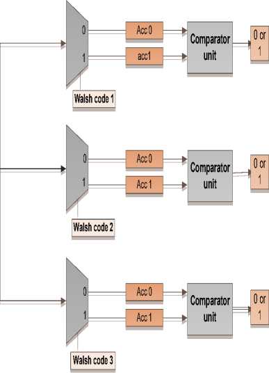
Fig.6. Information Decoding with 3 Users
As a result, if one column of data nodesis as sending data and the other nodes have no data to send, as we put no sending data as arranging signal to zero,it will be no problem with other nodes. After decoding operations at the final level, a 4-bit data will be existed for each node. At this level, decoding data is indicative as a destination address, so, the source address is derived from this information. As Walsh code's address is unique for each source, the number of sending node could be obtained according to this address. More details about this structure can be seen in figure 6.
Third phase: In this phase, the data will be sent to the software algorithm so that the transfer path gets determined using this block on data transfer lines. In fact the resource addresses and destination addresses of packages will be given to algorithm to determine their path of data. The algorithm consists of a routing table that source and destination address for each packet will be determined in that table. Then using one-bit bus lines that are considered for returning submitted data, each router’s status will get determined. As mentioned before each router consists of one register with 5 slots in which the switches on or off status will be determined. So for a 4*4 mesh topology, in each return we should submit 20 bits of data that these 20 bits will determine the status of 4 routers. Hence, in the last phase the data transfer path will be determined because the switch status for each node is specified in this phase and data can be moved onto data bus by processors. For example, assume that for 4 intended nodes, 4 Walsh codes exist in the following table and each Walsh codes want to put information on the address bus. The procedure of information Exchanging is as following. For example, assume that for 4 intended nodes, 4 Walsh codes exist in the following table and each Walsh codes want to put information on the address bus.
Table 1. Walsh Codes for a Column Dedicated to Resources
|
Source ID |
Walsh code |
|
00 |
01010101 |
|
01 |
00110011 |
|
10 |
01100110 |
|
11 |
00001111 |
The procedure of information Exchanging is as following. For example, assume that for 4 intended nodes, 4 Walsh codes exist in the following table and each Walsh codes want to put information on the address bus. The procedure of information Exchanging is as following.
Proposed architecture is designed and implemented using VHDL language. In this structure 16 nodes have been simulated and synthesized using ISE software. Additionally, the functional behavior of this architecture has been confirmed by ModelSim software. In the test level, the function behavior or designed switches and coder and decoder performance also will be studied. In order to test the behavior of switches, at first activates the switch inputs. For example, UP input is activated. When the updateflag signal is equal to one, 20 bits of information should be started to send data. This signal is common between all the switches. Each switch depending on the position must extract 5-bit information from 20-bit sending data. The position of each of them is determined to remove data by signal called row. This means that if the row is equal to zero, first 5 bits should be removed and if the first 5 bits is equal to one, the second 5 bits are extracted. As shown in the simulation, row is considered to the one. So, switches begin to remove the data in 6th clock. The number that is extracted from state of the 6th clock is equal to 00110 (when the decimal is equal to 6). This means that switch should be set on the r -> u. In this situation, right should be thrown in UP. So when a new updateflag is not inserted into nodes, this trend will continue. A new updateflag will be inserted again in the next step that its second 5 bits is considered and these 5 bits is equal 01010 that should be thrown in to d -> r. For more information about how to test, it must be said that in the test program a clock is made with a period of 20 nanoseconds. Then updateflag signal is equal to one at 50 nanoseconds a re-sets to zero and then at 70 nanoseconds. Then, it is set into one in 530 nanoseconds and is set into in and 550 nanoseconds. State is made in testing program with intervals of 20 nanoseconds. More details about this structure can be seen in figure 7.
In phase of Coding and decoding information test, at first we have been calling Encode and Decode. Bits are registered by using rcvbit once. By entering signal syncin, two address counter and code counter (adrindex, codindex) begin to operate. As shown in the waveforms, 8 clocks should be passed from code per each bit of address. Decoenable signal indicates the activation and coding. In chart, Decoenable0 means that zero columns is activated. As noted above, two storage operations are required in order to decode (accz00, accone00). According to Walsh code, any of the data are entered in one of the zero or one storages.
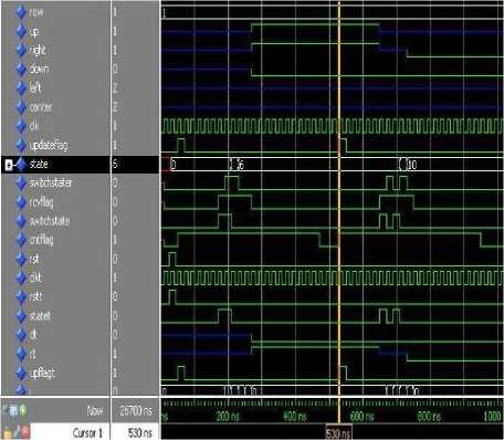
Fig.7. The Waveform of the Test Switch
When Walsh code is zero, rcvbit data is inserted into zero storage. If, for example after filling storage, 4 one values were in the storage, that storage is representative of according bit as zero or one. If zero storage has 4 one values, desired bit is equal to zero. The same operation will be repeated for all nodes. If none of storage has 4 one values, a disflag signal is activated. More details about this structure can be seen in figure 8.
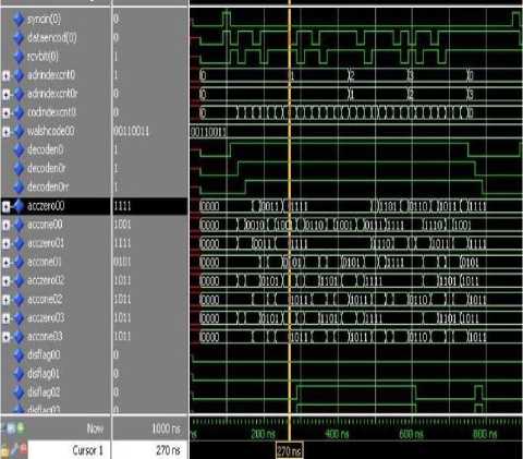
Fig.8. Waveform Related for Coding and Decoding Information to Test
In the proposed architecture the area used by different devices will be analyzed so that the best device in sense of resource consumption can be determined. The results for this structure using various devices are listed in the following table. Comparing the results while applying different devices will be helpful to distinguish best result in terms of used area, number of gates applied, delay and best frequency. At last, a classified collection of results and comparisons for different devices will be explained in table II. Fewer consumption resources and area will be occupied comparing to other FPGA families, when devices from Virtex5 family are used. So while using Virtex5, resource consumption will be enhanced about 10% comparing to when Virtex4 is used and will be enhanced about 30% comparing to when Spartan3E is applied. Hence, Virtex5 will be used as the comparison pattern for information coding and decoding. The results for information coding and decoding in our proposed architecture and the presented structure in [9] can be seen and compared in Table III.
Table 2. Comparing the Results for Different Devices Using Proposed Architecture
|
Device |
Area |
Delay |
Max frequency |
|
Spartan3E |
86% |
4.280ns |
201.086MHz |
|
Virtex4 |
65% |
2.297ns |
435.294Mhz |
|
Virtex5 |
56% |
2.005ns |
498.778MHz |
Table 3. Comparing Proposed Architecture with the Presented Structure in [9]
|
Power(mw) |
Latency(ns) |
Area |
|
|
388* |
1.656ns |
73% |
Coding in proposed architecture |
|
5.1+0.9 |
23.2ns |
81.6% |
Coding in [9] |
|
388* |
1.839ns |
45% |
Decoding in proposed architecture |
|
5.1+0.9 |
14.7ns |
35.6% |
Decoding in [9] |
* P resented power is the summation of power in coding and decoding phases .
As demonstrated in table 2, when virtex5 family members are applied proposed structure shows an enhancement in consumed area comparing to proposed structure in [9]- this enhancement is about 8.6 in coding phase and about 9.4% in decoding phase. Similarly, latency shows an enhancement about 21.55ns in coding phase and about 15.861ns in decoding phase.
-
V. Comparing the Two Proposal and Plan based on Multiple Access Techniques with Code Division
Proposal and the previous structure of the network will be compared as structure network, principles data transmission and design of network nodes and their performances.
Principle of data Transmission: in network on chip based on Multiple Access with Code Division, transmitting data packets are coded from different nodes and are moving through the channels between nodes in the realm of time and space. While in the proposal plan, encoded data move from different nodes on a code links and data in its original form on the data exchange links.
Structure nodes: node structure is simple in the proposed structure that the communication control tasks
Simulate the usual appearance of papers in a Journal of the Academy Publisher. We are requesting that you follow these guidelines as closely as possible. in the network nodes are far fewer nodes in chip based on Multiple Access with Code Division. But both projects have tried to avoid the complexity of the routing process in the network nodes.
Asynchronous design: In proposal plan, making decisions is done as Global and data transmitting is Local, which reduces the amount of hardware. While in the past design, making decisions and sending data is Global.
Estimated Performance: In the case where Virtex5 family is used, occupies compared to other FPGA families in less resource consumption and area.
-
VI. Conclusion
Considering the major problems existing in network on chip including buffer size, scalability and IP mapping problems an attempt was made to firstly explain the code division multiple access technique and its coding and decoding algorithm. Then the code division multiple access technique was implemented using digital circuits and by Xilinx ISE14.2. Applying this technique in network on chip will result in higher performance and fewer overhead in network. In addition, the main advantage of this scheme is to transmit data simultaneously on the network and development of the project in a hierarchical network, will make a network as scalable. Constant data transmission delay is useful in network based on multiple access techniques with code division to provide communication services guaranteed in a system based on chip and transmitting data will easily be possible using multiple access features. In the proposed architecture which is based on mesh topology and simple routing method an attempt was made to increase the bandwidth rate for transferring information between different cores. Then using proposed structure and by isolating data transfer buses from code transfer buses we tried to introduce a structure with simple design that is able to reduce the resource consumption and increase the performance significantly. According to aforementioned information it is noteworthy that using simple routing design in this structure will cause a scalable structure to be formed. So, one of the issues proposed to continue in this research is that, increase reliability and better use, fault-tolerant methods can be used to serve about quality of service in this structure. Also, using efficient routing algorithms according to presented structure and its features in software algorithm to find the optimal route will be able to decrease the delay between the transmitter and receiver in addition to having a constant value.
References A Novel Architecture for Adaptive Traffic Control in Network on Chip using Code Division Multiple Access Technique
- A. Shacham, K. Bergman, and L. P. Carloni, "Photonic networks-on-chip for future generations of chip multiprocessors," IEEE Transactions on Computers, vol. 57, No. 9, pp. 1246-1260, 2008.
- X. Wang, T. Ahonen, and J. Nurmi, "Applying CDMA technique to network-on-chip," Very Large Scale Integration (VLSI) Systems, IEEE Transactions on, vol .15, No. 10, pp. 1091-1100, 2007.
- L. P. Carloni, P. Pande, and Y. Xie, "Networks-on-chip in emerging interconnect paradigms: Advantages and challenges," In Proceedings of the 2009 3rd ACM/IEEE International Symposium on Networks-on-Chip, IEEE Computer Society, pp. 93-102, 2009.
- S. Venugopal, A. Arulanandasamy, and R. Ramachandran, "Efficient Router Architecture Design on FPGA for Torus based Network on Chip," International Journal of Computer Applications, vol. 55, 2012.
- M. A. Al Faruque, T. Ebi, and J. Henkel, "AdNOC: runtime adaptive network-on-chip architecture," Very Large Scale Integration (VLSI) Systems, vol. 20, No. 2, pp. 257-269, 2012.
- T. Nikolic, G. Djordjevic, and M. Stojcev, "Simultaneous data transfers over peripheral bus using CDMA technique," In Microelectronics, 26th International Conference on. IEEE, pp. 437-440, 2008.
- M. Takahash, B. Tan, H. Iwamura, T. Matsuoka, and K. Taniguchi, "A study of robustness and coupling-noise immunity on simultaneous data transfer CDMA bus interface," In Circuits and Systems, IEEE International Symposium on, vol. 4, pp. IV-611, 2002.
- X. Tian, "Implementation of Message Scheduling on TDM Virtual Circuits for Network-on-Chip," PhD diss., School for Information and Communication Technology, Royal Institute of Technology, Stockholm, Sweden, 2008.
- A. A. El Badry and M. A. A. E. Ghany, "CDMA technique for Network-on-Chip," In Design and Diagnostics of Electronic Circuits & Systems (DDECS), pp. 163-166, 2012.
- V. Ravichandran, G. K. D. PrasannaVenkatesan, R. Rani, "CDMA coding techniques for interconnect between ip cores," IOSR Journal of Engineering (IOSRJEN), vol. 2, Issue 9, PP. 84-90, 2012.
- T. Nikolic, M. Stojcev, and G. Djordjevic, "CDMA bus-based on-chip interconnect infrastructure," Microelectronics Reliability, vol. 49, no. 4, pp. 448-459, 2009.
- A. B. Achballah and S. B. Saoud, "A Survey of Network-On-Chip Tools," International Journal of Research and Reviews in Computer Science (IJRRCS), vol .2, No. 9, 2013.
- B. Nagaveni, G. Sai Thirumal, M. Rami Reddy, "Implementation of Network On-Chip Using GALS Scheme," international journal of scientific & technology research, vol. 2, issue 5, 2013.
