A Novel Circuit for Thermocouple Signals Linearization Using AD Converter

Author: Ayman A. Aly, Aly S. Abo El-Lail
Journal: International Journal of Information Technology and Computer Science(IJITCS) @ijitcs
Article in issue: 3 Vol. 5, 2013.
Free access
A novel circuit for linearization of thermocouple signals using Analog – to – Digital converter (ADC) is proposed. The present method utilizes the ratio metric property of ADCs and the converter performs analog to digital conversion as well as linearization. The resulting circuit also has provision for scaling the linearized digital output to obtain a desired full-scale value. Computational studies carried out on the proposed method gives satisfactory results for thermocouples with monotonic concave upward and downward characteristics.
Thermocouple, Linearization, Analog – to – Digital Converter, Scaling
Short address: https://sciup.org/15011838
IDR: 15011838
Text of the scientific article A Novel Circuit for Thermocouple Signals Linearization Using AD Converter
Published Online February 2013 in MECS
Most of the transducer characteristics are almost nonlinear in nature. Even for thermocouples with decent linearity the nonlinearity is not too small to ignore. It is therefore imperative that linearization techniques be also employed for thermocouple based temperature measurement systems.
Allen R. Parker, Jr. 1993, has described a new signalconditioning technique for measuring strain and temperature which uses fewer connecting wires than conventional techniques. Simultaneous measurement of temperature and strain has been achieved by using thermocouple wire to connect strain gages to signal conditioning. This signal conditioning uses a new method for demultiplexing sampled analog signals and the Anderson current loop circuit.
[Ian Galton, 2000], described an all-digital technique that significantly measures and cancels the portion of the ADC error arising from DAC noise during normal operation of the ADC, so no special calibration signal or auto-calibration phase is required. The details of the technique are described in the context of a nominal 14-bit pipelined ADC example at both the signal processing and register transfer levels.
X. Wang, P. Kiss, etl., 2001, introduced an adaptive digital algorithm for acquiring and correcting the errors of the feedback DAC used in a multibit S ADC. The method is highly accurate, and is particularly useful for wide band ADCs, where mismatch error shaping becomes ineffective.
The generalized software based linearization techniques for transducers [Ghosh and Patranabis, 1991] [Patranabis and Ghosh, 1988] can also be used for the thermocouples. However in literature, the results of application of these methods to thermoelectric transducers have seldom been reported. So far as hardware based methods are concerned, in research publications one rarely comes across linearizing circuits developed for thermocouples.
In the present work, a relatively inexpensive hardware method for linearization of thermocouple signals using ratiometric property of ADC has been proposed. The present method using ADC is an improvement on the basis method proposed earlier [Iglesias and Iglesias], in the sense that the modified scheme uses independent linearization and scaling arrangements.
The remainder of this paper is organized as follows: Section 2 gives the theory of the proposed circuit. Section 3 illustrates the circuit analysis. Section 4 presents the results and discussions. Conclusion is given in the final section.
-
II. Theory of the Proposed Circuit
The digital count output L of dual-slope integration type A/D converter with differential input is given by
L=c (VN- vm)
V
Re f (1)
where
are the analog input voltages,
Ref is an analog reference voltage, and C is the
digital count output when (
) =
V+
If IN is the voltage signal E(x) from a transducer circuit (x being measured), following an approach proposed by Iglesias et al., a quasi – linear relation between
L (x) and x can be achieved by suitably modifying the equation (1) such that,
Suppose it is desired that at the full-scale value of x f of the measured temperature, the digital output should be L(x f )=AC. Where the maximum possible value of A depends on the ADC under consideration.
As an example, for INTERSIL ICL 7135 ADC, the maximum allowable value of A is 2. Then,
E (x f ) E r = A [1+K (1–A)] (3)
The constant A represents the sensitivity of the arrangement. Over a certain span of temperature, based on a desired value of A, an optimum value of K can be obtained. Er can be adjusted to achieve the desired value of A. For the same span of temperature, if it is required to have an increased sensitivity A by changing E r , the linearity will be disturbed. Hence this method of achieving a desired full-scale digital output has not been considered.
where the analog reference voltage is for positive K,
Ref r for negative K,
K is the linearizing coefficient, whose optimum value is to be determined.
For the two cases, the expressions for the linearizing coefficient in terms of circuit resistances are K=R 2 / R 1 and K = - R 2 / (R 1 +R 2 ) respectively.
In our case, x is the temperature T under measurement and E(x) is E(T) - the thermo-emf from the thermocouple after appropriate reference junction compensation.
As an alternate approach, the linearizing arrangement is so designed that the scaling and linearizing mechanisms are independent of each other. Then the digital output count is given by,
where A is the scaling constant. If E r is adjusted to E(x f ), the full-scale digital output is L(x f ) = AC, Then,
The block diagram representations of relevant circuits are given in Fig.1 (for positive K) and Fig.2 (for negative K).
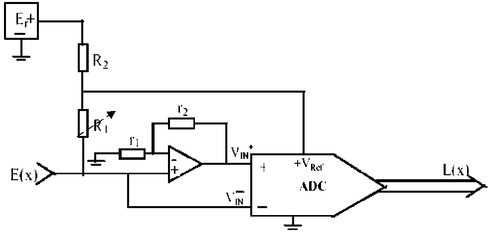
Fig. 1: Block Diagram of the Proposed Linearizing Circuit for Positive ‘K’
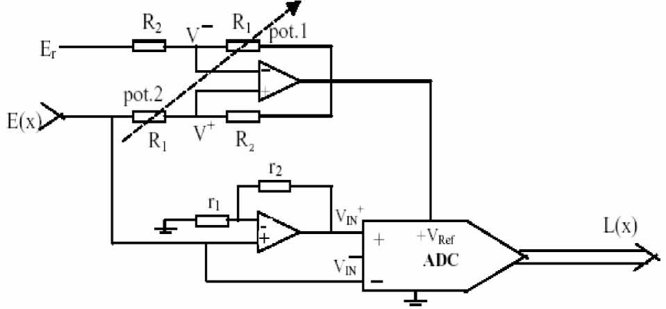
Fig. 2: Block Diagram of the Proposed Linearizing Circuit for Negative ‘K’
The normalised deviation of L (x) vs x characteristic from linearity for any value of x is,
D(K,x) = L(K,x) -—
L(K,xf) xf
The optimum value of K, is obtained by numerically minimizing D2 (K, x) as a function K. The sum-squared deviation is given by
N
S = 2 D2(K,Xn) n = 1
where N denotes the number of x values considered for computation. An approximate value of K=K* is obtained by imposing the condition,
L(xf ) = 2L(xf / 2)
The optimum value of K is then obtained by varying K in steps about the value K* and computing S for each value of K by varying x in steps from 0 to x f . Value of K for which S is minimum, is chosen as the optimum one.
The optimum value of K will attain positive sign for concave upward signals (negative nonlinearity) and negative for concave downward signals (positive nonlinearity).
VIN E(x ) = E(x)(10)
E K
VRef(x) = — +
1 + K 1 + K where, K = ( R2 / R1) is the linearizing coefficient.
The digital output of the ADC is as given in equation 4.
where, A= (r 2 / r 1 ) is the scaling constant.
For Negative K
In the circuit shown in Fig.2,
RR
V^=---2— V, (Xx) +
R + R2 Rz R + R2
V += —R— VR (X x)+RE
R + R R /V } Rx + R V 7
Since V+ should be equal to V -,
E K
VRef (x)=—— +E(x)
Re 1 + K 1 + K
III. Circuit Analysis
For Positive K
In the circuit shown in Fig.1,
where, K = (–R2/ R1) is the linearizing coefficient.
Again,
VIN = [1 + (r2/r1)]E(x)
and
VI+N=[1+(r2/r1)]E(x)
VIN = E(x)
,
The digital count output L(x) is as expressed in equation (4). It is quite obvious that pot.1 and pot.2 are ganged. It should also be ensured that R2 is always less than R1.
It is to be noted that if E(x) is zero when x is zero, for both the circuits shown in Fig.1 and Fig.2, L(0) is zero. In both cases, full-scale calibration can be carried out as follows:
-
(i) Setting the measurand x = x f , and A=1, E r is adjusted to make L(x f ) = C. This can be achieved with E r = E(x f ).
-
(ii) Then A can be adjusted to obtain the desired value of full scale ADC output L (x f ) = AC.
For both schemes, with x = x f , the reference voltage of the ADC is V Ref (x f ) = E (x f ). After the full-scale calibration is carried out, the linearizing coefficient K should be adjusted to its optimum value obtained by an appropriate method.
-
IV. Results and Discussions
In order to assess the performance of the proposed circuits, computational studies have been carried out using the manufacturer’s data for Copper-Constantan (T-type) and Iron-Constantan (J-type) thermocouples [Dhal,1962], considering different temperature ranges for each type. The specifications of a dual slope INTERSIL ICL 7135A/D converter in its standard configuration, having a full-scale voltage of 2V and
C=10000, have been considered in this study. Scaling constant (A), reference voltage (E r ) and optimum value of linearizing coefficient (K) have been determined for T-type (0 oC -300 oC and 0 oC - 400 oC) and J-type (0 oC -300 oC and 0 oC -760 oC). These values are tabulated in Table 1.
Before Lin.
After Lin.
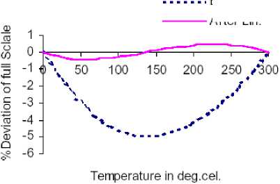
Fig. 3: Percent deviation of full scale as a function of temperature for T-type thermocouple over the range 0 to 300 oC
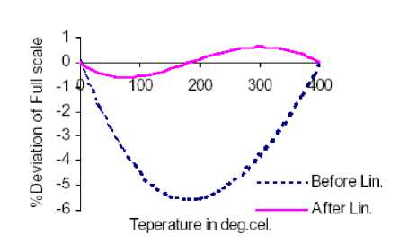
Fig. 4: Percent deviation of full scale as a function of temperature for T-type thermocouple over the range 0 to 400 oC
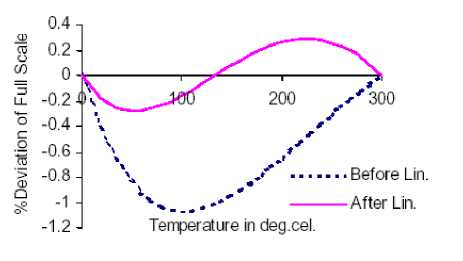
Fig. 5: Percent deviation of full scale as a function of temperature for J-type thermocouple over the range 0 to 300 oC
Table 1: Optimum value of K for T and J type thermocouple
|
Type |
Temp. Range oC |
K |
A |
Er, mV |
|
T |
0-300 |
0.222 |
0.03 |
14.860 |
|
0-400 |
0.254 |
0.04 |
20.869 |
|
|
J |
0-300 |
0.042 |
0.03 |
16.325 |
|
0-760 |
0.083 |
0.076 |
42.922 |
The plots of % deviation from linearity as a function of temperature, before and after linearization, are given in Fig.3 for T-type thermocouple over the temperature range 0 oC -300 oC. It is clearly seen from the plot that the magnitude of maximum deviation before and after linearization is 4.917% (equivalent to 14.751 oC) and 0.447% (equivalent to 1.341 oC). Likewise, in Fig.4, for the temperature range 0 oC -400 oC, after linearization, the magnitude of maximum deviation is 0.623%(equivalent to 1.869 oC) and its value is 5.540%(equivalent to 22.16 oC) before linearization.
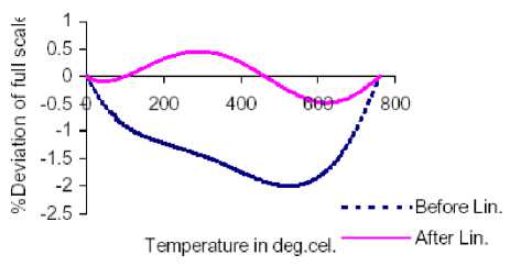
Fig. 6: Percent deviation of full scale as a function of temperature for J-type thermocouple over the range 0 to 760 oC
Fig.5 and Fig.6 depict the %deviation vs. temperature characteristics for J-type thermocouple over the temperature ranges 0 oC -300 oC and 0 oC -760 oC respectively. It is clearly observed from the plots in Fig.5 that the magnitude of maximum deviation is 1.065%(equivalent to 3.195 oC) before linearization and its value is 0.276%(equivalent to 0.828 oC) after linearization. Fig.6 portrays the way in which the %deviation of L(x) vs. x response from the linearity varies with the temperature. The observed magnitudes of maximum deviations before and after linearization are 1.998%(equivalent to 15.183 oC) and 0.447%(equivalent to 3.625 oC) respectively.
The proposed technique works extremely well for T type thermocouple. In the range 0 oC to 300 oC, the deviation from linearity is within ±0.447% which is comparable with the maximum nonlinearities of 0.36% and 0.63% obtained with Bolk’s algorithm and Lagrange interpolation respectively [Bolk,1985]. Even the value over 0 oC to 400 oC is of same order as the values obtained with the Bolk’s algorithm for a lower range of 0oC to 300 oC. For the J-type thermocouple the proposed circuit performs commendably. When used in the range 0oC to 300oC, the nonlinearity is within ±0.29%, while for the same range the maximum nonlinearity obtained by both Lagrange interpolation and Bolk’s algorithm is ±0.23% [Bolk,1985]. The results for 0 oC to 760 oC are also good, the maximum nonlinearity in this range being ±0.48% of full scale.
-
V. Conclusion
A simple hardware method to correct the thermocouple nonlinearity has been described. Numerical studies revealed that excellent results could be obtained if the proposed circuit is used for linearising signals from T and J type thermocouples. The results are comparable to those obtained by other investigators using software techniques. Thus, these thermocouples, together with appropriate inexpensive cold junction compensation arrangement and this linearising circuit can be expected to constitute a self-sufficient temperature measuring system with digital output.
-
[4] Ghosh, D. and Patranabis, D., “Linearization of Transducers Through a Generalised Software Technique”, J.Phys. E:Meas. Sci.Technol., 1991, 2,pp.102-105.
-
[5] Ian Galton, “Digital Cancellation Of D/A Converter Noise In Pipelined A/D Converters”, IEEE Transactions On Circuits And Systems—II: Analog And Digital Signal Processing, March 2000, Vol. 47, No. 3, pp 185-196.
-
[6] Iglesias, G.E and Iglesias ,E.A., “Linearization of Transducer Signals Using Analog - to – Digital Convertor”, IEEE Trans. Instrum.Meas., 1988, 37, pp.53-57.
-
[7] Patranabis, D. and Ghosh, D., “A Novel SoftwareBased Transducer Lineariser”, IEEE Trans. On Instrumentation and Measurement, 1989, 38,
pp.1122-1126.
-
[8] X. Wang, P. Kiss, U. Moon, J. Steensgaard and G. C. Temes, “Digital Estimation and Correction of DAC Errors in Multibit ΔΣ ADCs”, IEE Electronics Letters, March 2001,
Vol.37,No.7,pp.414–415,29..
Ayman A. Aly holds a BSc with excellent honour degree (top student) in 1991, MSc in Sliding Mode Control from Mechanical Engineering Department, Assiut University, Egypt in 1996 and PhD in Adaptive Fuzzy Control from Yamanashi University, Japan in 2003. He was an Assistant Professor at Assiut University from 2003–2008. Currently, he is an Associate Professor and the Head of Mechatronics Engineering Section at Taif University, Saudi Arabia. In additions to 5 text books, Ayman A. Aly is the authorand coauthor of more than 55 scientific papers in Refereed Journals and International Conferences. He supervised some of MSc. and PhD. Degree Students. His main areas of research interests are Intelligent Control of Mechatronics systems, Automotive control systems, Thermofluid systems modeling and simulation.
References A Novel Circuit for Thermocouple Signals Linearization Using AD Converter
- Allen R. Parker, Jr., “Simultaneous Measurement of Temperature and Strain Using Four Connecting Wires”, NASA Technical Memorandum 104271, National Aeronautics and Space Administration, Nov. 1993.
- Bolk, W.T., “A General Digital Linearising Method for Transducers”, J.Phys. E.Sci.Instrumn., 1985, 18, pp.61-64.
- Dahl, A.I, “Temperature, Its Measurement and Control in Science and Industry”, Reinhold Publishing Corporation, Chapman & Hall Ltd., London (1962).
- Ghosh, D. and Patranabis, D., “Linearization of Transducers Through a Generalised Software Technique”, J.Phys. E:Meas. Sci.Technol., 1991, 2,pp.102-105.
- Ian Galton, “Digital Cancellation Of D/A Converter Noise In Pipelined A/D Converters”, IEEE Transactions On Circuits And Systems—II: Analog And Digital Signal Processing, March 2000, Vol. 47, No. 3, pp 185-196.
- Iglesias, G.E and Iglesias ,E.A., “Linearization of Transducer Signals Using Analog - to – Digital Convertor”, IEEE Trans. Instrum.Meas., 1988, 37, pp.53-57.
- Patranabis, D. and Ghosh, D., “A Novel Software-Based Transducer Lineariser”, IEEE Trans. On Instrumentation and Measurement, 1989, 38, pp.1122-1126.
- X. Wang, P. Kiss, U. Moon, J. Steensgaard and G. C. Temes, “Digital Estimation and Correction of DAC Errors in Multibit Δ∑ ADCs”, IEE Electronics Letters, March 2001, Vol.37,No.7,pp.414–415,29.
