A Practical Application of ARM Cortex-M3 Processor Core in Embedded System Engineering

Author: Oluwole O. Oyetoke
Journal: International Journal of Intelligent Systems and Applications(IJISA) @ijisa
Article in issue: 7 vol.9, 2017.
Free access
Embedded Systems Engineering has grown in recent years to become an integral part of our daily living as it finds striking applications in various spheres of our lives. These range from Manufacturing, Electronic Health, Telecommunications, Construction and Robotics to numerous other fields. Primarily, Embedded Systems are usually a combination of selected electrical and electronic components functioning together under the direct control of a programmed controller. They serve fundamentally as additional units incorporated within already existing infrastructures with the sole aim of providing dedicated services to the larger infrastructure. Many of the controllers used operate on uniquely designed processor cores, instruction sets, and architecture profiles. This paper seeks to elucidate the application of the ARM Cortext-M3 processor based NXP LPC 1768 Microcontroller unit in the design and development of a Temperature Monitoring and Logging System. The write-up starts off with an overview of the principal ARM processor core families, architecture profiles, instruction sets and subsequently, demonstrates its utilization in the design of a Temperature Monitoring and Logging System. The paper shows how the NXP LPC 1768 Microcontroller Unit successfully serves as the brain of the temperature logger device through its standardized interfacing with a TMP102 temperature sensor using the Inter- Integrated Circuit (I2C) protocol. The Microcontroller is programmed using Embedded C while other unique functionalities of the ARM Cortex-M3 core such as Interrupt Handling and System Tick Timer efficiency are also explored.
ARM, Cortex-M, Processors, Embedded System, Temperature Sensor, SPI, I2C, TMP102, Embedded C
Short address: https://sciup.org/15010951
IDR: 15010951
Text of the scientific article A Practical Application of ARM Cortex-M3 Processor Core in Embedded System Engineering
Published Online July 2017 in MECS
Over the past decades, the world of technology has transitioned from the use of gigantic electronic centers to micro programmable systems and chips which can be embedded within other systems to make them more effective and efficient [1]. These programmable systems which are further integrated with other electrical components form what we term the Embedded System. These systems as their name implies are simply systems functioning within other systems to make them more effective, efficient and easy to use. They pose to be the undeniable future of our technology world. Nowadays, at the core of every significant technological piece lie elements of embedded systems. These range from selfcontrolled cars, intelligent building designs, automated factory processes, aeronautic gears to smart grid energy systems [2]. The programmable components of these Embedded Systems include components such as Microcontrollers and Field Programmable Gate Arrays (FPGA). Most importantly, the Microcontrollers which are single-chip computers, serve dedicatedly as the brain of the systems which they are embedded into. They are primarily used to execute simple and not so complex task within systems. A close relative of these are the microprocessors which are far more sophisticated and can execute numerous operations, simultaneously (such as you have in our modern day desktop computers). These Microcontrollers are often time called embedded controller because the Microcontroller itself and its support circuits are most times built into or embedded in the devices they control [1].
It is a fact that Embedded Systems control many devices in common use today [3]. About 98% of all microprocessors being manufactured are used in Embedded Systems [4] which has led to the common definition of Embedded Systems being computer systems having dedicated functions within a larger mechanical or electrical system, often with real-time computing constraints [5][6].
This paper is broken down into two main parts. The first part provides an overview of the ARM Microprocessor Architecture and Instruction Set while the other part highlights the design and development process of an embedded Temperature Logging and Monitoring System applicable for industrial temperature monitoring, regulation and control, intelligent building temperature monitor, automobile, aero-motive engine temperature tracking and other similar temperaturedependent applications. This paper ultimately helps crystallize understanding of the ARM processor core design peculiarities, electronic circuit design, PCB production and embedded C programming.
The design process of the Temperature Logging and Monitoring System is kick-started on EAGLE light schematic and layout editor to generate the Printed Circuit Board (PCB) model of the electrical and electronic circuitry which is then transformed into a physical board through the PCB etching/manufacturing and soldering process. An Embedded C-program is written using the ARMmbed developer site/online workspace and loaded into the memory of embedded microcontroller (LPC1768). With proper software coding, this microcontroller is programmed to act as the brain of the temperature logger device. The microcontroller interfaces with the device’s Real Time Clock (CR2032), a temperature sensor (TMP102) and other physically attached buttons and switches. Data and inputs received from these peripherals are processed, analyzed and interpreted. The Microcontroller also helps to appropriately display needed performance, temperature and status information on the device’s graphical Liquid Crystal Display (LCD).
-
II. Review of the ARM Microprocessor Architecture Profiles
ARM Holding, a multinational Original Design Manufacturer (ODM) of semiconductor technologies and software development tools designs and supports a wide range of performance and capability points through its wide range of processor cores which are broadly divided into the Cortex-A, R and M families. Although ARM neither manufactures nor sell CPU devices, it licenses its designs to interested parties who manufacture silicon. For better organization, ARM broadly categorizes its processor architectures into various standardized profiles.
The Cortex-M family of processors are intended for use in microcontroller units where cost is an important factor while the Cortex-R provide high-performance precise timing properties and predictable interrupt latency such as is needed in automotive engine management systems. On the other hand, for scalable high-performance applications that require a platform operating system, ARM provides the Cortex-A family processors (A5, A7, A8, A9 and A15). These application processors incorporate sophisticated memory management capabilities and extended instruction set for multimedia processing and security. The ARM Cortex-A15 processors are said to be available in multicore configurations thereby providing grounds for a huge range of power and performance.
-
A. ARM Architecture Profiles
ARM’s shrewd approach in organizing its various designs into architectural profiles makes way for single common architectures to support a huge diversity in performance. Various architectural profiles exist, the most common of which are the ARM v7-A, v7-R, v6-M and v7-M profiles used by various series of the Cortex processors.
-
1. ARM v7-A (Application Profile)
-
• Supported by ARM Cortex A15 and A9
-
• Supports memory Management
-
• Supports Trust Zone
-
2. ARM v7-R (Real Time Profile)
-
• Supported by ARM Cortex R4 and R5 Cores
-
• Used in very deep embedded applications such as
in engine management systems
-
• Low latency and predictability
-
• Do not support virtual memory
-
3. ARM v7-M (Microcontroller Profile)
-
• Supported by ARM Cortex M0, M0+ and M3
-
• Low gate count entry point
-
• Low power consumption
-
• Targeted specifically for microcontroller
applications
-
• Fixed memory map which allows for much more standardization
-
• Different exception handling model
-
B. ARM Dataset
ARM’s architecture can be categorized under the Reduced Instruction Set Computer Architecture category, having a very much simplified Instruction Sets working under the basic load-store mechanism. Being a load store architecture, only the load and store instructions can deal directly with memory. Other instructions are not allowed to modify memory directly. Most ARM cores run the 32-bit ARM Instruction Set and/or the 16/32-bit Thumb Instruction set. Simultaneously running this two sets on a core helps improve performance and level the various tradeoffs, as the ARM instruction set unlocks the full performance potentials of the core, considering the fact that the Arithmetic and Logic Unit (ALU) processes in 32-bit words and memory is manipulated in 32-bit units. On the other hand, the Thumb Instruction Set provides increased code density. Switching between the two (interworking) is possible in some architectural profiles such as the v7-A, however, the v7-M profiles only support the Thumb/Thumb-2 Instruction Set.
-
C. Processor Modes
Most ARM cores have 7 basic operating modes which are either privileged or unprivileged modes. Each mode has access to its own stack space and a different subset of registers. For the Cortex-A and R cores, 6 of these modes are privileged while one is unprivileged. The unprivileged mode is used by the Operating System (OS) for user tasks and processes. The table 1 below shows a breakdown of the various available modes for the Cortex-A and R families
Table 1. Cortex-A, R Processor Modes and Description
|
MODE |
DESCRIPTION |
|
Supervisor (SVC) |
Entered on reset |
|
FIQ |
Entered when a high priority (fast) interrupt is raised |
|
IRQ |
Entered when a normal priority interrupt is raised |
|
Abort |
Used to handle memory access violations |
|
Undef |
Used to handle undefined instructions |
|
System |
Privileged mode using the same register as user mode |
|
User |
Most applications/OS tasks run in this mode |
On the other hand, the Cortex-M processor modes are different from those operated by the A and R families. Cortex-Ms only have two modes as explained below
-
a) Thread Mode
This is an unprivileged mode used for application code. When the system reset it starts reading code back from the thread mode and then automatically switches to the handler mode when an exception happens.
-
b) Handler Mode
This is a privileged mode used to handle exceptions.
-
D. ARM Register Set
It is important to note that as the cores switch between different modes, the registers in action also switch, as each of these modes
|
User |
Supervisor |
Abort |
Undefined |
IRQ |
HQ |
||||||
|
RO |
RO |
RO |
RO |
RO |
RO |
||||||
|
RI |
RI |
RI |
RI |
RI |
RI |
||||||
|
R2 |
R2 |
R2 |
R2 |
R2 |
R2 |
||||||
|
R3 |
R3 |
R3 |
R3 |
R3 |
R3 |
||||||
|
R4 |
R4 |
R4 |
R4 |
R4 |
R4 |
||||||
|
R5 |
R5 |
R5 |
R5 |
R5 |
R5 |
||||||
|
R6 |
R6 |
R6 |
R6 |
R6 |
R6 |
||||||
|
R7 |
R7 |
R7 |
R7 |
R7 |
R7 |
||||||
|
RS |
RS |
RS |
RS |
RS |
R8_fiq |
||||||
|
R9 |
R9 |
R9 |
R9 |
R9 |
R9_fiq |
||||||
|
RIO |
RIO |
R1O |
RIO |
RIO |
RIOJiq |
||||||
|
Rll |
RII |
Rll |
Rll |
Rll |
Rlljiq |
||||||
|
RI2 |
RI2 |
R12 |
RI2 |
RI2 |
RI2Jiq |
||||||
|
SP |
R13 |
RB_svc |
RB_abt |
R13_und |
RBjrq |
RBJ'iq |
|||||
|
LR |
R14 |
RI4_svc |
RI4_abt |
R14_und |
R14_irq |
R14_fiq |
|||||
|
PC |
RIS |
RIS |
R15 |
RIS |
RI5 |
RIS |
|||||
|
CPSR |
CPSR |
CPSR |
CPSR |
CPSR |
CPSR |
||||||
|
SPSR_svc |
SPSR_abt |
SPSR_und |
SPSRjrq |
SPSR_fiq |
|||||||
The Cortex-M cores however have different register sets from those operated by the A and R series.
Table 2. Table showing Cortex-M Core Register Set
|
Thread Mode |
Handler Mode |
|
R0 |
|
|
R1 |
|
|
R2 |
|
|
R3 |
|
|
R4 |
|
|
R5 |
|
|
R6 |
|
|
R7 |
|
|
R8 |
|
|
R9 |
|
|
R10 |
|
|
R11 |
|
|
R12 |
|
|
Stack Pointer (SP)_Thread |
Stack Pointer (SP)_Handler |
|
Link Register (LR) |
|
|
Program Counter (PC) |
|
Program Status Register (xPSR)
The Cortex-M cores have 13 general purpose registers (R0 – R12), 3 special usage registers (SP, LR and PC) and 1 program status register (xPSR). The xPSR in the Cortex-M core is similar in design/function to the PSR used by the Cortex-A and R cores.
-
E. Exception and Interrupt Handling
The ARM processor cores are designed to handle interrupts in a unique way. As we know, interrupts are (sudden) events that cause interruptions in current program flow for which the system has to immediately deal with. They may be internal (e.g. memory translation/protection faults), external (e.g. bus errors), asynchronous (e.g. timer interrupts) or even synchronous (e.g. SVC instructions). These interruptions are handled by the processor as in the steps listed broadly below
-
a) Save Processor Status
This copies the content of the CPSR Register into the SPSR of the incoming mode and also, the pointer to the immediate instruction to return to is saved from the Program Counter of the current mode into the Link Register of the incoming mode.
-
b) Change Processor Status/Mode
The processor mode is then changed to interrupt mode, thereby bringing in the register set of the called interrupt. In some cases, depending on the interrupt execution technique implemented, a vector table is used. At the event of an interruption the processor uses the vector table to work out where to find the exception handler, as each entry in the vector table has an instruction that branches to relevant handler code
-
c) The Handler is executed
-
d) The processor returns back to user/thread mode
To return back to thread mode, the CPSR is restored from the copy saved in the SPSR and the PC is also restored from the copy saved in the LR of the interrupt mode just being exited.
-
III. The ARM Cortex-M3 Core Distinguishing Features
The NXP LPC 1768 Microcontroller used in the design of the Temperature Monitoring and Logging System explained in this paper makes use of the ARM Cortex-M3 core which runs on the ARM v7M architecture profile. Notable characteristics of the M3 cores are their uses of only the Thumb Instruction Set, support of System Tick Timer and it’s Harvard memory architecture whereby the buses which carry instructions are separate from the busses that carry memory data. It is important to note that the Cortex-Ms do not come in multicore configurations but they support pipelining. Cortex M3s have 3 stage pipelines.
The new Nested Vector Interrupt Controller (NVIC) System of the ARM Cortex-M3 provides the processor with outstanding interrupt handling abilities. In its standard implementation, it supplies a Non-Maskable Interrupt (NMI) and 32 general purpose interrupts with 8 levels of pre-emption priority. It can be configured to anywhere between 1 and 240 physical interrupts with up to 256 levels of priority through simple synthesis choices.
The Cortex-M3 processor uses a re-locatable vector table that contains the address of the function to be executed for a particular interrupt handler. On accepting an interrupt, the processor fetches the address from the vector table through the instruction bus interface. The vector table is located at address zero at reset but can be relocated by programming a control register.
The NVIC supports nesting (stacking) of interrupts, allowing an interrupt to be serviced earlier by exerting higher priority. It also supports dynamic reprioritization of interrupts and priority levels can be changed by software during run time. Interrupts that are being serviced are blocked from further activation until the interrupt service routine is completed, so their priority can be changed without risk of accidental re-entry.
In the case of back-to-back interrupts, traditional systems would repeat the complete state save and restore cycle twice, resulting in higher latency. The Cortex-M3 processor simplifies moving between active and pending interrupts by implementing tail-chaining technology in the NVIC hardware. Tail-chaining achieves much lower latency by replacing serial stack pop and push actions that normally take over 30 clock cycles with a simple 6 cycle instruction fetch. The processor state is automatically saved on interrupt entry, and restored on interrupt exit, in fewer cycles than a software implementation, significantly enhancing performance in sub-100MHz systems. As there could be cases where an interrupt of higher priority could also occur during the stacking (Push) or state restore (Pop) stages of the interrupt being serviced. In traditional ARM7 based systems, these stages need to complete before the pending interrupt can take over. The Cortex-M3 NVIC on the other hand provides deterministic response to these possibilities with support for late arrival and pre-emption
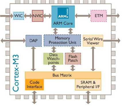
Fig.2. Cortex-M3 Processor (Source:
Cortex-M3 processors unlike legacy cores which allow on the fly changing of endianness, only have fixed endianness and only support the Thumb Instruction Set. Cortex-M3s do not come in multicore configurations but however support optional Memory protection unit.
ARM Cortex- M3 cores are used in NXP LPC 13000, 17000, 18000 series Microcontrollers. The Temperature logger design elucidated in this paper makes use of the NXP LPC 1768 Microcontroller.
-
IV. Temperature Monitoring and Logging System Hardware Details
The Temperature logger circuit is draw using the EAGLE Schematic Editor, an intuitive tool which allows users to create an easy-to-read representation of electronic designs. This schematic is then transitioned into the full PCB layout using EAGLE’s powerful, easy-to-use PCB layout editor. Fig. 7 below shows the schematics of the Temperature Logger Device. The major hardware components used include the following
-
• ARM Microcontroller Development Board
-
• Temperature Sensor (TMP102)
-
• LCD Screen (Nokia 5110)
-
• AA Batteries
-
• Real Time Clock (CR 2032)
-
• Push Buttons
-
• 2 Way Switch
-
A. Hardware Component Breakdown
-
1) ARM Microcontroller Development Board
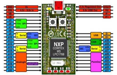
The mbed development boards are a series of ARM Microcontroller Development Boards designed for rapid prototyping. The mbed NXP LPC1768 which is used in this design and development is primarily a board of peripherals fused together with the ARM Cortex-M LPC1768 Microcontroller. One good advantage of this board is the presence of a built-in USB flash programmer which makes it easy to upload code binaries into the onboard Microcontroller flash memory. It is widely used, due to its adaptability for designing and prototyping all sorts of devices, especially those including Ethernet, USB, and the flexibility of lots of its peripheral interfaces and FLASH memory. It is packaged as a small Dual Inline Package (DIP) which makes it usable on PCB design. Fig. 3 below show the real life representation of the ARMmbed development board.
The LPC1768 is an ARM Cortex-M3 based Microcontroller for embedded applications featuring a high level of integration and low power consumption. It represents the next generation core that offers system enhancements such as enhanced debug features and a higher level of support block integration [7]. The LPC1768 has found application in varying industrial fields, motor control, medical and lighting systems. The peripheral complement of the LPC1768 includes up to 512 kB of flash memory, 64 kB of data memory, SPI, I2C-bus interfaces, input, outputs, 8-channel 12-bit ADC, 10-bit DAC, motor control PWM and many others. For this design and development, this Microcontroller on the
ARMmbed development board is programmed using C on the ARMmbed developer site which is them further compiled into binary and then uploaded onto the device local memory through the USB bootloader.
-
2) Temperature Sensor (TMP 102)
The TMP102 break-out board digital temperature sensor is used for this design and development. It uses Inter-Integrated Circuit (I2C) Serial-to-Parallel Interface (SPI) communication protocol as a communication mechanism with the Microcontroller. With its nominal 12-bit resolution it to be able to measure temperature changes as small as 0.0625 °C.
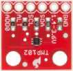
Fig.4. Temperature Sensor (TMP102)
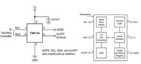
Fig.5. Temperature Sensor Typical Connection (TMP102)
The TMP102 device is two-wire, System Management Bus (SMBus) and I2C interface-compatible. When it is configured to the 13-bit data format mode (Extended Mode), it can measure temperatures ranging from –55°C to 150°C. Considering the fact that the TMP102 is acting as a slave in this application, its address is determined by where the Pin 4 (ADD0) is connected to. The various address of the TMP102 based on the Pin 4 connection are
Table 3. Table Showing Varying TMP102 Addresses Based On ADD0 Pin Connection
|
ADD0 Connection |
TMP 102 Address in Binary |
TMP 102 Address in Hexadecimal |
|
GND |
1001000 |
0x48 |
|
V+ |
1001001 |
0x49 |
|
SDA |
1001010 |
0x4A |
|
SCL |
1001011 |
0x4B |
3) Liquid Crystal Display (Nokia 5110)
A liquid-crystal display (LCD) is a flat-panel display that uses the light-modulating properties of liquid crystals. Liquid crystals do not emit light directly [8]. These LCDs are made with either passive matrix or an active matrix display grid. The passive matrix LCDs have grids of conductors with pixels located at each intersection in the grid. Current is sent across two conductors on the grid (row and column) to control the light for selected pixels. However, active matrix makes use of transistors, thereby requiring less current to control the luminance of a pixel. The Nokia 5110 LCD used in this design and development represents typical active matrix graphic LCD (Thin Film Transistor technology). Its pixels can be manipulated to draw graphics, rather than just regular texts at a low power consumption rate and at a better response rate. The Nokia 511o LCD used has the capacity to store 48 by 84 pixels in total.
The Nokia 5110 Graphical LCD package has 2 parallel 8-Pin headers above and below it. As you may be able to tell by the faint traces connecting them, each pin on one header is connected to the parallel pin on the other side. Here are the eight unique pins along with an overview of their purpose.
Table 4. Table showing the Pins of the Nokia 5110 LCD and their functions highlighted in table 3 below.
|
PIN NUMBER |
PIN LABEL |
PIN FUNCTION |
NOTES |
|
1 |
VCC |
Positive power supply |
Supply range is between 2.7V and 3.3V |
|
2 |
GND |
Ground |
|
|
3 |
SCE |
Chip select |
Active low. The enable pin allows data to be clocked in. It is typically active low |
|
4 |
RST |
Reset |
This signal will reset the device and must be applied to properly initialize the chip. The signal is active LOW |
|
5 |
D/C |
Mode select |
The input to select between command/address mode (low) and data mode (high). |
|
6 |
DN(MOSI) |
Serial data in |
Input for the data line |
|
7 |
SCLK |
Serial clock |
Input for the clock signal: 0.0 to 4.0 Mbits/s. |
|
8 |
LED |
LED backlight supply |
Acceptable voltage is between 2.7 to 3.3 V. |
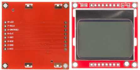
Fig.6. Nokia 5110 Graphical LCD (Bottom and Top View)
-
4) Real Time Clock (RTC)
A real-time clock (RTC) is an ultra low power back-up battery computer clock that is used to keeps track of the current time in most embedded computer devices. This frees the main system from routine time counting and makes it available for more time-critical tasks. RTCs typically make use of 32.768 kHz crystals to create clock signals which can be accurately interpreted into time frames in seconds. The frequency 32768 Hz is commonly used because it is a power of 2 (2^15) and users can precisely get 1-second interval counts from it by making use of a 15 stage binary counter. It is important to note that RTC uses UNIX time which describes time by counting the number of seconds that have elapsed since 1st January, 1970. The alternative source of power for the RTC helps to keep it running even while the primary source of power is off or unavailable. This alternate source of power is normally a lithium battery. In this design and development, the RTC is accessed by the Microcontroller through serial communication.
-
5) Two-Way Switch
The two-way switch is used in this design and development to switch ON and OFF the logging operation of the temperature logger. When switched ON, the device automatically logs the temperature reading into ‘LOGGER.csv’ file created in the local memory of the ARMmbed. These Two-Way switches are also called Single Pole Double Throw (SPDT) switches. This is because they have three terminals: one common pin and two pins which vie for connection to the common. Change in position of the switch creates corresponding changes to the state of the Microcontroller pin connected to it. By monitoring this microcontroller pin state, changes can be triggered regarding the logging operations.
-
6) Push Button
These kinds of switches are used to controls the openness or closed-ness of an electric circuit by limiting the flow of current momentarily or permanently. The momentary push button switches are used in design. These switches maintain their state continually and only toggle states when they are currently pressed. Interestingly and for ease of interactions, these switches have click feedback when pressed.
-
7) AA Batteries
These are 1.3 to 1.5 V external sources of power used by the circuit to power up the ARMmbed and the other electrical and electronic components present.
-
B. Schematic and PCB
Fig. 7, 8 and 9 below show the schematic representation of the Temperature Logger and its PCB translation. It can be seen from the schematic that the TMP102 sensor’s SDA and SCL pins are connected to the Microcontroller’s I2C SDA and SCL pins respectively. The Nokia 5110 LCD uses the Serial Peripheral Interface (SPI).
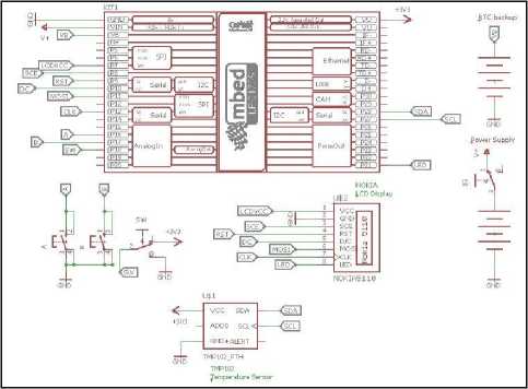
Fig.7. Schematic of the Temperature Logger Circuit
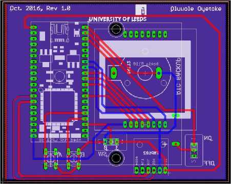
Fig.8. Temperature Logger PCB Layout (Top View)
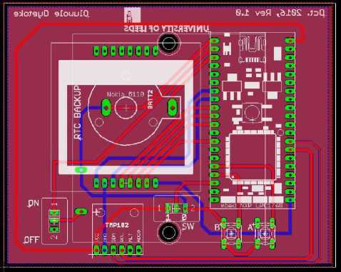
Fig.9. Temperature Logger PCB Layout (Bottom View)
-
V . Temperature Monitoring and Logging System Software Details
The online compiler available on the ARMmbed Operating System (OS) developer site is used to program the onboard MCU. This online workspace allows embedded C code to be written and compiled into their binary versions instantaneously. The ARMmbed development board (NX LPC1768) is designed in such a way that these generated binaries can be immediately loaded into the Microcontroller memory through the onboard USB.
Considering the fact that the ARMmbed NX LPC1786 is designed with an onboard mini-USB port, when the development board is connected to the computer through this port, the generated binary file from the online compiler can be copied and pasted into the file system and then when the reset button on the development board is pressed, the ARMmbed restarts operation and selects the binary file in its file system with the most recent date of creation
|
Connect ARMmbed to PC through USE port |
Write code on Mbed developer site |
Compile code to binaiy format |
||||
|
Press reset button on the Mbed to load in the new binary |
< |
Copy and paste binaiy file into Mbed file svstem |
*-l |
|||
Fig.10. Block Diagram Showing the Mbed Programing Process
The Temperature Logger has 4 components which require programming/configuration in one way or the other. These programmable components include
-
• Nokia Graphical LCD (N5110)
-
• Temperature Logger TMP102
-
• Real Time Clock
-
• LPC NX1768 Microcontroller
The Microcontroller which is the brain of the whole system is programmed to initialize and configure the temperature sensor (TMP102) at start up, receive periodic temperature updates from the sensor and displays this temperature reading either in numeric format or in temperature-vs-time graph plot on the connected graphical LCD screen (Nokia 5110 LCD).
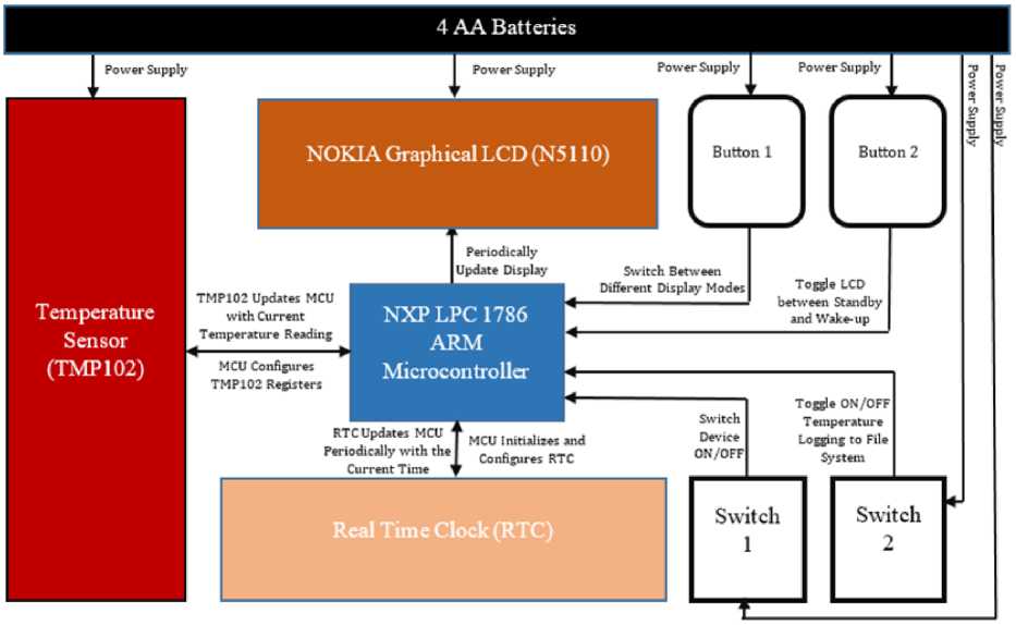
Fig.11. Block Diagram of Temperature Logger Key Component Interaction
The Microcontroller is also programmed to initialize and configures the Real Time Clock which in turn returns the current time reading every second to the Microcontroller. The Microcontroller then passes this value for display on the graphical LCD screen.
It is important to note that the communication protocol which is known as I2C (Inter-Integrated Circuit) is used for communication between some of the peripheral devices and the Microcontroller. This include the temperature sensor and the microcontroller. The block diagram shown if Fig. 11 below explains how each of these devices is programmed to interact with each other.
-
A. Microcontroller-to-Temperature Sensor Interaction
In this design and development, the Microcontroller communicates with the temperature sensor (TMP102) using a serial communication protocol called I2C (InterIntegrated Circuit). The I2C bus was designed by Philips in the early 1980s to allow easy communication between components which reside on the same circuit board [10]. The original communication speed was defined with a maximum of 100 kbits per second, however, for applications which require faster communication, there exist the ‘fastmode’ which allows up to 400 kbits operations per second and also the faster ‘highspeed’ mode which accommodates about 3.4 Megabits operations per second. I2C requires just two wires, connected to the devices Serial Clock (SCL) and Serial Data (SDA) lines. Simplicity and flexibility are key characteristics that make this bus attractive to many applications and it remains one of the most widely used communication protocol. I2C basically functions on the master-slave configuration i.e., in most cases, 1 device acts as the master which then communicates with one or more other slaves by specifying their addresses.
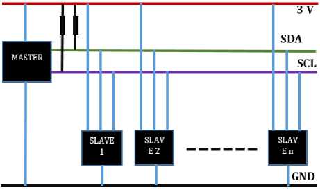
Fig.12. I2C Slave-Master Configuration
Each I2C slave has a 7-bit address, which makes a master able to communicate with up to 127 slave devices on one I2C configuration. Address ‘0x00’ is usually reserved for broadcast to all connected devices. The master is always the device that drives the SCL clock line. It is important to note that the slaves are the devices that respond to the master and cannot initiate a transfer over the I2C bus. Only a master can do that.
The transfer operation is initiated by the master by issuing a start sequence on the I2C bus. For I2C, the start and stop sequences are special in that they are the only places where the SDA (data line) is allowed to change while the SCL (clock line) is high. In fact, the start operation is triggered when the SDA changes state to low while the SCL is high while the stop command is triggered when the SDA changes state to high while the SCL is high. When data is being transferred, SDA must remain stable and not change whilst SCL is high. These start and stop sequences mark the beginning and end of a transaction with the slave device.
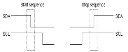
Fig.13. I2C Start and Stop Transaction Trigger
Data is transferred in sequences of 8 bits. For every 8 bits transferred, the device receiving the data sends back an acknowledge bit, so there are actually 9 SCL clock pulses to transfer each 8-bit byte of data. If the receiving device sends back a low acknowledgment (ACK) bit, then it has received the data and is ready to accept another byte. If it sends back a high ACK then it is indicating it cannot accept any further data and the master should terminate the transfer by sending a stop sequence [11].
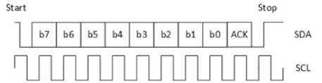
Fig.14. Timing Diagram for Sending 1 Byte Over I2C
-
1. Step by Step Analysis of the I2C Protocol Operation
-
a) Algorithm (I2C Write Operation)
At first, the master sends out a start sequence which keeps all the slave devices connected to the master through the bus on alert. The master follows this up by sending over the address of the specific slave it intends to communicate with. The slave that matches this address will continue with the transaction while the others will ignore the rest of this transaction and wait for the next start sequence. After these successful match between the master and the slave, the master is required to send out the internal location or register address inside the slave that it wishes to interact with
-
1) Send a start sequence
-
2) Send the I2C address of the slave with the R/W bit set to low
-
3) Send the internal register address
-
4) Send the data byte
-
5) [Optionally, send any further data bytes]
-
6) Send the stop sequence.
-
b) Algorithm (I2C Read Operation)
Reading from the slave is a bit different. a read of the slave starts off by writing to it. The start sequence is sent with the R/W bit of the address set to low. This is then followed by the address of the internal register that would be written to. Since this is a read operation, another start sequence i.e. restart is sent, this time with the read bit set to high. This can then be followed by as many read operations needed which can later be terminated with the stop sequence.
-
1) Send a start sequence
-
2) Send I2C address of the slave with the R/W bit low
-
3) Send Internal register’s address
-
4) Send a start sequence again (repeated start)
-
5) Send I2C address of the slave with the R/W bit
high
-
6) Read as many data bytes from the slave device as needed
-
7) Send the stop sequence.
-
2. Initializing and Configuring the TMP102
The address of the TMP102 is dependent on the connection of its ‘ADD0’ pin. Table 5 below shows the various possible addresses of the TMP102 with respect to its ‘ADD0’ pin connection.
Table 5. Table showing Possible TMP102 Addresses
|
S/N |
ADD0 Connection |
TMP102 Address |
TMP102 Read Address (Binary) |
TMP102 Read Address (Hex) |
TMP102 Write Address (Binary) |
TMP102 Write Address (Hex) |
|
1 |
Ground |
1001000 |
10010001 |
0x91 |
10010000 |
0x90 |
|
2 |
V+ |
1001001 |
10010011 |
0x93 |
10010010 |
0x92 |
|
3 |
SDA |
1001010 |
10010101 |
0x95 |
10010100 |
0x94 |
|
4 |
SCL |
1001011 |
10010111 |
0x97 |
10010110 |
0x96 |
The TMP 102 has 4 internal registers which take on different functions. These registers include:
-
1) Temperature Register
-
2) Configuration Register
-
3) TLOW Register
-
4) HIGH Register
-
5) Pointer Register
-
a) Pointer Register
This is an 8-bit register used to determine what data register must respond to a read or write command. It uses the two least-significant bits (LSBs) to determine this. Table 6 and 7 below elaborates on how this register is structured.
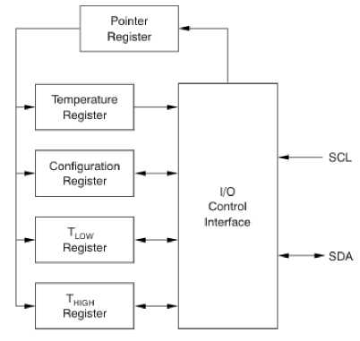
Fig.15. TMP102 Internal Registers (Source: TMP102 Data Sheet [12])
Table 6. Table depicting Pointer Register memory
|
P7 |
P6 |
P5 |
P4 |
P3 |
P2 |
P1 |
P0 |
|
0 |
0 |
0 |
0 |
0 |
0 |
Reg. pointer bits |
|
Table 7. Pointer Register Location Pointer Based on Inputs
|
P1 |
P0 |
Register Pointed to |
|
0 |
0 |
Temperature Register (Read Only) |
|
0 |
1 |
Configuration Register (Read/Write) |
|
1 |
0 |
TLOW Register (Read/Write) |
|
1 |
1 |
THIGH Register (Read/Write) |
-
b) Configuration Register
The Configuration Register is a 16-bit read/write register used to store bits that control the operational modes of the temperature sensor. Read/write operations are performed MSB first [12].
Table 8. TMP102 Configuration Register Memory Space
|
BY TE 1 |
Position |
D7 |
D6 |
D5 |
D4 |
D3 |
D2 |
D1 |
D0 |
|
Label |
OS |
R1 |
R0 |
F1 |
F0 |
POL |
TM |
SD |
|
|
Content |
0 |
1 |
1 |
0 |
0 |
0 |
0 |
0 |
|
|
BY TE 2 |
Position |
D7 |
D6 |
D5 |
D4 |
D3 |
D2 |
D1 |
D0 |
|
Label |
CR1 |
CR0 |
AL |
EM |
0 |
0 |
0 |
0 |
|
|
Content |
1 |
0 |
1 |
0 |
0 |
0 |
0 |
0 |
The contents 0b01100000 and 0b10100000 of the configuration register in Table 8 above is the normal reset value. However, for this design and development, 0b01111000 and 0b01100000 are used for Byte 1 and 2 respectively, so as to satisfy some of the performance requirement of the device such as less frequent temperature conversion. The sections below explain the importance of each of the registry space present in the TMP102 Configuration Register memory
Shutdown Mode (SD): The configuration register memory position with the label (SD) is used to toggle between continuous temperature conversion state and a non-continuous mode whereby all device circuitry is shut down when the current conversion is complete. For this design and development, SD is set to 0, thereby maintaining a continuous conversion method.
Thermostat Mode (TM): The configuration register memory position with the label (TM) is used to toggle between Comparator (TM = 0) and Interrupt Mode (TM=1). For this design and development, TM is set to 0.
Polarity (POL): The configuration register memory position with the label (POL) is used to set the polarity of the alert pin. If POL=1, ALERT pin becomes active high and vice versa. For this design and development, POL is set to 0
Fault Que (F1/F0): The configuration register memory position with the label (F1 and F0) are used to programme the number of fault occurrence required before an alert is triggered. Faults usually happen when the measured temperature exceeds the user-defined limits in THIGH or TLOW Registers. For this design and development, F1 and F0 are set to – 1 and 1 respectively
Table 9. Various Configuration for TMP102 Configuration Register Fault Settings
|
F1 |
F0 |
No. of Faults to Trigger Alert |
|
0 |
0 |
1 |
|
0 |
1 |
2 |
|
1 |
0 |
4 |
|
1 |
1 |
6 |
Converter Resolution (R1/R0): The configuration register memory position with the label R1 and R0 are used to set the conversion resolution of the device. For this design and development, R1 and R0 are set to 1 and 1 respectively. This gives the device a 12-bit resolution. The 12-bit resolution allows the tmp102 to be able to detect and represent temperature changes as minute as 0.0625 oC
One Shot: The configuration register memory position with the label (OS) is used to achieve a ‘do it when I need it’ kind of temperature conversion approach. When the device is in Shutdown Mode, writing a 1 to the OS bit starts a single temperature conversion. During the conversion, the OS bit reads '0'. The device returns to the shutdown state at the completion of the single [12]. For this design and development, OS is set to –
Extended Mode (EM): The configuration register memory position with the label (EM) is used to determine the data format that will be used by the temperature register TLOW and THIGH registers. When EM=0 (Normal mode), these registers make use of the 12-bit data format. However, when EM=1 (Extended mode), the 13-bit data format is used for this design and development, EM is set to 0.
Alert (AL): The configuration register memory position with the label AL is used to provide information on the comparator and interrupt mode status. For this design and development, AL is set to 1
Conversion Rate (CR): The configuration register memory position with the label CR1 and CR0 are used to set the number of times in a second, the TMP102 should carry our temperature reading/conversion. Table 9 below explains various contents combination in this register location and their effects. For this design and development, CR1 and CR0 are set to 0 and 1 respectively.
Table 10. Various CR1 and CR0 combinations and their effects
|
CR1 |
CR0 |
Conversion Rate (Hz) |
No of Conversions Per Second |
|
0 |
0 |
0.25 |
(Every 4 Seconds) |
|
0 |
1 |
1 |
1 |
|
1 |
0 |
4 |
4 |
|
1 |
1 |
8 |
8 |
-
c) Temperature Register
This is a 12/13 bit read-only register used to store current temperature conversion value. When the EM position of the configuration register is set to 1, this register switches to the 13-bit mode. This can be switched back to the 12-bit mode by changing the EM bit to 0. For this design and development, the 12-bit data format is used. The register slot normally contains 2 bytes of data, however, only the first 12/13 represent the current temperature reading. With the 12-bit temperature data format, temperatures ranging from -55 oC to +128 oC can be read. Also, for the 13-bit temperature data format, temperatures ranging from -55 oC to +150 oC can be read. Table 11 below shows the various binary values for different temperature conversions. Note that the negative temperature readings are derived by performing the twos compliment of their corresponding positive value.
Table 11. 12-bit Data Format Temperature Conversion Values
|
Temperature in Decimals ( o C) |
Temperature in Binary |
Temperature in Hex |
|
128 |
0111 1111 1111 |
7FF |
|
100 |
0110 0100 0000 |
640 |
|
25 |
0001 1001 0000 |
190 |
|
. . . |
. . . |
. . . |
|
-25 |
1110 0111 0000 |
E70 |
|
-55 |
1100 1001 0000 |
C90 |
Performing the Twos compliment
The twos compliment is performed by inverting the original binary values and adding 1 to the answer. For example, to derive -25:
-
• +25 = 000110010000 in binary.
-
• When inverted, it becomes 111001101111.
-
• Adding a one to the inverted answer will translate to 111001110000
Converting the Temperature Reading to Decimal
The Byte 1 of the temperature register represents the most significant sets of bits and in this design, only the last for bits of the byte one and the first 4 bits of the byte 0 are read. In order to do this, bit shifting is carried out. Considering the fact that when bits are shifted in a binary array, they fall off when they get to the edges, therefore transformation.
The integer value of the resulting binary value as above is then multiplied by the temperature resolution which is 0.0625 in this case, to obtain the actual decimal value of the temperature. Function ‘readTemperature()’ of the controller code in Appendix A is used to perform the temperature reading operation
-
d) High and Low Limit Registers (THIGH & TLOW)
-
3. Implementing A Ticker for the Temperature Read Operation
The temperature limits are stored in the T (LOW) and T (HIGH) registers in the same format as the temperature result, and their values are compared to the temperature result on every conversion. The outcome of the comparison drives the behaviour of the ALERT pin, which operates as a comparator output or an interrupt, and is set by the TM bit in the configuration register [12].
In order to make sure that the temperature reading function (‘readTemperature()’) only operates once every 60 seconds, a ticker is utilized. The Ticker interface is used to setup a recurring interrupt to repeatedly call a function at a specified rate. Any number of Ticker objects can be created, allowing multiple outstanding interrupts at the same time [13]. To implement the ticker, a ticker object is first of all created and then in the main method, the temperature reader function is then attached to the ticker object. Lines 72 and 368 of the controller code in Appendix A gives full details of this process
-
B. Microcontroller-to-Graphical LCD Interaction
The graphical LCD used in this design is the Nokia 5110 LCD. This is used in complement with a customized library developed by Craig. C. Evans (the University of Leeds Electronic and Electrical Engineering Lecturer). The open source library present on the ARMmbed developer site provides functions which help in displaying text on the LCD as well as manipulating the LCD’s 48 by 84 available pixel spots in drawing graphs. The LCD is initially initialized and subsequently, its display is changed in accordance with the current display mode specification (view/write mode or plot mode).
-
C. Microcontroller-to-Real Time Clock Interaction
The real time clock is initially configured with the use of a virtual serial terminal on a PC. The Universal Asynchronous Receiver/Transmitter (UART) controller is the key component of the serial communications between a device and a computer or between devices in general. It changes incoming parallel information from within the Microcontroller or Computer to serial data which can be sent on a communication line [14]. The periodic reading of the time and update of the LCD is achieved by attaching the ‘updateLCDtime’ function to the ‘timeInterval’ ticker object which is initialized to interrupt every 1 second.
-
D. Microcontroller-to-Switch & Push Button Interaction
Switch 1, button A and B are connected to pin 18, 16 and 17 of the MCU respectively. In order to provide override capability and make sure a process interrupt happens whenever the buttons connected to this pins are pushed, Interrupts are set on PIN 16 and 17 by creating objects of the Input Interrupt Class. These interrupt objects are now assigned specific functions which must be fired whenever these interrupts are triggered. the function used to place the LCD on standby/wake mode is attached to the interrupt on pin 17 while the function used to switch the display between ‘view/write mode’ and ‘plot mode’ is attached to the interrupt on pin 16. Switch 1 is used to toggle ON and OFF the logging operation.
-
E. Code Analysis
-
1. Class Diagram
In software engineering, a class diagram is a type of static structure diagram that describes the structure of a system by showing the system's classes, their attributes, operations (or methods), and the relationships among objects [15]. Class diagrams can also be used for data modelling [16].
-rxString[16] : char
-setTimeFlag : int
-setLogFlag :int
-setPlotFlag : int
-LCDStanbyFlag=0 : int
-temperatureValue = 0 : float
-tempValueDispBuffer[14] : char
-timeValueDispBuffer[30] : char
-dateValueDispBuffer[30] : char
-datetimeValueDispBuffer[30] : char
-local("local") : LocalFileSystem
-ErrorBuzzer(code : int): void
-initializeTMP102(): void
-main(): int
-plot(): void
-readTemperature(): void
-serialISR(): void
-setTime(): void
-standbyFunction(): void
-
- trigerViewChange(): void
-
- updateLCDTime(): void
-writeDataToFile(data : int): void
-
2. Code Flow
-
3. Function Break Down
Fig.16. Class Diagram of the C Programme Running on the Microcontroller
The flow chart in Fig. 17 below depicts the flow of instructions and operation carried out by the ARMmbed
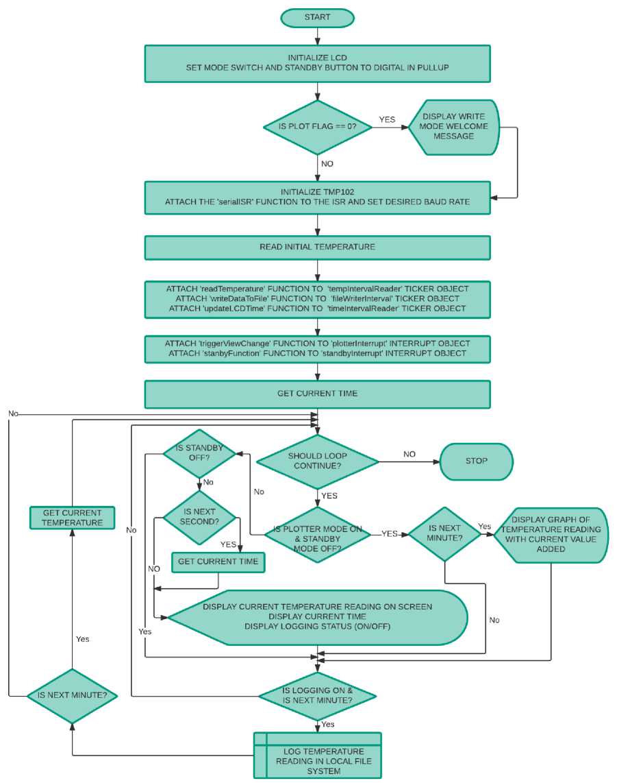
Fig.17. The Flowchart Showing the Flow of the C Programme Running on the ARMmbed Microcontroller
Overall, there are 11 functions working hand in hand with the main function. These functions are as identified in the class diagram in section 3.5.1. The sections below explain the operation of each of these functions
-
a) Error Indicator Function [ErrorBuzzer(code : int): void]
This function is used to trigger on the ARMmbed LEDs whenever an error occurs. Based on the combination of blinking LEDs, the occurring error can be deciphered. This is because the method receives an integer value between 0 and 15 which represents the error label. The combination of four LEDs that make up this number are/is then lit up.
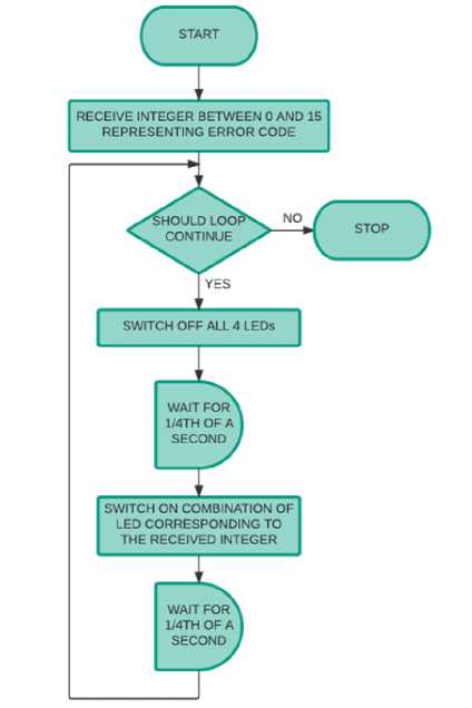
Fig.18. The Flowchart Explaining the Flow of Operation of the ‘ErrorBuzzer’ Function
-
b) Temperature Sensor Initializer Function
[initializeTMP102(): void]
This function is used to initialize the TMP102 sensor. Primarily to set its bus speed and configure its configuration register to make its operation suitable for the desired need and stated specifications. Fig. 19 below represents the flow of operation of the function.
-
c) Plotter Function [plot(): void]
This function is used to plot the temperature reading against time, momentarily on the graphical LCD
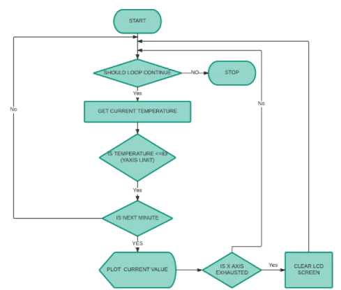
Fig.20. The Flowchart Explaining the Flow of Operation of the ‘plot’ Function
-
d) Temperature Reader Function [readTemperature(): void]
This function is used to read the instantaneous temperature value present in the TMP102 temperature register.
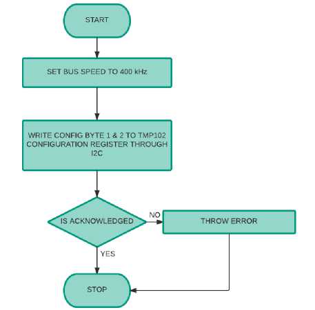
Fig.19. The Flowchart Explaining the Flow of Operation of the ‘initializeTMP102’ Function
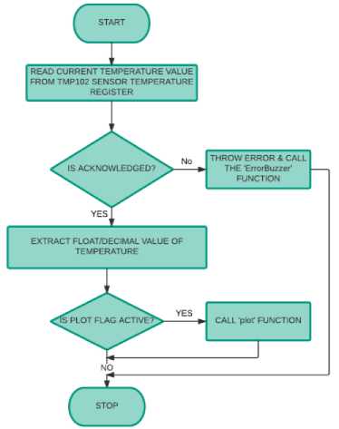
Fig.21. The Flowchart Explaining the Flow of Operation of the ‘readTemperature’ Function
-
e) Serial Link Interrupt Service Routine [serialISR(): void]
This function is used to capture streams of data on the serial interface whenever a PC serial connection is discovered.
-
f) Set Time Function [setTime(): void]
This function is used to set the Real Time Clock (RTC) via the serial connection.
-
g) Standby Function [standbyFunction(): void]
This function is attached to an interrupt and triggered at the press of push-button B. When triggered, it checks the ‘LCDStanbyFlag’ to determine if to switch OFF the LCD or switch it ON. When this function is triggered, if the current LCDStandbyFlag==0, the LCD is switched OFF, LCDStandbyFlag==1 and subsequent push of the button will do vice versa.
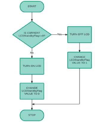
Fig.22. The Flowchart Explaining the Flow of Operation of the ‘standbyFunction’ Function
-
h) View Change Function [trigerViewChange(): void]
This function is used to trigger view change on the LCD, between the writing value mode to the value plotter mode. The function first of all checks the ‘setPlotFlag’ to determine the current mode. If the current value of the ‘setPlotFlag’ is 0, the view on the LCD is immediately changed to the plot view and ‘setPlotFlag’ is set to 1. If ‘setPlotFlag’ is 1, a reverse operation is performed. If the plot mode is activated, the function also draws the x and y-axis lines before the temperature plots begin to take place.
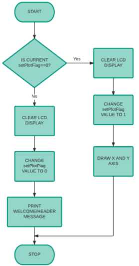
Fig.23. The Flowchart Explaining the Flow of Operation of the ‘triggerViewChange’ Function
-
i) Update LCD Time Function [updateLCDTime(): void]
This function is attached to the ‘timeIntervalReader’ ticker which triggers the function to run every second. The function gets the current UNIX time value from the RTC clock, then formats it into a string for display and then displays the time, if the current view mode is the ‘write mode’. Time updates are not shown on the ‘plot mode’, so as to maximize screen capacity. The flow chart shown in Fig. 28 below explains the flow of operation of this function.
-
j) Write Data To Local File System [writeDataToFile(data : int): void]
This function is attached to the ‘fileWriteInterval’ ticker object which triggers a write to local file system operation once every 60 seconds, as long as logging is switched ON using the switch B. The function is structured to trigger the ARMmbed’s LEDs to flash during write operations. It switches on the 4 LEDs, checks that logging is switched on, opens the local file system, formats the current temperature reading and time update into a single string which is comma delimited, writes the string into the local file system, closes the file and then switches OFF the LEDs, thereby producing a brief flashing effect.
-
VI. Result and Testing
For improved user-friendly interactivity, the LEDs on the ARMmbed are programmed to flash during the ‘write to file system’ operation and by shifting the Switch 1 accordingly, the user can toggle ON/OFF the logging operation. The logging status is normally shown on the row 6 of the LCD screen while in the write/view mode.
Through the use of a the ARMmbed’s ticker functionality, the Temperature Logging and Monitoring device is successfully designed and programmed to update temperature readings and log them every 60 seconds. One ticker object is used to update time every second while the other is used to update the temperature reading every 60 seconds. At the 60th second, the logger object triggers the temperature logging function which then formats the current time and temperature reading appropriately (e.g. ‘09:06 7/8/14 , 27.54’) and logs them into the created .csv file in the file system.
By pressing the push button A, the user can switch from the write/view mode to the plot mode where by the graphical plot of the cumulative temperature reading against time is displayed as can be seen in Fig. 26.
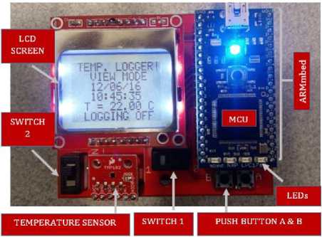
Fig.24. Labeled Snapshot of Temperature Logger on Write/View Mode, Logging OFF
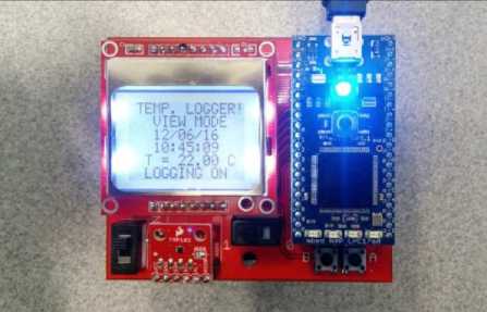
Fig.25. Snapshot of Temperature Logger on Write/View Mode, Logging ON
To conserve energy usage, push button B is used to place the LCD screen on standby. This standby will persist, even while the logging operation continues. Although the Temperature Logger can be powered through the ARMmbed’s USB port, the circuit is also connected to back-up batteries which can power the circuitry directly. Switch 2 is used in this case to switch this power ON and OFF
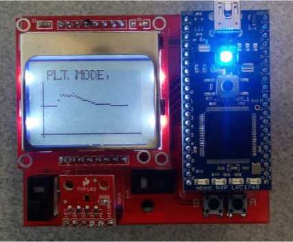
Fig.26. Snapshot of Temperature Logger on Plot Mode 1
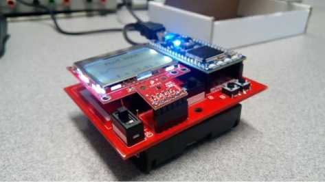
Fig.27. Snapshot of Temperature Logger (Top Side View)
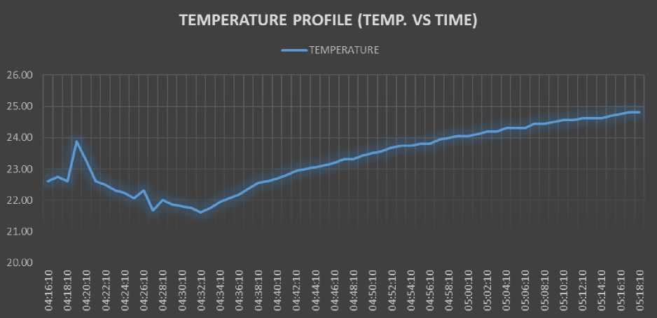
The Temperature Logger is switched on and allowed to take temperature reading for about 62 minutes. Table 12 below shows the content of the ‘LOGGER.CSV’ file. This file can be copied and its content (time and temperature reading) is plotted against each other. Fig. 28 below depicts the temperature profile for the 62 minutes of running.
Table 12. The Content of the .CSV File Containing the Logged Values in the Temperature Logger Local File System
|
TIMESTAMP |
TEMPERATURE ( O C) |
|
12/06/2016 04:16:10 |
22.62 |
|
12/06/2016 04:17:10 |
22.75 |
|
12/06/2016 04:18:10 |
22.62 |
|
12/06/2016 04:19:10 |
23.88 |
|
12/06/2016 04:20:10 |
23.25 |
|
12/06/2016 04:21:10 |
22.61 |
|
12/06/2016 04:22:10 |
22.50 |
|
12/06/2016 04:23:10 |
22.31 |
|
12/06/2016 04:24:10 |
22.25 |
|
12/06/2016 04:25:10 |
22.06 |
|
12/06/2016 04:26:10 |
22.31 |
|
12/06/2016 04:27:10 |
21.68 |
|
12/06/2016 04:28:10 |
22.00 |
|
12/06/2016 04:29:10 |
21.88 |
|
12/06/2016 04:30:10 |
21.81 |
|
12/06/2016 04:31:10 |
21.75 |
|
12/06/2016 04:32:10 |
21.62 |
|
12/06/2016 04:33:10 |
21.75 |
|
12/06/2016 04:34:10 |
21.94 |
|
12/06/2016 04:35:10 |
22.06 |
|
12/06/2016 04:36:10 |
22.19 |
|
12/06/2016 04:37:10 |
22.38 |
|
12/06/2016 04:38:10 |
22.56 |
|
12/06/2016 04:39:10 |
22.62 |
|
12/06/2016 04:40:10 |
22.69 |
|
12/06/2016 04:41:10 |
22.81 |
|
12/06/2016 04:42:10 |
22.94 |
|
12/06/2016 04:43:10 |
23.00 |
|
12/06/2016 04:44:10 |
23.06 |
|
12/06/2016 04:45:10 |
23.12 |
|
12/06/2016 04:46:10 |
23.19 |
|
12/06/2016 04:47:10 |
23.31 |
|
12/06/2016 04:48:10 |
23.31 |
|
12/06/2016 04:49:10 |
23.44 |
|
12/06/2016 04:50:10 |
23.50 |
|
12/06/2016 04:51:10 |
23.56 |
|
12/06/2016 04:52:10 |
23.69 |
|
12/06/2016 04:53:10 |
23.75 |
|
12/06/2016 04:54:10 |
23.75 |
|
12/06/2016 04:55:10 |
23.81 |
|
12/06/2016 04:56:10 |
23.81 |
|
12/06/2016 04:57:10 |
23.94 |
|
12/06/2016 04:58:10 |
24.00 |
|
12/06/2016 04:59:10 |
24.06 |
|
12/06/2016 05:00:10 |
24.06 |
|
12/06/2016 05:01:10 |
24.12 |
|
12/06/2016 05:02:10 |
24.19 |
|
12/06/2016 05:03:10 |
24.19 |
|
12/06/2016 05:04:10 |
24.31 |
|
12/06/2016 05:05:10 |
24.31 |
|
12/06/2016 05:06:10 |
24.31 |
|
12/06/2016 05:07:10 |
24.44 |
|
12/06/2016 05:08:10 |
24.44 |
|
12/06/2016 05:09:10 |
24.50 |
|
12/06/2016 05:10:10 |
24.56 |
|
12/06/2016 05:11:10 |
24.56 |
|
12/06/2016 05:12:10 |
24.62 |
|
12/06/2016 05:13:10 |
24.62 |
|
12/06/2016 05:14:10 |
24.62 |
|
12/06/2016 05:15:10 |
24.69 |
|
12/06/2016 05:16:10 |
24.75 |
|
12/06/2016 05:17:10 |
24.81 |
|
12/06/2016 05:18:10 |
24.81 |
TEMPERATURE PROFILE (TEMP. VS TIME)
TEMPERATURE
Fig.28. Graph Showing the Temperature Profile Based on Logged Temperature Stored On the Logger Local File System
-
VII. Conclusion
Embedded Systems are indeed the future of our technology-oriented world. Details from this report show clearly the chemistry involved when hardware and software fuse together to bring about innovative solutions which interestingly have numerous applications in varying spheres of life.
With the help of the ARMmbed developer site, the ARM NXP LPC 1768 Microcontroller is programmed to carry out dedicated and specific tasks, even as it serves its place as just one out of the many other components on the Printed Circuit Board. The Microcontroller efficiently interacts with the TMP102 to retrieve current temperature readings, format these readings for appropriate display on the graphical LCD. The Microcontroller also interacts every second with the RTC to retrieve current time update which is then converted from their UNIX representation to strings suitable for display. These time and current temperature readings are not only displayed on the LCD, but are also logged into a CSV file on the local file system of the ARMmbed development board. The logging operation can be switched ON/OFF while the LCD standby mode can also be triggered by an interrupt. In addition, for better view and perspective, the display mode can be switched from written text to a plot mode whereby the temperature reading is plotted over the current time period
Considering the fact that the Internet of Things (IoT) has become a part of our everyday life, this design can be expanded by including web interactivity. The wide range of possible applications of embedded controllers makes it no surprise that they are now present in millions of devices around the globe. Recent research showed that the typical new-model vehicle comes with over 100 million lines of code [17] and these numbers remain ever increasing. The utilization of the ARM Cortex-M3 processor core in the development of the Temperature Monitoring and Logging System shows a succinct application of embedded controllers and ultimately provides a full cycle hands on experience of the processes involved in engineering embedded systems/devices, especially using ARM processor-based microcontrollers
Appendix A– Embedded C Code Excerpt
//INTRODUCTION /*‐‐‐‐‐‐‐‐‐‐‐‐‐‐‐‐‐‐‐‐‐‐‐‐‐‐‐‐‐‐‐‐‐‐‐‐‐‐‐‐‐‐‐‐‐‐‐‐‐‐ Author: Oluwole O. Oyetoke
SUMMARY: This code is written to run on the ARMmbed LPC1768 board. It is developed to configure the board which is connected to a TMP102 to constantly measure temperature, update the display every minute and also plot these values over time on the LCD ‐‐‐‐‐‐‐‐‐‐‐‐‐‐‐‐‐‐‐‐‐‐‐‐‐‐‐‐‐‐‐‐‐‐‐‐‐‐‐‐‐‐‐‐‐‐‐‐‐‐*/
#include
//Define slave address for different conditions //ADD0 of TMP102 is connected to ground... address will be Ob1001000 = 0x48
#define slaveAddress 0x48
#define slaveWriteAddress 0x90
#define slaveReadAddress 0x91
/*Define needed register addresses
‐‐‐‐‐‐‐‐‐‐‐‐‐‐‐‐‐‐‐‐‐‐‐‐‐‐‐‐‐‐‐‐‐‐‐‐‐‐‐‐‐‐‐‐‐‐‐‐‐‐‐| |BIT FUNCTION| P7 | P6 | P5 | P4 | P3 | P2 | P1 | P0
| BYTE 1 | 0 | 0 | 0 | 1 | 1 | 0 | 0 | 0
|‐‐‐‐‐‐‐‐‐‐‐‐‐‐‐‐‐‐‐‐‐‐‐‐‐‐‐‐‐‐‐‐‐‐‐‐‐‐‐‐‐‐‐‐‐‐‐‐-‐| P1 P0 REGISTER
0 0 TEMPERATURE REGISTER (Read Only)
0 1 CONFIGURATION REGISTER (Read/Write)
1 0 TLOW REGISTER (Read/Write)
1 1 THIGH REGISTER (Read/Write)
*/
#define tempRegAddress 0x00 //0b00000000
#define configRegAddress 0x01; //0b00000001
#define tlowRegAddress 0x02; //0b00000010
#define thighRegAddress 0x03; //0b00000011
//‐‐‐‐‐‐‐‐‐‐‐‐‐‐‐‐‐‐‐‐‐‐‐‐‐‐‐‐‐‐‐‐‐‐‐‐‐‐-‐‐‐‐‐‐‐‐‐‐‐
//PIN CONNECTION SET‐UP
//‐‐‐‐‐‐‐‐‐‐‐‐‐‐‐‐‐‐‐‐‐‐‐‐‐‐‐‐‐‐‐‐‐‐‐‐‐‐‐‐‐‐‐‐‐‐‐‐‐ //Set pin connection to LCD
N5110 lcd(p7,p8,p9,p10,p11,p13,p21);
//Set pin connection for the TMP102 I2C tmp102(p28, p27); //p28‐SDA, p27‐SCL
//Set pins for error display leds
BusOut myleds(LED1, LED2, LED3, LED4);
//Set pins for USB connectivity
Serial pc(USBTX,USBRX); //Usually (p9,p10) for external devices
//Set logging control pin
DigitalIn loggerSwitch(p18);
DigitalIn plotterModeButton(p16);
DigitalIn standbyButton(p17);
//Set interrupt on pin 16 and 17
InterruptIn plotterInterrupt(p16);
InterruptIn standbyInterrupt(p17);
//‐‐‐‐‐‐‐‐‐‐‐‐‐‐‐‐‐‐‐‐‐‐‐‐‐‐‐‐‐‐‐‐‐‐‐‐‐‐‐‐‐‐‐‐‐‐‐‐‐
//DEFINE NEEDED OBJECTS
//‐‐‐‐‐‐‐‐‐‐‐‐‐‐‐‐‐‐‐‐‐‐‐‐‐‐‐‐‐‐‐‐‐‐‐‐‐‐‐‐‐‐‐‐‐‐‐‐‐ Ticker tempIntervalReader, timeIntervalReader, fileWriteInterval;
//‐‐‐‐‐‐‐‐‐‐‐‐‐‐‐‐‐‐‐‐‐‐‐‐‐‐‐‐‐‐‐‐‐‐‐‐‐‐---‐‐‐‐‐‐‐‐‐
//FUNCTION TO UPDATE LCD WITH NEW TIME READING //‐‐‐‐‐‐‐‐‐‐‐‐‐‐‐‐‐‐‐‐‐‐‐‐‐‐‐‐‐‐‐‐‐‐---------------- void updateLCDTime(){ time_t seconds = time(NULL); // Get current time
// Format time into a string (time and date)
strftime(timeValueDispBuffer, 30 , " %X", localtime( strftime(dateValueDispBuffer, 30 , " %x", localtime( strftime(datetimeValueDispBuffer,30 , "%x %X", localtime(&seconds));
// print time on LCD if((setPlotFlag==0)){ lcd.printString(dateValueDispBuffer,0,2); // Print on LCD lcd.printString(timeValueDispBuffer,0,3); // Print on LCD
}
}
//‐‐‐‐‐‐‐‐‐‐‐‐‐‐‐‐‐‐‐‐‐‐‐‐‐‐‐‐‐‐‐‐‐‐‐‐‐‐‐‐‐‐‐‐‐‐‐‐‐-
//SERIAL LINK INTERRUPT SERVICE ROUTINE
//‐‐‐‐‐‐‐‐‐‐‐‐‐‐‐‐‐‐‐‐‐‐‐‐‐‐‐‐‐‐‐‐‐‐‐‐‐‐‐‐‐‐‐‐‐‐‐‐‐-void serialISR() {
// set flag setTimeFlag = 1;
}
//‐‐‐‐‐‐‐‐‐‐‐‐‐‐‐‐‐‐‐‐‐‐‐‐‐‐‐‐‐‐‐‐‐‐‐‐‐‐‐‐‐‐‐‐‐‐‐‐‐-
// FUNCTION USED TO INITIATE LED FLASHING WHEN AN ERROR OCCURS
//‐‐‐‐‐‐‐‐‐‐‐‐‐‐‐‐‐‐‐‐‐‐‐‐‐‐‐‐‐‐‐‐‐‐‐‐‐‐‐‐‐‐‐‐‐‐‐‐‐‐ void ErrorBuzzer(int code)
{ while(1) { //hang in infinite loop flashing error code myleds = 0; //LEDs OFF wait(0.25); //Wait for 1/4th of a second myleds = code; //LEDs ON wait(0.25); //Wait for 1/4th of a second
}
//‐‐‐‐‐‐‐‐‐‐‐‐‐‐‐‐‐‐‐‐‐‐‐‐‐‐‐‐‐‐‐‐‐‐‐‐‐‐‐‐‐‐‐‐‐‐‐‐‐‐
//FUNCTION USED TO SET‐UP TMP102 CONFIGURATION REGISTER AS DESIRED
//‐‐‐‐‐‐‐‐‐‐‐‐‐‐‐‐‐‐‐‐‐‐‐‐‐‐‐‐‐‐‐‐‐‐‐‐‐‐‐‐‐‐‐‐‐‐‐‐‐ void initializeTMP102(){
//Set bus speed to 400kHz tmp102.frequency(400000);
int acknowledgement = 1; //Initialized to false
/*
Configure the 16 bits register structure of the configuration register
BIT FUNCTION| OS | R1 | R0 | F1 | F0 | POL|TM| SD BYTE 1 | 0 | 1 | 1 | 1 | 1 | 0 | 0|0
BIT FUNCTION| CR1 | CR0 | AL | EM | 0 | 0 | 0 |0
BYTE 2 | 0 | 1 | 1 | 1 | 1 | 0 | 0 |0
BIT FUNTION EXPLANTION
OS (ONE‐SHOT): 0 ‐‐> not in use
R1, R2 (RESOLUTION): 1, 1 ‐‐> Sets the temperature register to 12 bits
F1, F0 (FALUT QUE): 1,1 ‐‐> 6 consecutive faults before alert is triggered
POL (POLARITY): 0 ‐‐> Alert pin will be active low
TM (THERMOSTAT MODE): 0 ‐‐> Comparator mode activated
SD (SHUTDOWN MODE): 0 ‐‐> Continuous conversion. No intermittent shutdown
CR1, CR0 (CONV. RES.): 0, 1 ‐‐> 1Hz, 1 conversion per second
AL (ALERT): 1 ‐‐> Read only + only takes the opposite vaue of POL
EM (EXTENDED MODE): 0 ‐‐> Normal Mode. Sets
TREG,THIGH,TLOW reg. to 12 bts
*/ char byteOne = 0x70; //0b01111000
char byteTwo = 0x60; //0b01100000
//Initiate contact with slave, specify desired register and the data to write.
//Package contains address and the data to write char configPackage[3];
configPackage[0] = configRegAddress;
configPackage[1] = byteOne;
configPackage[2] = byteTwo;
if(acknowledgement==1){ //I2C always returns 0 for successful operation
ErrorBuzzer(1); //Error Message
}
}
//‐‐‐‐‐‐‐‐‐‐‐‐‐‐‐‐‐‐‐‐‐‐‐‐‐‐‐‐‐‐‐‐‐‐‐‐‐‐‐‐‐‐‐‐‐‐‐‐‐-
//Temperature Reader Function
//‐‐‐‐‐‐‐‐‐‐‐‐‐‐‐‐‐‐‐‐‐‐‐‐‐‐‐‐‐‐‐‐‐‐‐‐‐‐‐‐‐‐‐‐‐‐‐‐‐ void readTemperature(){ int acknowledgement=1; //Initialized to 1
char tempRegisterData[2];
int temperature = 0;
//Inititate contact with slave by trying to write to its temp register
if(acknowledgement==1){ //I2C always returns 0 for successful operation
ErrorBuzzer(2); //Error Message
}
ErrorBuzzer(3); //Error Message
} temperature = (tempRegisterData[0] << 4) |
(tempRegisterData[1] >> 4);
temperatureValue = temperature*0.0625;
if(setPlotFlag==1){ plot();
}
//return temperature*0.0625;
//float tmp =
(float((tempRegisterData[0]<<8)|tempRegisterData[1])
/ 256.0);
}
//‐‐‐‐‐‐‐‐‐‐‐‐‐‐‐‐‐‐‐‐‐‐‐‐‐‐‐‐‐‐‐‐‐‐‐‐‐‐‐‐‐‐‐‐‐‐‐‐‐
Complete code and circuit design files can be retrieved from the repositories listed belo
Mbed Developer Repository:
GitHub:
Acknowledgment
I wish to acknowledge knowledge gained from the University of Leeds Electronic and Electrical Engineering Faculty, especially Dr. Craig Evans (the Nokia N5110 library developer), Dr. Chris Trayner and David Moore.
References A Practical Application of ARM Cortex-M3 Processor Core in Embedded System Engineering
- Oluwole O. Oyetoke and Adedayo Adedapo, 'A Microcontroller Based Embedded System Design for Device Automation and Control in Intelligent Buildings', International Journal of Research (IJR), Volume 2, Issue 12, pp1,December 2015. [Online]. Available: http://internationaljournalofresearch.org. [Accessed 1st January, 2017].
- Oluwole O. Oyetoke and Adedayo Adedapo,' Embedded Systems Engineering, the Future of Our Technology World; A Look Into the Design of Optimized Energy Metering Devices', International Journal of Recent Engineering Science (IJRES). volume18, pp1 December 2015. [Online]. Available: http://jetir.org. [Accessed 1st January, 2017].
- Michael Barr; Anthony J. Massa (2006). "Introduction". Programming embedded systems: with C and GNU development tools. O'Reilly. pp. 1–2. ISBN 978-0-596-00983-0.
- Barr, Michael (1 August 2009). "Real men program in C". Embedded Systems Design. TechInsights (United Business Media). p. 2. Retrieved 2009-12-23.
- Michael Barr. "Embedded Systems Glossary". Neutrino Technical Library. Retrieved 2007-04-21.
- Heath, Steve (2003). Embedded systems design. EDN series for design engineers (2 ed.). Newnes. p. 2. ISBN 978-0-7506-5546-0. An embedded system is a microprocessor based system that is built to control a function or a range of functions.
- LPC1768/66/65/64 datasheet, 11th February, 2009, 32-bit ARM Cortex-M3 microcontroller.
- Merriam-Webster Dictionary. (1st January, 1973). LCD [Online]. Available: https://www.merriam-webster.com/dictionary/LCD. [Acceded: 20th December, 2016.
- Tim Wilmshurst and Rob Toulson. (2013, October 26th). ARM design on the mbed Integrated Development Environment - Part 1: the basics [Online]. Available: http://www.embedded.com/design/programming-languages-and-tools/4423344/ARM-design-on-the-mbed-Integrated-Development-Environment---Part-1--the-basics . [Accessed: 27th December, 2016]
- I2C Bus website, (2006, December 31st). I2C – What's That? [Online]. Available: http://www.i2c-bus.org/i2c-bus/. [Accessed 28th December, 2016].
- Robot Electronics. (2016). Using the I2C buss [Online]. Available: http://www.robot-electronics.co.uk/i2c-tutorial. [Accessed: 29th December, 2016].
- Texas Instruments, (2015 August). TMP102 Low-Power Digital Temperature Sensor with SMBus and Two-Wire Serial Interface in SOT563 [Online]. Available: http://www.ti.com.cn/cn/lit/ds/symlink/tmp102.pdf. [Accessed: 29th December, 2016].
- ARMmbed Handbook. (2016). Ticker [Online]. Available: https://developer.mbed.org/handbook/Ticker. [Accessed: 29th December, 2016].
- Oluwole O. Oyetoke and Adedayo Adedapo, 'The Design and Development of a Computer Controlled Embedded Energy Management System', Journal of Emerging Technologies and Innovative Research (JETIR), Volume 3, Issue 1, pp1, January 2016. [Online]. Available: http://jetir.org. [Accessed 1st January, 2017].
- Wikipedia. (2016, December 1st). Class Diagram [Online]. Available: https://en.wikipedia.org/wiki/Class_diagram. [Accessed: 30th December, 2016].
- Sparks, Geoffrey. "Database Modelling in UML". Retrieved 8 September 2011.
- David Zax MIT Technology Review, (2012, December 3rd). Many Cars Have a Hundred Million Lines of Code [Online]. Available: http://www.technologyreview.com/view/508231/many-cars-havea-hundred-million-lines-of-code/. [Accessed: 2nd January, 2017]
