A Simplified Efficient Technique for the Design of Combinational Logic Circuits

Author: Vijayakumari C. K, Mythili. P, Rekha K James
Journal: International Journal of Intelligent Systems and Applications(IJISA) @ijisa
Article in issue: 9 vol.7, 2015.
Free access
A new Genetic Algorithm based approach to the design of combinational logic circuits which uses only 2-1 multiplexers as the basic design unit has been proposed. To realize a function of n variables, conventional design needs 2n-1 units and n levels. Property of a multiplexer tree is that all the units in a level share the same control signal. In this paper, flexibility has been made in selecting the control signals so that units in the same level need not use the same select signal. Control signals can be any of the variables or functions derived from the immediate preceding level. Once a 100 % fit circuit is evolved, check for redundancy of units is made and redundant units are eliminated so that the circuit generated is optimal. It has been observed that the circuits evolved by this approach are superior to the circuits by conventional design in terms of area, power and delay. As power dissipation is an important metric in VLSI design, power loss can be minimized by eliminating unnecessary transitions/switching of idle multiplexers using a specific controller to select appropriate control signals. But in the proposed design power loss can be reduced without any additional device and hence these circuits can be recommended for low power devices.
2-1multiplexer, Genetic Algorithm, Combinational Circuits, Shannon’s Decomposition
Short address: https://sciup.org/15010750
IDR: 15010750
Text of the scientific article A Simplified Efficient Technique for the Design of Combinational Logic Circuits
Published Online August 2015 in MECS
The use of integrated circuits in telecommunications, consumer electronics etc. is growing very fast with implications in power efficient VLSI designs. Sophisticated electronic equipments like palmtop game/media consoles, laptop computers, cell phones etc have got an increasing demand these days. Power consumption directly affects the parameters like life of battery, weight and size of portable devices. Since life of battery is critical for any device, power dissipation is considered as one of the important metrics of design quality.
Evolutionary design is an alternative method for the optimal design of combinational logic circuits. The circuits generated by evolutionary design can be evaluated by using either extrinsic (software simulation) or by intrinsic method. By direct intrinsic method, the evolved circuit is being transferred to silicon and then analyzed. With the advancement of hardware technology, intrinsic evaluation is also viable. The major advantages of evolutionary design are i) the designers need not have a thorough knowledge in the design rules and ii) their habits/routine will not reflect in the design[1-4]. Conventional design methods like Karnaugh map and Quine McCluskey do not support the use of XOR, XNOR, or any of the basic building blocks like multiplexers or Reed Muller Logic modules [5]. The most important aspect in evolvable hardware is the evolutionary algorithm which must be able to generate optimal circuits. Evolutionary Algorithms have been found very efficient in solving optimization and search problems. These algorithms are unconstrained search techniques incorporating constraints into the fitness function [16]. Genetic Algorithm is the optimization tool that has been used here. It takes in a set of randomly generated chromosomes which represent the circuits and operations such as cross over and mutation are applied on these chromosomes so that new or better circuits are evolved in next generations [6].
Any Boolean function can be realized using universal modules like multiplexers(AND-OR) or Reed- Muller (AND-XOR) blocks. Here one of the universal logic modules (ULM), 2-1 multiplexer is used as the basic design unit. Repeated use of the same element reduces the manufacturing cost in VLSI implementation. Multiplexers are of “active low” or “active high” denoted as Class A or Class B multiplexers. For class A multiplexer, when the control input is high, input labeled as ‘1’ is directed to the output and the input labeled as ‘0’ is directed to the output when the control is low [78] .Here we use the class A multiplexer representation of the circuit. Logic symbol of a 2-1 multiplexer is shown in fig.1 and its behavior is described as
F = [(c.a) + (c.b)] (1)
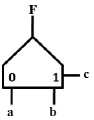
Fig. 1. Logic symbol of 2-1 multiplexer
By conventional method, to realize a function of n variables, the number of modules needed is 2n-1 and the number of levels is n. Any implementation using less than 2n-1 units and n levels is considered as an improvement in the design [9-10].Property of conventional multiplexer (mux) tree is that units in the same level share the same control signal. Due to this there are so many unnecessary transitions/switching of idle multiplexers which involves power loss and heat.
-
II. Related work
In [11], Nan-Shing Li, et-al s uggested a specific controller for selecting appropriate control signals so that unnecessary transitions of unused multiplexers could be avoided. But it is suitable only when the number of input variables is more. This is because some amount of power is needed for the controller too. Power consumed by the controller may be more than the power saved in the mux tree in such cases. In [7] attempt has been made for the evolutionary design of combinational logic circuits with 2-1 mux using Genetic Programming. Even though the number of multiplexers was less compared to standard implementation, the circuits were not optimal.
In ref [10], an exhaustive algorithm was proposed for the design of circuits up to 4 variables using multiplexers, which is not based on evolutionary method. In [12] Cecılia Reis proposed the design of combinational logic circuits based on Genetic Algorithm using minimum number of gates. Some of the circuits implemented were 2-1 multiplexer, 4 bit parity checker etc. The major bottleneck he suggested was the problem of scale and time for convergence. As the number of inputs increases, a large search space is needed. In our previous papers [13-14] evolutionary approach has been made on the design of logic circuits using 2-1 multiplexers up to 4 variables. But in that work no analysis/comparison were made for the power consumption (leakage and dynamic power) and area involved. In [15] evolutionary design of combinational circuits has been done using 2-1 Reed Muller logic blocks, based on 2VROBDD technique.
The problem is to evolve optimal digital circuits using Genetic Algorithm and single control line multiplexers which satisfy specified truth table. It is expected to evolve combinational logic circuits with least possible complexity.
The paper is structured as follows: Section III discusses the formulation of algorithm for the circuit, section IV gives the implementation of logic circuits using the proposed methods, section V deals with the results and comparison with standard implementation technique and section VI gives conclusion.
-
III. Algorithm Formulation
-
A. Representation of chromosome for the circuit
Single output combinational logic circuits specified by the Boolean logic table are considered in this paper. The objective is to implement a fully functional circuit with least possible complexity. Once a 100 % fit circuit is evolved, check for redundancy of units is made and redundant units are eliminated so that the circuit generated is optimal.
Any combinational digital circuit can be realized using a cascade of universal building blocks such as RM ULM (1) or 2-1(single control line) multiplexers. e.g.:, For a 3variable function, there will be 7 units distributed as 4 units in the first level (bottom most level), 2 units in the second level and 1 unit in the top (third) level. Attempt has been made to reduce the number of levels/units. The optimal circuit need not have all the seven units or all the three levels. Chromosomes are encoded so that it gives a functional description of the circuit to be evolved.
In this section, encoding of an individual A (sample circuit) is shown in figure. Individual A is created at random which contains the information about the presence or absence of a unit, corresponding inputs, control signals and outputs as genes. The chromosomes for GA is coded in a one dimensional pattern where each bit or a combination of bits denote a particular input or control signal to the multiplexers. Hence the presence of a unit is identified by 1 and absence by 0 in the chromosome. Fig.2 represents the chromosome used to represent a multiplexer in the first level of implementation (starting from the bottom) of a three variable circuit. Bit X1 is used to check the presence of the multiplexer. If it is zero it means that there is no unit, otherwise it indicates the presence of a unit and bit X2 represents the different input conditions to the multiplexer and X3 and X4 combinations check the control input to the multiplexer. Here if X2=’0’, then the input to the multiplexer is considered as ‘0, 1’ otherwise it is ‘1, 0’. If X3X4=”00” then the control input is taken as ‘a’,”01” is taken as ‘b’ and soon.
X1 X2 X3 X4
Fig. 2. Chromosomal representation of a multiplexer
Similarly the multiplexers for other levels are coded considering the various possibilities of inputs and control signals.
-
B. Selection process and fitness function
A set of individuals (population) is created randomly and fitness for each individual is calculated. Based on the survival of the fittest strategy, fitter individuals are selected to form the new population. Roulette wheel selection technique has been adopted here. Crossover and mutation are applied on the selected members and a new population is created and the process is repeated until the desired condition is met. Fitness of each individual is calculated based on the closeness to the desired truth table.
Fitness function used is
Ν - SUM(XOR(O ! ,O2))
% FITNESS = ( ) × 100
where O 1 is the evolved output, O 2 is the desired output and N is the number of rows in the truth table.
On running the GA, a 100% fit circuit matching exactly with the used defined truth table may be evolved.
Once a 100 % fit circuit is evolved, check for redundancy of units is made and redundant units are eliminated so that the circuit generated is optimal.
-
IV. Proposed Technique
While implementing a Boolean function, sub functions are very useful. To build a hardware circuit for a function with n variables, we have the identities
F= F’(Aj)’ +F’’(Aj) (1)
F = Fʼ(Aj)ʼ xor(FʼʼʼAj) (2)
where Fʼ , Fʼʼ and Fʼʼʼ are functions of n-1 variables.
Equation (1) represents Shannon’s decomposition which is applicable to realization of functions using Multiplexers whereas equation (2) represents Davio decomposition which is valid for realization of functions using Reed Muller units. Both identities help us to reduce the original design problem to two smaller problems. Applying such a decomposition over and over again each time with another variable Aj allows the process of synthesis to be reduced further and further to either literals or constants [15].
Conventional design which is based on Shannon’s decomposition technique permits the use of only same control signals to all the multiplexers in a level and the number of levels needed is equal to the number of variables involved in the function. Two modifications are being proposed so that circuits are evolved with least possible complexity.
-
A. Flexibility in Selecting control input (Modified Method
I)
Here Shannon’s decomposition technique is modified in such a way that the control signal is also generated at random and circuits are evolved using GA. The same variable need not be applied as control signals in a level. The flexibility for the circuit is achieved by coding the chromosomes in such a way that a multiplexer in a particular level can have input from all possible combinations of previous level outputs, 0 or 1 and control input is also made flexible which need not be the same for all the multiplexers in a level. Circuits have been evolved for 2, 3, 4 and 5 variable functions using this technique with lesser number of units and levels, thus reducing the area, power, cost and delay.
Example1. F(a,b) = Σ (1,2,3)
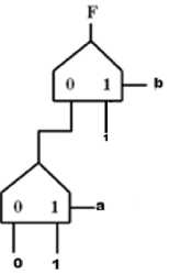
Fig. 3. Circuit evolved for F(a,b) = Σ (1,2,3)
Fig. 3 shows the circuit evolved for a 2 variable function and it can be seen that the circuit needs only 2 units as compared to 3 units with the standard implementation, thereby saving one unit.
Example2. F(a,b,c)=∑(0,4,6,7)
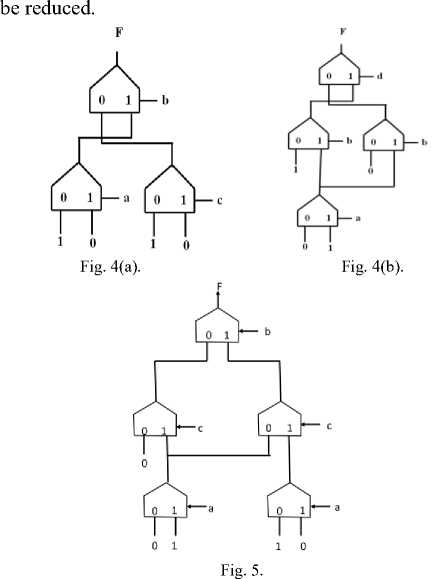
Fig.4(a) shows the optimized circuit evolved for the three variable function F(a,b,c)=∑(0,4,6,7) with the modified method I using GA. It is seen that in the first (bottom) level the control inputs are c and a- not the same variable as in standard method. The function was realized with three multiplexers. Thus with the proposed design, there is a saving of 57% compared to standard implementation.
But with Shannon’s decomposition method using GA the optimal circuit needs 4 units as shown in fig. 4(b). It can be seen that the control signal in a particular level is the same.
Example 3. F(a,b,c) = Σ( 3,5,6)
The circuit generated with the proposed technique as shown in fig.5 has only 5 units, whereas standard implementation procedure needs 7 multiplexers. In [8] with Genetic programming, the synthesis of the same function requires 6 units. On saving the number of multiplexers, cost and power consumption will definitely
Example 4. F(a,b,c,d) = Σ( 0,4,6,7,8,12,14,15)
The evolved circuit has only 4 units without giving flexibility in selecting the control signal, thereby saving 11 numbers as compared to standard implementation as shown in fig. 6(a). But when flexibility is provided in the selection of control signals, the circuit needs only 3 units and 2 levels as shown in fig. 6(b). As the number of levels got reduced, the delay involved will also be reduced by the proposed design.
Example 5. F(a,b,c,d,e) = ∑(0,1,9,22,23,25,30,31)
With standard implementation technique, to implement a five variable function, 31 units are needed with 5 levels. But with the proposed approach, the circuit could be realized using only 10 multiplexers thereby a saving of 21 units is achieved. Fig. 7 shows the circuit evolved for the above function.
F
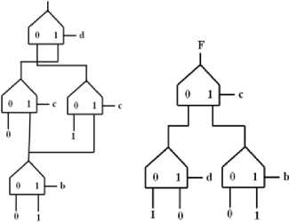
Fig. 6(a). Fig. 6(b).
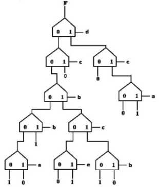
Fig. 7. F(a,b,c,d,e) = ∑(0,1,9,22,23,25,30,31)
-
B. Functions also as control signals(Modified method II)
In the previous method, control inputs of the multiplexers were selected at random from the set of variables of the function. Here a further modification has been made in selecting the control inputs, i.e., a function can also be given as control input instead of variable. Thus control signals can be variables of the function or the outputs of multiplexers in previous level. With this technique, the number of units and number of levels required is again reduced significantly.
For functions up to 4 variables, this method does not guarantee any reduction in the complexity of the circuit than the previous method. But as the number of levels go high, this method produces better results as illustrated by the following example.
F(a,b,c,d,e)= ∑(0,1,9,22,23,25,30,31)
The generated circuit for the above function (fig.8) needs only 9 units and 4 levels, whereas the previous method needs 10 units and 5 levels and the standard implementation needs 31 units and 5 levels. As the number of modules is reduced, the area, cost and power consumption get reduced. As the number of levels got reduced from 5 to 4, the delay involved is also reduced.
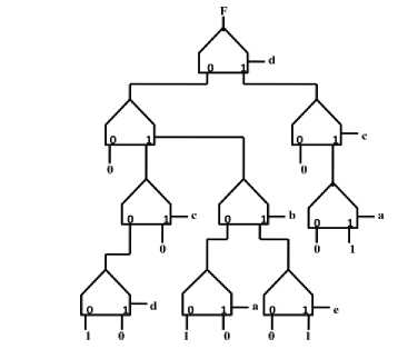
Fig.8. F(a, b, c, d ,e) = ∑(0,1,9,22,23,25,30,31)
-
V. Results
The parameters selected for GA were population size=1000, number of generations=100, crossover rate=0.7, mutation rate=0.3, Roulette wheel selection technique has been used for selecting the individuals for crossover. The simulation was done in MATLAB R2012a. The evolved circuits from GA has been implemented on Spartan 3 Xilinx FPGA using VHDL. Synthesis of the generated circuits was based on CMOS logic family and 90nm technology node using the tool Synopsys Design Compiler.
Functions implemented
> F 1(a,b)=E(1,2,3)
> F2 (a,b,c)=Z(0,4,6,7)
> F3(a,b,c,d)= 2(0,4,6,7,8,12,14,15)
> F4 (a,b,c,d,e) = ^(0,1,9,22,23,25,30,31)
The combinational circuits evolved for the above functions using the proposed methods were analyzed and consolidated.
Table 3 shows the number of levels needed for the evolved circuits and the corresponding delay. For a function of n variables, the circuit needs n levels with the conventional method, but with the proposed methods, it is seen that the number of levels for the generated circuits is reduced. It is obvious that as the number of levels gets reduced, the delay involved is also reduced considerably.
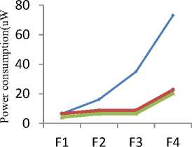
Power consumed in a CMOS VLSI circuit can be classified into 1) Leakage power and 2) dynamic power and on analysis it was found that both leakage and dynamic power has been reduced significantly compared to standard implementation.
Table 4 shows the analysis of power consumption of the circuits by various approaches. On comparing with the traditional method of implementation, for the 5 bit function considered, the % reduction in dynamic and leakage power consumption with the proposed method are 72.41 and 74.9 respectively. The reduction in number of modules will lead to reduced power consumption as is evident from table 4. Both methods perform far better compared to the traditional method.
A simplified Design involves lesser number of units, interconnections and levels. The proposed design meets the qualities of an efficient design such as reduced power consumption, delay and area
Table 1. Comparison in terms of number of units
|
F |
No.of variables |
Standard implementation |
Method1 |
Method II |
||
|
No: of Muxes |
No: of Muxes |
%Saving |
No: of Muxes |
% Saving |
||
|
1 |
2 |
3 |
2 |
33.33 |
2 |
33.33 |
|
2 |
3 |
7 |
3 |
57.14 |
3 |
57.14 |
|
3 |
4 |
15 |
3 |
80 |
3 |
80 |
|
4 |
5 |
31 |
10 |
68.8 |
9 |
71 |
Table. 2. Net Interconnect area in number of units
|
F |
No: of variables |
Interconnect Area and Cell Area in number of units |
||||
|
Standard implementation |
Method1 |
Method II |
||||
|
Total Area |
Total Area |
% Saving |
Total Area |
% Saving |
||
|
1 |
2 |
34.04 |
34.04 |
0 |
22.71 |
33.29 |
|
2 |
3 |
79.39 |
45.38 |
42.84 |
34.04 |
57.12 |
|
3 |
4 |
1 170.276 |
98.58 |
42.10 |
78.918 |
53.65 |
|
4 |
5 |
363.45 |
143.4 |
60.54 |
118.28 |
67.45 |
Table. 3. Delay involved in various methods
|
F |
No: of variables |
Standard Implementation |
Proposed Method (MethodII) |
||
|
No: of levels |
Delay(ns) |
Levels |
Delay(ns) |
||
|
1 |
2 |
2 |
0.25 |
2 |
0.24 |
|
2 |
3 |
3 |
0.37 |
2 |
0.25 |
|
3 |
4 |
4 |
048 |
2 |
0.25 |
|
4 |
5 |
5 |
0.70 |
4 |
0.48 |
Table 4. Comparison in terms of power consumption
|
F |
No: of variables |
Standard Implementation |
Method I |
Method II |
||||||||
|
Dynamic power (uW) |
Leakage power (nW) |
Total power (uW) |
Dynamic power (uW) |
Leakage power (nW) |
Total power (uW) |
% saving |
Dynamic power (uW) |
Leakage power (nW) |
Total Power (uW) |
% saving |
||
|
1 |
2 |
6.3084 |
249.9 |
6.5574 |
6.3084 |
249.9 |
6.5574 |
0 |
3.997 |
166.6 |
4.1636 |
36.5 |
|
2 |
3 |
15.553 |
583.1 |
16.136 |
8.4143 |
333.2 |
8.7463 |
45.79 |
6.308 |
249.9 |
6.553 |
59.39 |
|
3 |
4 |
33.805 |
1 249.5 |
35.01 |
8.4848 |
333.2 |
8.817 |
74.8 |
6.3365 |
249.9 |
6.5855 |
81.19 |
|
4 |
5 |
70.50 |
2582.3 |
73.082 |
22.26 |
416.5 |
22.677 |
68.9 |
19.452 |
648.45 |
20.1 |
72.49 |
Fig.11 shows the power consumed by the evolved circuits by Standard implementation technique and the proposed methods. It is obvious that the power consumption is reduced significantly in the circuits generated by method II.
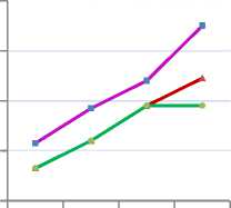
Fig.12 shows the comparison of delay involved for the circuits in the proposed method with the delay in circuits designed by conventional method. It was observed that using the proposed method, the delay for the 5 bit function is 0.48 nsec compared to 0.7 nsec with the conventional method. As the number of bits is increased, the performance of the evolved circuits would be better as the number of levels and the number of units is reduced.
Functions
Fig. 11. Power consumption in various methods
' Std Imp
< :--Method I
^^^^^ Method II
0.8
0.6
0.4
0.2
■ Std Imp
—^*— Method I
^— I— Method II
F2 F3 F4 F5
Functions
Fig. 12. Delay involved in various methods
-
VI. Conclusion
A simplified technique which uses lesser number of units, interconnections and levels has been proposed. This technique uses GA as the optimization tool. Functions up to 5 variables have been implemented and detailed analysis of the evolved circuits for area, power and delay has been made. The results were compared with that of the methods available in the literature. On synthesis, it was found that the circuits evolved by the two new approaches are superior to the design by traditional methods. Method II outperforms standard implementation and method I. Numbers of modules, area, delay and power consumption of the evolved circuits were reduced significantly, which ensures better performance.
References A Simplified Efficient Technique for the Design of Combinational Logic Circuits
- Ahmed T. Soliman and Hazem M. Abbas,” Combinational Circuit Design Using Evolutionary Algorithms”, Electrical and Computer Engineering 2003. IEEE CCECE 2003 Canadian Conference vol.1 pp. 251-254.
- F. Miller and Peter Thomson, “Discovering Novel Digital Circuits using Evolutionary Techniques”, IEE Colloquium on Evolvable Systems, London, 1998.
- Slowik and Michal Bialko,. “Evolutionary Design of combinational Digital Circuits: State of the Art, Main Problems, and future Trends,” Proceedings of the First International Conference on Information Technology 19-21 May 2008,pp.1-6.
- C.K Vijayakumari, P.Mythili, ” A Faster 2 D Technique for the design of combinational digital circuits using Genetic Algorithm”. Proc. of International conference (EPSCICON) 2012, pp. 1-5.
- C. Coello and A. Christianses, ”Use of Evolutionary techniques to automate the design of Combinational Circuits”, International Journal of Smart Engineering System Design 2000, pp. 299-314..
- David E. Goldberg, Genetic Algorithms in Search, Optimization, and Machine Learning. Addison-Wesley, 1989.
- A.H Aguirre and C A Coello Coello, “Using Genetic Programming and multiplexers for the synthesis of Logic Circuits” Proceedings of 2003 NASA/DoD Conference on Evolvable Hardware, 2000, pp. 46-53.
- H Aguirre and C A Coello Coello,Bill P Buckles,”Circuit design using Genetic programming-an illustrative study”,10th NASA Symoposium on VLSI Design 2002.
- C.Coello, A.Christian and A.Aguirre, ”Automated Design of Combinational Logic circuits using Genetic Algorithms,” Proc. of the International Conf on Artificial Neural Nets and Genetic Algorithms “pp. 3335-3338,1997.
- Rekha K. James, Shahana T. K, K. Poulose Jacob,Sreela Sasi, "Delay-Reduced Combinational Logic Synthesis using Multiplexers", Proc .of International Conference on Embedded systems and Applications, pp.105-110.
- Nan-Shing Li, Juinn-Dar Huang, and Han-Jung Huang,“Low Power Multiplexer Tree Design Using Dynamic Propagation Path Control”, IJCSNS International Journal of Computer Science and Network Security, VOL.8 No.9, September 2008, pp.838-841.
- Cecilia Reis, J. A. Tenreiro Machado, and J. Boaventura Cunha,”Evolutionary design of combinational logic circuits”, Journal of Advanced Computational Intelligence and Intelligent Informatics Vol.8 No.5, 2004, pp. 507-512.
- C.K.Vijayakumari, P.Mythil, Rekha.K.James,” An Improved design of Combinational Digital Circuits with Multiplexers using Genetic Algorithm”, IET Proc. of CIIT2013, oct18-19, 2013, pp. 225-229.
- C.K Vijayakumari, Lukose Dileep,P. Mythili, Rekha K. James”, An Improved design of Combinational Digital Circuits with Multiplexers using Genetic Algorithm”, International Conference on Microelectronics, Communication and Renewable Energy(ICMiCR-2013), july2013,India. pp. 2-7
- Khalid Faraj and AE A Almaini, Optimal polarity of Dual Reed Muller expressions",7th WSEAS International Conference on Microelectronics, Nanoelectronics, Optoelectronics (MINO '08), Istanbul, Turkey, May 27-30, 2008ISBN: 978-960-6766-65-7,ISSN: 1790-5117, pp. 45-52.
- A. J. Umbarkar, M S Joshi, P D Sheth, “Dual Population Genetic Algorithm for Solving Constrained Optimization Problems” I.J. Intelligent Systems and Applications, 2015, 02, 34-40 DOI: 10.5815/ijisa.2015.02.05.
