A Study of Graphene

Author: Lakshmy Sukumaran
Journal: International Journal of Education and Management Engineering(IJEME) @ijeme
Article in issue: 1 vol.4, 2014.
Free access
Much debate has been going on as to how nanotechnology will impact the way we live. With the discovery of Graphene, an atom thick allotrope of Carbon, new doors have opened with regard to its potential uses in the field of nanotechnology and possibilities seem endless. Much of the attention is now directed towards achieving a scalable means of production of graphene. The paper tries to highlight the properties of graphene which makes it widely sought after and lists some of the possible applications and uses.
Graphen, Introduction to graphene, Properties of graphene, Applications of graphene
Short address: https://sciup.org/15013824
IDR: 15013824
Text of the scientific article A Study of Graphene
Published Online January 2014 in MECS DOI: 10.5815/ijeme.2014.01.02
-
1. Main text
Much debate has been going on regarding the wide and future implications of nanotechnology. It has the potential to affect every single aspect of our lives and have been considered by many to be the field that might be responsible for the next technical leap in our era. Critiques have also panned it citing its environmental impact, its potential effects on global economy and concerns of toxicity, so much so that there are also doomsday prophecies surrounding it. With the field under immense scrutiny it will be good to assess and analyze the latest advancements in this field. One such would be the discovery of Graphene and its potential impact on variety of areas.
In 2010, two Russian scientists, Andre Greim and Konstantin Novoselov, were given the 2010 Nobel Prize in Physics for their discovery of Graphene. This alone indicates the significance of this discovery and is considered by many to be the rising star in the field of material science and condensed matter physics.
-
1.1. What is Graphene?
Graphene is an atom thick layer of Carbon atoms arranged in a honeycomb lattice. Prior to its isolation in 2004, it was generally believed that two dimensional elements could not exist due to thermal instability. The Carbon to Carbon to bonds in Graphene is so strong that it prevents the thermal fluctuations from destabilizing
* Lakshmy Sukumaran. Tel.:+91 9900724344
it. It is one of the thinnest materials in the world as well as one of the strongest in the world, much stronger than steel and lighter. [1]
-
1.2. Why Graphene?
The answer to this question everyone is asking is its remarkable material properties like ballistic conductance, charge carrier mobilities etc. The properties of graphene are significant in this direction and are discussed in the next section. Standard CMOS technology can be applied to graphene to make much faster devices. Graphene may very well be used as a replacement for indium selenide in solar cells which are relatively more expensive.
Pristine graphene boosts of a lot of amicable properties which are very well suited for new electronic devices and applications. However, defects in graphene along with its dielectric environment and high contact resistance might limit the performance. Another significant point to note is that graphene has no energy gap and hence MOSFETs built of graphene will show am bipolar behavior and cannot be switched off. This may very well be one of the reasons as to why the general interest in the industry is now steered more towards analog RF applications instead of the conventional logic RF applications. Graphene optical properties are supposed to be 100 times faster than conventional switches.
The manufacturing process also is a major issue now as the current processes are either not scalable or practical for mass production. Scotch tape technique, where thinner strips are peeled off, of a block of graphite using a sticky tape is not suitable to make the substance in bulk. Graphene is also an atom thick and thereby whatever you do on that might very well hamper the properties which made it desirable in the first place. Another method in place is the chemical vapor decomposition where the carbon atoms are extracted from a carbon rich source by a process called reduction. But this also suffers from the disadvantage of finding a good substrate for growing the graphene on and also for extracting thin layers without any damage.
Much of the above mentioned drawbacks can be limited to a great extent with strides in technological advancements and Graphene as of now holds the key for the industries to engage in this stride. A lot of promising techniques are now emerging but all these are still in a nascent stage and not yet mature. [2]
-
1.3. Properties of Graphene
Graphene is a single atomic layer of graphite, which is an abundantly found mineral. Graphite is an allotrope of carbon with very tightly bonded carbon atoms organized in the shape of a hexagonal lattice. The sp2 hybridization and thin (0.345Nm) atomic thickness renders very unique properties which are discussed below.
-
• Electronic properties: How electrons flow in a sheet of Graphene, one atom thick is one of the hottest topics being researched now Graphene is a very good conductor. Research have indicated that electrons can transfer through this sheet at speeds reaching one hundredth the speed of light, as if they carry no mass.
-
• Thermal and thermoelectric properties: The structure of Graphene makes it a perfect thermal conductor. The thermal conductivity is seen to be much higher than other carbon nanotubes, diamond and graphite. One more property is that the ballistic thermal conductance is isotropic, meaning it is the same in all directions. This property can have important implications for Graphene based electronic devices. High thermal conductivity is vital in dissipating heat efficiently to keep the devices cool.
-
• Mechanical properties: Graphene is harder than Diamond and is seen to be 300 times harder than steel. Graphene has very high tensile strength and is also very stretchable and robust. This property will have a lot of implications in making a new generation of super strong composite materials. Also special is the fact that coupled with this strong mechanical strength, Graphene also has elastic properties. Tests have shown that Graphene has Spring constant in the order of 1.5 N/m and a Young’s modulus of 0.5 Tpa. The values
-
• Given, however are based on theoretical prospects of using pristine graphene. Properties will deviate from these standard results due to imperfections. However current productions techniques are continuously improving, reducing both costs as well as complexity.
-
• Optical properties: Graphene absorbs around 2.3% of the light that falls on it making it visible to the naked eye. For enhancing visibility these Graphene flakes are usually deposited on silicon wafers. Electrons will act as mass less charge carriers with high mobility. Graphene’s opacity is of the value π
α
-
• ≈ 2.3%. Once optical intensity reaches the threshold which is referred to as the saturation fluence
saturation absorption takes place which means a very high intensity light causes a reduction in absorption. With this property of wavelength independent ultra fast saturation absorption, we are able to achieve full band mode locking.
-
1.4. Summary of properties of Graphene
Table 1: Properties of Graphene
|
Property |
Value |
Comparison with Other Materials |
|
Breaking Strength |
42 Nm-1 |
More than 100 times > steel |
|
Elastic Limit |
-20% |
|
|
Carrier mobility at room temperature |
200,000 cm2V-1S-1 |
More than 100 times > Si |
|
Thenmal conductivity |
-5000Wm-1kK-1 |
More than 100 times > Cu |
|
Maximum current density |
>108 Acm-1 |
More than 100 times > Cu |
|
Optical absorption coefficient |
2.3% |
More than 50 times > GaAs |
-
1.5. Silicon Vs Graphene
-
• Graphene is two dimensional allotrope whereas silicon is single dimensional.
-
• Graphene has 6 electrons whereas Silicon has 14 electrons
-
• Silicon is a pure semiconductor whereas graphene is more like a hybrid between a metal and semiconductor
-
• Density of graphene sheet is > 1g/cm3 whereas silicon has 2.57 g/cm3
-
• Graphene is more lightweight and stronger than Silicon
-
• Break over voltage is < 3v for Graphene whereas for Silicon it is 3 V.
-
• Graphene is zero gap semiconductors which mean that the electron transfer is more than 200 times faster than Silicon.
-
• Graphene has small voltage gain.
-
1.6. Possible Applications
With so much buzz around graphene it is vital that we take a sneak peek at the possible applications and the impact that these can make in the world. The following section sheds light on some of the possible applications of Graphene. [3]
-
• Supercapacitors: A capacitor might be thought of as an energy storage medium and can be considered similar to an electrochemical battery. However comparison should not be made between the potential energy between them and say, fossil fuels. as you will be knowing that most of the commercial and industrial applications relies on fossil fuels.
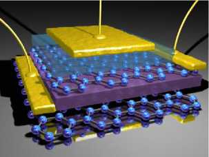
Fig. 1. Supercapacitors
High capacity batteries take a long time to charge whereas capacitors on the other hand charge at a higher rate but releases less energy. The above single cause might be the reason electrically powered vehicles have not yet taken off in the market.
Super capacitors can hold 100 times the amount of electrical charge as standard capacitors. This might even be a possible replacement in many industrial and commercial applications. They also can work under very low temperatures. Super capacitors are already being used in emergency radios and flashlights where energy can be produced kinetically.
A conventional capacitor is generally made of two layers of conductive materials separated by an insulator. The factors that come into play determining the charge it can hold are the distance between the layers and the surface area of the conductors and the dielectric constant of the insulator.
Graphene based capacitors hold a lot of potential as the relative surface area of graphene is extremely high which enables it to hold more charge. Also graphene is significantly lighter. Another notable feature is that as graphene is essentially graphite it is ecologically friendly.
Capacitors as of now can produce up to 150 Farads per gram. The theoretical limit for these Graphene based ultracapactors is placed at 550F/g. Minimal cost of production, lightweight dimensions, elastic and mechanical properties of graphene forms attractive properties for the industry to make use of Graphene in ultracapactors.[4]
-
• Photovoltaic Cells: Graphene offers very low levels of light absorption and very high electron mobility. These properties make it a suitable candidate to replace Si being used now in photovoltaic cells. Si cells are expensive to produce. In case of Si cells, a lot of energy is lost in the form of heat, producing a photon for every electron created when converting light into electricity. Theoretical studies have shown that Graphene on the other hand will absorb these photons and in turn produce multiple electrons. Silicon can only operate on a specific wavelength bands of light whereas Graphene can operate on any wavelengths.
With the above mentioned attractive properties graphene might very well be used to be used as a substitute for Si or gallium arsenide and can find possible applications in graphene based photovoltaic cells that can be used in clothing, mobile phone charging, retro flitted windows and curtains to power your home.
-
• Other Applications
-
• Integrated Circuit
High carrier mobility and low SNR allow it to be used as a channel in FETs.
-
• Anti-Bacterial
Graphene is highly effective for killing E-Coli and can be used in packaging or in hygiene products.
-
• Strength Materials
Since graphene is very strong it can be used as a substitute for Kevlar.
-
• T-Ray Scanners
Detecting hidden objects at security checkpoints and eliminating the risks posed by X-Rays.
-
• Heat dissipation to cool electronics
Overheating in electronic gadgets and laptops is often a hurdle in developing speed and energy efficiency of electronic products. Graphene being a strong hear conductor might help the manufactures.
-
• Efficient dye sensitized solar cells
Conventional dye sensitized solar cells use platinum and graphene can be used as a replacement for platinum. Researchers at Michigan Technological University were able to successfully develop a structure in which graphene sheets were held apart by lithium carbonate. The resulting arrangement was able to convert 7.8 % of conversion of sunlight to electricity.
-
• Electrodes with high surface area and low electrical resistance.
-
• Components with high strength to weight ratios.
-
• Low cost display screens in mobile devices.
-
• Low cost fuel cells.
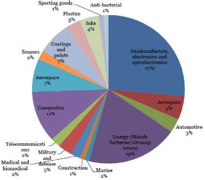
Fig 2: Usage of Graphene
As per the studies conducted, graphene has a wide array of applications, with a major chunk of it in the semiconductor industry. The breakup of the application areas along with their estimated percentages are given in the figure 2.
-
1.7. Alternatives
With so much fuzz and interest surrounding graphene and its possible implications the industry was also gifted with another discovery, Carbyne. The properties of this newly discovered allotrope of carbon boosts properties highly superior than that of Graphene. The only thing limiting the realization of applications listed in the above section is scalability. Modes of production of Graphene as well as Carbyne in a scalable manner are yet to be achieved.
Tensile strength of Carbyne is double that of graphene and is widely heralded as the world’s strongest material. Carbyne is twice as stiff as graphene. Torsional stiffness can also be modified by attaching molecules at the end of the carbon chain.
-
1.8. Conclusion
Graphene was the first two dimensional material to be discovered and many more are being discovered now. Some examples include boron nitride, an atom thick and the best insulator of heat as we now know of, molybdenum disulphide, a three atom thick semiconductor lighter and stronger than silicon. There are around 10 such two dimensional materials which may very well be integrated with graphene to provide extra functionality.
In future, there has been a lot of speculation of electronic displays being integrated and embedded almost anywhere. Many futurists and scientists speculate this as to be the direction where the industry is heading. To achieve this very thin material is required and graphene might very much fit the bill.
Samsung Electronics have successfully demonstrated a single layer of graphene which is around 30 inches in diameter. This is a huge step from the micro meter flakes which we were capable of developing a few years back.
With such a material like graphene which boosts of so many of desirable properties the industry and the general public might be very well poised to develop and see some new applications which might change the way we live.
References A Study of Graphene
- E. M. a. M. Knight, "Graphene: the nano-sized material with a massive future," CNN, 30 April 2013. [Online]. Available: http://edition.cnn.com/2013/04/29/tech/graphene-miracle-material/index.html.
- "Why graphene?," Graphene Update, 2009. [Online]. Available: http://grapheneupdate.com/forum/31-why-graphene.html.
- J. d. L. Fuente, "Graphene Applications & Uses," Sep 21 2013. [Online]. Available:http://www.graphenea.com/pages/graphene-uses-applications.
- J. d. L. Fuente, " Graphene Supercapacitors - What Are They," Sep 21 2013. [Online]. Available: http://www.graphenea.com/pages/ supercapacitors.
