Analysis and Design of Tri-Gate MOSFET with High Dielectrics Gate

Author: Viranjay M. Srivastava, Setu P. Singh
Journal: International Journal of Intelligent Systems and Applications(IJISA) @ijisa
Article in issue: 5 vol.4, 2012.
Free access
The scaling of simple gate transistors requires the scaling and transistor elements like source/drain junction became difficult to scale further after a limit due to adverse effect of electrostatic and short-channel performance. The solution of the problem is tri-gate where we can increase the performance without increasing the width and without scaling. In this paper we have described the parameter of tri-gate and taking the high dielectric as substrate.
Tri-gate MOSFET, Radio frequency, HfO_2, High dielectric constant, CMOS, VLSI
Short address: https://sciup.org/15010251
IDR: 15010251
Text of the scientific article Analysis and Design of Tri-Gate MOSFET with High Dielectrics Gate
Published Online May 2012 in MECS
A tri-gate transistor is an integrated transistor which consists of three gates before going to detailed analysis of tri-gate transistor let us have look the path to tri-gate transistor which covers the journey through double gate. The relationships between charge and potential are different for multi gate transistor and these cannot be mapped with classical junction based transistor hence these follows different modeling [1, 2]. The modeling of tri-gate transistor is quite different. Sallese et. al. [3] had modeled double gate in their publication and the model is valid in all regions of operation, from deep depletion to accumulation and from linear to saturated regimes. Srivastava et. al. [4] has discussed that the double-gate MOSFETs provides good scalability and better immunity to short channel effects, these can overcome the era of CMOS. Sarkar et. al. [5] has developed a model for the noise parameter such as power spectral density and noise figure can be improved with the help of technologies in good extent. The increased electron mobility and velocity at channel surface due to dual gate material reduce effective electrical field at drain end, resulting in smaller DIBL and hot carrier effects [6]. Taur et. al. [7] has presented an explicit continuous models are used for double-gate and surrounding-gate (tri-gate) with no loss of physics. These models inherit all the favorable features from those models, which have been verified. Srivastava et. al [8] have presented a design and performance analysis of cylindrical surrounding double-gate MOSFET which is an advanced version of the Tri-gate, used for the purpose of RF switches.
A tri-gate transistor is an integrated transistor which consist three gates arranged around the three phases of substrate in such a manner that cover the three of four sides (top, side 1, side 2 and bottom). Side 1, side 2, and top are acquired by the gate-1, gate-3, and gate-2 respectively. Gate-3 has physical length L and width W while gate-1 and gate-2 has the length L and width H as shown in the fig. 1.
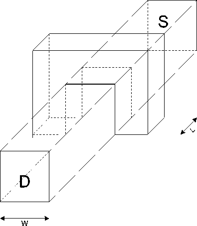
Figure 1. Structure of tri-gate transistor.
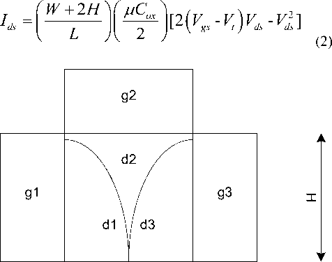
The technology is changing rapidly to keep pace with Moore’s law for that the cell size is reduced more and more scaling of transistors have been done for better packing on chip. But parasitic leakage creates a problem with scaling due to worsening short channel effect. While in tri-gate transistor the short channel effect improved considerably. Tri-gate transistor design utilize low aspect ratio channel to provide evolutionary pathway for CMOS scaling to the end of roadway [9-11]. The design provides the advantages of multi-gate transistor with the advantage of planner MOSFET. TriGate body dimensions are flexible as compared to single gate double and gate transistors and also the plays an important role in determining V-I characteristics [12, 13]. By applying stress memorization techniques we can achieve considerable on-current improvement. As the short channel performance are given by the ratio of W/L. In tri-gate transistor it is given by the ratio of (W+2H)/L. Because the total drives current of the tri-gate transistor is a function of addition of gate-1, gate-2 and gate-3 that is depending on cumulative effect of H, W and H. Hence it is given by (W+2H) over L and not by W over L as in simple transistor. This clearly shows if we increase the height of transistor we will get more drive current.
-
II. M ODELLING OF T RI - GATE MOSFET
The drain to source current in any transistor is proportional to W/L ratio and depends upon the oxide capacitance and the value of the mobility of the majority carriers. In any normal transistor the drain to source current is defined by the equation:
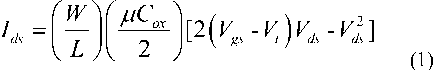
Where Ids is the drain to source is current, Cox is oxide capacitance, µ is mobility of electrons, Vds drain to source voltage, Vgs is gate to source voltage and Vt is threshold voltage of transistor.
The drain to source current in tri-gate transistor is
-
. , W + 2 H . „ . , .„
proportional to ratio. Here H is the width of the transistor and drain to source current is given by the equation:
W
Figure 2. Transverse view of tri-gate transistor.
current characteristics will be improved. Now take the mobility electron in Gallium Arsenide µ = 8500 cm2 V-1s-1 [5], the oxide capacitance C ox = 10.588 nF , then the value of µC ox = 90*10-6 A/V2 , the gate length of transistor is L = .045 μm and height H = 5 μm . Suppose the threshold voltage for transistor V t = 0.6 V and the gate to source voltage V gs = 1 V, 2 V and 3 V, then the equation for the drain to source current for normal gate transistor Ids will be given by the Equation (1) and taking the width of the gate of the transistor W = 22.5 μm .
I ds = 22.5[2(V gs - V V ds — V ds ] = 22.5[0.8V ds - V d, 2 ]
In the above equation we have to put the value of drain to source voltage (Vgs) =1 V .
I ds = 22.5[2( V gs - V t V s - V ds ] = 22.5[2.8V ds - V ds 2 ]
In the above equation we have to put the value of drain to source voltage (V gs ) =2 V .
I ds = 22.5[2(V gs - V t V s - V ds ] = 22.5[4.8 V ds - V ds2 ]
In the above equation we have to put the value of drain to source voltage (V gs ) =3 V .
Now taking another value of width of the gate of the transistor which is higher with respect to the earlier value that is W = 90 μm and calculating the value of drain to source current according to equation (1).
I ds = 90[2( V gs - VV - V d ] = 90[0.8 V - V ds2 ]
In the above equation we have to put the value of drain to source voltage (Vgs) =1 V .
I ds = 90[2( V gs - V)V - V ds ] = 90[2.8Vds - V 2 ]
In the above equation we have to put the value of drain to source voltage (V gs ) =2 V .
I ds = 90[2( V gs - V t )V ds - V d ] = 90[4.8 V ds - V ds 2 ]
In the above equation we have to put the value of drain to source voltage (Vgs) =3 V .
Further we have analyze the value of drain to source current I ds for tri-gate transistor for which the drain to source current will be given by the Equation (2). The only change for tri-gate transistor will be the improvement provided by the height of the gate of transistor that is 2H = 10 μm . We analyzed the results for the same values of parameters which we have chosen for the normal transistor and the width of the gate of the tri-gate transistor W = 22.5 μm .
I ds = 32.5[2(V gs - V , )V ds - V d ] = 32.5[0.8Vds - V ds 2 ]
In the above equation we have to put the value of drain to source voltage (V gs ) =1 V .
I ds = 32.5[2(V gs - Vt)V ds - V d ] = 32.5[2.8Vd s - V ds 2 ]
In the above equation we have to put the value of drain to source voltage (Vgs) =2 V.
I ds = 32.5[2( V gs - Vt)V ds - V d ] = 32.5[4.8 V ds - V ds 2 ]
In the above equation we have to put the value of drain to source voltage (V gs ) = 3 V .
Now taking another value of width of the gate of the transistor which is higher with respect to the earlier
Here the current will be increased because the W/L ratio is improved due to addition of 2H and hence value that is W = 90 μm and calculating the value of drain to source current according to Equation (2).
I ds = 100’ 2 i V' - V t )V ds - П ] = 100[0.8 V ds - V 2 ]
In the above equation we have to put the value of drain to source voltage (V gs ) =1 V .
I ds = 100[2( V s — V)V — Vs ] = 100[2.8 V ds — V s 2 ]
In the above equation we have to put the value of drain to source voltage (Vgs) =2 V .
I ds = 100[2( V s — V ) V ds — V ds ] = 100[4.8 V ds — V ds 2 ]
In the above equation we have to put the value of drain to source voltage (V gs ) =3 V .
-
III. S IMULATION R ESULT OF T RI - GATE MOSFET
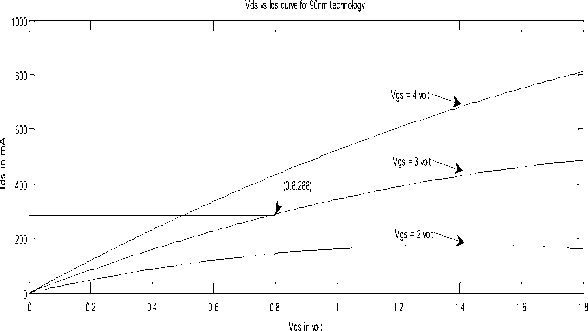
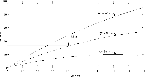
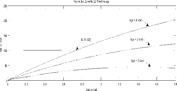
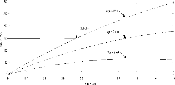
From here we can see that the improvement for small dimensions is considerably greater than large dimensions for larger dimension the drain to source current is 1.1 times of simple gate transistor value but for smaller dimensions the drain to source current is 1.44 times of simple gate transistor value for same width. The simulated MATLAB graphs are shown in the figures.
For smaller dimensions we can see in the graph as in Fig. 4. When the value of drain to source voltage (Vds) is 0.74 V at 4 V gate to source voltage (V gs ) the corresponding values of I ds in simple gate transistors and tri-gate transistors are 100 mA and 144 mA and for larger dimensions when the value of drain to source voltage (V ds ) is 0.8 V at 3 V gate to source voltage (V gs ) the corresponding values of drain to source current (I ds ) in simple gate transistors and tri-gate transistors are 288 mA and 320 mA .
Now let us analyze the tri-gate with another material [14, 15]. We will take the HfO2 for our analysis and will compare it with gallium arsenide. Since the graph of the mobility of electron in HfO 2 ranges from 325 to 375 , so taking the approximated value of the mobility we choose the value 350 . That means µ = 350 and all other parameter and condition will remain same.
After calculating the values of drain to source current (I ds ) for different values of width of the gate (W) for 45 nm technology for all previous values of gate to source voltages (Vds) for tri-gate transistor as well as normal transistor are shown in table 1.
Vds vs Ids curve for simple gate transister
Vds vs Ids curve for Trigate transister
Figure-3 Simulated result for simple and tri-gate transistor the width of gate W = 90 μm .
Vds vs Ids curve for simple gate transister
Vds vs Ids curve for Trigategate transister(corresponding values are 1.4 times of simple gate transister)
Figure 4. Simulated result for simple and tri-gate transistor the width of gate W = 20 μm .
Table 1. Values of I DS (drain to source current) for HfO2
|
Type of transistor |
W(µm) |
V gs (Volt) |
I ds (mA) |
|
Normal |
22.5 |
1 |
0.926[0.8 V ds - V ds 2 ] |
|
2 |
0.926[2.8 V ds - V ds 2 ] |
||
|
3 |
0.926[4.8 V ds - V ds 2 ] |
||
|
90 |
1 |
3.705[0.8 V ds - V ds 2 ] |
|
|
2 |
3.705[2.8 V ds - V ds 2 ] |
||
|
3 |
3.705[4.8 V ds - V ds 2 ] |
||
|
Tri-gate |
22.5 |
1 |
1.338[0.8 V ds - V ds 2 ] |
|
2 |
1.338[2.8 V ds - V ds 2 ] |
||
|
3 |
1.338[4.8 V ds - V ds 2 ] |
||
|
90 |
1 |
4.118[0.8 V ds - V ds 2 ] |
|
|
2 |
4.118[2.8 V ds - V ds 2 ] |
||
|
3 |
4.118[4.8 V ds - V ds 2 ] |
Table-2 Values of I DS (drain to source current) for comparison between GaAs and HfO2.
|
Material |
Type of transistor |
W(µm) |
V gs (Volt) |
I ds (mA) |
|
HfO 2 |
Normal |
22.5 |
1 |
0.926[0.8 V ds - V ds 2 ] |
|
2 |
0.926[2.8 V ds - V ds 2 ] |
|||
|
3 |
0.926[4.8 V ds - V ds 2 ] |
|||
|
90 |
1 |
3.705[0.8 V ds - V ds 2 ] |
||
|
2 |
3.705[2.8 V ds - V ds 2 ] |
|||
|
3 |
3.705[4.8 V ds - V ds 2 ] |
|||
|
Tri-gate |
22.5 |
1 |
1.338[0.8 V ds - V ds 2 ] |
|
|
2 |
1.338[2.8 V ds - V ds 2 ] |
|||
|
3 |
1.338[4.8 V ds - V ds 2 ] |
|||
|
90 |
1 |
4.118[0.8 V ds - V ds 2 ] |
||
|
2 |
4.118[2.8 V ds - V ds 2 ] |
|||
|
3 |
4.118[4.8 V ds - V ds 2 ] |
|||
|
GaAs |
Normal |
22.5 |
1 |
22.5[0.8 V ds - V ds 2 ] |
|
2 |
22.5[2.8 V ds - V ds 2 ] |
|||
|
3 |
22.5[4.8 V ds - V ds 2 ] |
|||
|
90 |
1 |
90[0.8 V ds - V ds 2 ] |
||
|
2 |
90[2.8 V ds - V ds 2 ] |
|||
|
3 |
90[4.8 V ds - V ds 2 ] |
|||
|
Tri-gate |
22.5 |
1 |
32.5[0.8 V ds - V ds 2 ] |
|
|
2 |
32.5[2.8 V ds - V ds 2 ] |
|||
|
3 |
32.5[4.8 V ds - V ds 2 ] |
|||
|
90 |
1 |
100[0.8 V ds - V ds 2 ] |
||
|
2 |
100[2.8 V ds - V ds 2 ] |
|||
|
3 |
100[4.8 V ds - V ds 2 ] |
IV. R ESULTS AND C ONCLUSIONS
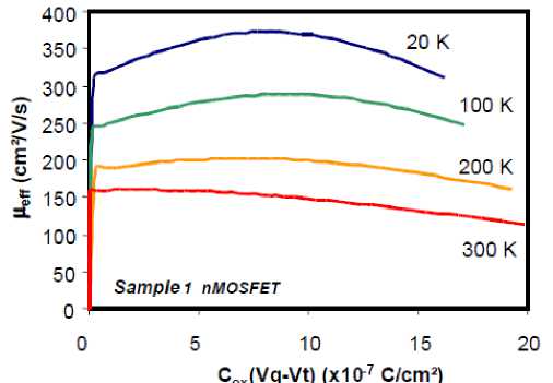
Figure 5. Variation in mobility of electron in HfO 2 with the difference of gate to source voltage and threshold voltage [5].
We have compared the results of Hafnium dioxide and Gallium Arsenide in same condition then we find the only difference in mobility of electrons in the materials. Which affects the result considerably and the Hafnium dioxide has lesser value of mobility hence gives lower value of drain to source current. The table 2 shows the comparison of the values of drain to source current in both the cases Hafnium dioxide as well as Gallium Arsenide.
Now if we compare between tri-gate transistor with simple transistors results then for the value of greater width (W = 90 µm) of the transistor the improvement in tri-gate transistor with respect to normal transistor is just only 1.13 time of the simple transistor’s value but for the smaller width (W = 22.5 µm) of the transistor the improvement in tri-gate transistor with respect to normal transistor is 1.44 time which can be verified buy the table 2 and as well as by the simulation results. From this table, if we consider the case of GaAS with 2 V gate to source voltage (Vgs) of width W = 90 µm then improvement is 1.13 times of normal transistor while it is 1.44 times of the normal values in case of width W = 22.5 µm.
In the proposed tri-gate transistor we achieved a better performance without scaling, as scaling of simple transistors need to scale the oxide and junctions. Scaling became problematic after a certain limit because electrostatics and short channel performance getting worse as the gate length is reduced after a limit. Thus scaling provides limits over it and we cannot scale the dimensions as we desire. Since we have to deal with electrostatics and short channel performance, hence we need a technology which do not apply scaling for improvement and that is done in tri-gate. After analyzing the tri-gate we can use this for the purpose of double-pole four-throw RF switch design [16].
Acknowledgement
The authors would like to thank Prof. G. Singh, Department of Electronics and Communication Engineering, Jaypee University of Information Technology, Solan, India, and Dr. K. S. Yadav, Sr. Scientist, CEERI, Pilani, India for many insightful discussions.
References Analysis and Design of Tri-Gate MOSFET with High Dielectrics Gate
- R. Chau, B. Doyle, J. Kavalieros, D. Barlage, A. Murthy, M. Doczy, R. Arghavani, and S. Datta, “Advanced depleted-substrate transistors: single-gate, double-gate, and tri-gate,” Proc. of Int. Conf. on Solid-State Devices and Materials, Japan, 2002, pp. 68-69.
- J. Kavalieros, B. Doyle, W. Rachmady, M. Radosavljevic, N. Zelick, and R. Chau, “Tri-gate transistor architecture with high-k gate dielectrics, metal gates, and strain engineering,” Prog. of Symp. on VLSI Technology, Digest of Technical Papers, June 2006, pp. 62-63.
- J. M. Sallese, N. Chevillon, B. Iniguez, and F. Pregaldiny, “Charge based modeling of junctionless double-gate field-effect transistors,” IEEE Trans. on Electron Devices, vol. 58, no. 8, pp. 2628-2637, Aug. 2011.
- Viranjay M. Srivastava, K. S. Yadav, and G. Singh, “Design and performance analysis of double-gate MOSFET over single-gate MOSFET for RF switch,” Microelectronics Journal, vol. 42, no. 3, pp. 527-534, March 2011.
- N. Mohan kumar, B. Syamal, J. Shamshudeen, K. Vijayan, R. Saravanakumar, S. Baskaran, K. Bharath, and C. K. Sarkar, “Noise performance of gate engineered double gate MOSFETs for analog and RF applications,” Proc. of Int. Conf. on Electrical and Computer Engineering (ICECE-2010), India, 18-20 Dec. 2010, pp. 586 – 589.
- Electronic archive of new semiconductor materials, characteristics and properties, Loffe Physico technical Institute, Russian Federation, St. Petersburg, 2010.
- Bo Yu , Huaxin Lu, Minjian Liu, and Yuan Taur, “Explicit continuous models for double-gate and surrounding-gate MOSFETs,” IEEE Trans. on Electron Devices, vol. 54, no. 10, pp. 2715-2722, Oct. 2007.
- Viranjay M. Srivastava, K. S. Yadav, and G. Singh, “Design and performance analysis of cylindrical surrounding double-gate MOSFET for RF switch,” Microelectronics Journal, vol. 42, no. 10, pp. 1124-1135, Oct. 2011.
- Xin Sun, Qiang Lu, V. Moroz, H. Takeuchi, G. Gebara, and J. Wetzel, “Tri-gate bulk MOSFET design for CMOS scaling to the end of the roadmap,” IEEE Electron Device Letters, vol. 29, no. 5, pp. 491-493, May 2008.
- F. Lime, and B. Guillaumot, “Investigation of electron and hole mobilities in MOSFETs with TiN/HfO2/SiO2 gate stack,” Proc. of 33rd Int. Conf. on European Solid State Device Research, 16-18 Sept. 2003, pp. 247-250.
- S. Kubicek, J. Chen, A. Ragnarsson, R. J. Carter, V. Kaushik, and K. De Meyer, “Investigation of poly-Si/HfO/sub 2/gate stacks in a self-aligned 70 nm MOS process flow,” Proc. of 33rd Int. Conf. on European Solid-State Device Research, 16-18 Sept. 2003, pp. 251-254.
- B. Doyle, B. Boyanov, S. Datta, M. Doczy, S. Hareland, B. Jin, J. Kavalieros, T. Linton, R. Rios, and R. Chau, “Tri-gate fully-depleted CMOS transistors: fabrication, design and layout,” Proc. of Symp. on VLSI Technology, Digest of Technical Papers, 10-12 June 2003, pp. 133-134.
- M. Saitoh, Y. Nakabayashi, K. Ota, K. Uchida, and T. Numata, “Performance improvement by stress memorization technique in trigate silicon nanowire MOSFETs,” IEEE Electron Device Letters, vol. 33, no. 3, pp. 8-10, Jan. 2012.
- Viranjay M. Srivastava, K. S. Yadav, and G. Singh, “Possibilities of HfO2 for double-pole four-throw double-gate RF CMOS switch,” Proc. of IEEE 2011 Int. Symp. on Microwave, Antenna, Propagation and EMC Technologies for Wireless Communications (MAPE-2011), China, 1-3 Nov. 2011, pp. 309-312.
- N. P. Maity, A. Pandey, S. Chakraborty and M. Roy, “High-k HfO2 Based Metal-Oxide-Semiconductor Devices Using Silicon and Silicon Carbide Semiconductor,” J. of Nano Electronics Physics, vol. 3, no. 1, pp. 947-955, 2011.
- Viranjay M. Srivastava, K. S. Yadav, and G. Singh, “Analysis of double gate CMOS for double-pole four-throw RF switch design at 45-nm technology,” J. of Computational Electronics, vol. 10, no. 1-2, pp. 229-240, June 2011.
