Area-power-temperature aware AND-XOR network synthesis based on shared mixed polarity reed-muller expansion

Author: Apangshu Das, Sambhu Nath Pradhan
Journal: International Journal of Intelligent Systems and Applications @ijisa
Article in issue: 12 vol.10, 2018.
Free access
Modern Integrated circuits (ICs) suffer from excessive power and temperature issues because of embedding a large number of applications on small silicon real estate. Low power technique is introduced to reduce the power. With the reduction of power, area of circuit increases and vice versa. It shows a trade-off nature between them. Increase of area is against the trend of technology scaling which demands small area. Due to small area and high power dissipation, power-density increases. As power-density is directly converging into temperature, it emerges as a challenge in front of the VLSI design engineer to minimize the effect of temperature by reducing power-density. In this work, an attempt has been made to reduce the effect of power-density along with area and power so that AND-XOR based circuit is balanced in terms of area, power, and temperature. AND-XOR based reed-muller (RM) mixed polarity circuit forms are considered in this work. Polarity conversions are made in such a way that possibility of maximum sharing among the sub-function is increased. Genetic algorithm is (a non-exhaustive heuristic algorithm) used to select the polarity of the input variable for maximum sharing. The proposed synthesis approach shows 27.11%, 20.69%, and 32.30% savings in area, power, and power-density respectively than that of reported results. For the validation of the proposed approach, the best solutions are implemented in Cadence digital domain to obtain actual silicon area and power consumption. HotSpot tool is used to get the absolute temperature of the circuit.
Area-power-temperature trade-off, Mixed Polarity Reed-Muller, Polarity conversion, Genetic Algorithm, VLSI, HotSpot
Short address: https://sciup.org/15016551
IDR: 15016551 | DOI: 10.5815/ijisa.2018.12.04
Text of the scientific article Area-power-temperature aware AND-XOR network synthesis based on shared mixed polarity reed-muller expansion
Published Online December 2018 in MECS
Reed-Muller (RM) expanded circuits dominate over the AND-OR based switching network because of its advantages to implement the circuits used in the coding theory, telecommunication, linear system, computer arithmetic circuits, error correction and detection circuits, data encryption and decryption circuits since last two decades [1]. However, implementation of circuits based on AND-XOR has so far not become popular due to the following two main obstacles.
-
• Large area and low speed of XOR gates in comparison to OR gates.
-
• High complexity to optimize ESOP based AND-XOR circuit due to non-canonical nature.
The first obstacle is solved with the development of technologies and the advent of various Field Programmable Gate Arrays (FPGAs) devices like ATMEL FPGA series, AT6000 etc. Now, XOR gates are easily realized in ‘universal modules’ or directly available in programmable devices [2]. Regarding the second obstacle, more recently, researchers paid attention to reduce area and power by minimizing node count and switching activity respectively by employing optimization techniques specifically targeted towards AND-XOR representations in the well-known RM form [3, 4]. It is also well established that AND-XOR circuits are well suited for testability [5] and are easily implemented through FPGAs [6]. Based on applications, AND-XOR based circuits realization can be classified as Fixed Polarity Reed-Muller (FPRM), Mixed Polarity Reed-Muller (MPRM), Pseudo Reed-Muller, Generalized Reed-Muller (GRM), EXOR sum of products (ESOP), Kronecker and pseudo-Kronecker forms [3]. Each of these circuit realizations has its own advantages. The proposed work concentrates on the synthesis of MPRM-based circuit realization, as far as XOR synthesis is concerned. The rest of the paper is organized as follows: Section II illustrates a short survey on related work. Section III demonstrates the motivation and basic terminologies used in Shared Reed-Muller expansion. Section IV presents the Genetic Algorithm formulation based on Thermal-aware Shared Mixed polarity ReedMuller problem. Section V detailed the experimental results and finally, section VI draws the conclusion.
-
II. Related Work
RM expansions are state-of-art decomposition technique used to realize the logic functions. Detailed discussion on two-level AND-XOR network synthesis for node reduction is given in article [7, 8]. In the article [9], authors illustrate that AND-XOR intensive logic network requires fewer product terms than that of AND-OR synthesis. A quasi-minimal algorithm based mixed polarity consistent and inconsistent generalized reedmuller expansion for area reduction is proposed in [10]. Two-level AND-XOR PLA minimization problem using positive and negative polarity selection is dealt by Sasao and proposed several heuristic algorithms in modulo-2 SOPs in [9, 11]. Li et al. proposed MPRM based on Kronecker Functional Decision Diagrams using exhaustive search technique for area minimization in [12]. Switching function realization in AND-XOR form has long been proposed as Reed-Muller expansion in [13]. As time passes, several researchers modified the basic canonical form. The switching function representation in which a variable can have positive as well as negative polarity at the same time throughout the function is known as Mixed Polarity Reed-Muller Form (MPRM) as given by Davio and Deschamps in [14]. MPRM expansion results into fewer numbers of product terms than the original and other forms of Reed-Muller expansions with higher testability. MPRM based heuristic approaches for the area and low power applications have been proposed in [4, 15]. An MPRM realization based on genetic algorithm for polarity selection of the multioutput Boolean function to minimize the area is presented by Almaini et al. in [16, 17]. Improved nearest neighbor (INN) based polarity search using hybrid genetic algorithm is proposed in [18, 19]. Graph-based two-level AND-XOR shared Reed-Muller network synthesis is proposed by Ye and Roy in [20]. Several heuristics have been proposed to study the area and power based on probabilistic method and trade-off analysis is reported for MPRM synthesis in [7, 18-19, 21-23]. However, all the reported work ignores the effect of temperature, which is the prominent factor for damaging most of the circuit nowadays. Physical design engineers paid attention to reduce the temperature but the cooling cost become expensive. The cooling solution of high-performance microprocessors is rising at $ 1-3 or more per watt of power dissipation [24]. So, thermal-aware techniques can be introduced in the higher level of VLSI design (like logic or behavioral level) to improve the power and thermal characteristics of integrated circuits. Few works contributes thermal-aware solutions at logic level [25-27]. The value of temperature is unknown at higher levels of VLSI design but it can be limited by controlling the power-density as explained in given equation [28]:
T chp = T amb + R th [ P total I A oa ]
In equation (1), T chip and T amb are the average chip temperature and ambient temperature respectively. R th is the thermal resistance and that can be calculated by the summative equivalent of the substrate (Si) layer, package and heat sink (cm2 °C/W). Total power dissipation and the chip area are represented by Ptotal and Atotal respectively. Considering ambient temperature and thermal resistance constant in equation (1), we can conclude that chip temperature is directly proportional to power-density of the chip. In this article, we have included power-density as one of the fitness parameters along with area and power of the circuit. Contributions of the article are given bellow:
-
• GA-based approach is proposed to get the suitable
input variable polarity for the realization of thermally optimized SMPRM (Shared Mixed Polarity ReedMuller) function.
-
• Power-density is considered as a representative for temperature and temperature is included along with area and power in fitness function of GA.
-
• Considering the importance of power and area, simultaneous optimization of area, power and temperature is done during mixed polarity reedmuller synthesis.
-
• The proposed approach shows 76.05%, 29.09% and 17.42% improvement in area, power and temperature respectively.
Ctual area (in µm2), power dissipation (in nW) and absolute temperature (oC) are calculated using Cadence and HotSpot tool to validate the algorithmic result.
-
III. Shared Mixed Polarity Reed-Muller Expansion and Motivation
-
A. Shared Reed-Muller Expansion
Any n-input canonical (disjoint cube) Boolean function can be represented as AND-XOR based Exor Sum-Of-Product (ESOP) form with 2n different product terms. The generalized form is shown below:
f ( xY , x 2,....., xn ) = avxn ... x2x t © a2x n.. x2x t © ...
2n f ( x1 ,X 2 ,.....,Xn ) = ®E aiX (2)
i = 1
In equation (2), ai represent the presence or absence of product term and that can be given by a , E{0, 1} . © represents the Exor operation. Based on input variable polarity, the RM expansions are classified into several sub-classes. Any arbitrary Boolean function f ( x 1 ,x 2 ,…..,x n )
can be expanded into different sub-class of RM networks by deriving the Davio expansions [29]. The expansions are given in equation (3):
f (x1,x2, ... ,xn) = xi. fx Фx,. f- — Shannon’ s Exp \ f (xi,x2, ... ,xn) = fx Фxi.(fxl Фfx )--Positive Davio \ (3) f (xi,x2, ... ,xn) = fx, Фx,.(fx, Фfx)--Negative Davio/
Where, fx = f (x,,x2, ... , xi_p1, xi^, xn) and f = f (x,x2, ... , x^,,0, xi+j, x„)are the co-factors ofxi.
Several modified versions of this basic canonical form have been studied based on input variables polarity or Davio expansions. The input variables can appear as positive polarity ( x i ) or negative polarity ( x ) or mixed polarity ( x and x ) at the same time in the expansion, then the function is called mixed polarity reed-muller expansion.
SMPRM expansions are used to represent multi-output Boolean functions as:
f = ( f , , f l , ...., f m - 1 ) : B n ^ B m ,
Where B = { 0, 1 }, and the number of input and number of output variables are represented as ‘ n ’ and ‘ m ’ respectively. The ‘ m ’ different logic functions are decomposed into AND-XOR based SMPRM realization by maintaining a sequence of mixed polarity. After realization of all the output functions the identical terms of the sub-functions are shared among themselves, which are represented as SMPRM. By applying MPRM decomposition iteratively and sharing the identical product terms, we obtain a compact SMPRM structure. Area, power, and power-density estimations are illustrated next.
-
B. Area esimation:
The product terms are taken as area for the SMPRM expansions. By altering the polarity of the input variable in a given function, the MPRM expansions may change and the sharing of product terms also may vary. So, the final structure of SMPRM expansion also gets changed. This is the reason for area minimization in a given multioutput function. Example 1, elaborates the formation of SMPRM expansion of the full-adder circuit and corresponding area computation.
Example 1: In full-adder circuit ‘ a ’, ‘ b ’ and ‘ c ’ are the three inputs added to produce the ‘Sum’ and ‘Carry’ outputs. The truth-table and functions are given by:
Table 1. Truth-table of Full-Adder circuit
|
Input |
Output |
|||
|
x |
y |
z |
sum |
carry |
|
0 |
0 |
0 |
0 |
0 |
|
0 |
0 |
1 |
1 |
0 |
|
0 |
1 |
0 |
1 |
0 |
|
0 |
1 |
1 |
0 |
1 |
|
1 |
0 |
0 |
1 |
0 |
|
1 |
0 |
1 |
0 |
1 |
|
1 |
1 |
0 |
0 |
1 |
|
1 |
1 |
1 |
1 |
1 |
The output functions are represented as:
Sum = ^ m f 1 , 2 , 4 , 7 ) = xyz + xyz + xyz + xyz
Carry = ^ m f 3 , 5 , 6 , 7 ) = xyz + xyz + xyz + xyz
The product terms of sum and carry are in disjoint cube form, so all OR-gates can be replaced by XOR-gates. Therefore, the required functions become:
Sum = xyz Ф xyz Ф xyz Ф xyz
Carry = xyz Ф xyz Ф xyz Ф xyz
Both the output functions can be realized as MPRM based AND-XOR network by applying the positive Davio, negative Davio and Shannon’s expansion as given in equation (3). The positive Davio or negative Davio is accomplished by substituting (x; Ф 1) or (x i Ф 1)
respectively and there will be no change for Shannon’s expansion for the desired variable in a particular term in the sub-function. If we apply, positive Davio in variable ‘x’, negative Davio in variable ‘y’ and Shannon’s expansion in ‘z’. The expansions are given below:
Sum = xyz Ф xyz Ф xyz Ф xyz
= ((x Ф 1)yz) Ф ((x Ф 1)(y Ф 1)z) Ф xyz Ф (x(y Ф 1)z)
-
= xyz Ф yz Ф xyz Ф xz Ф yz Ф z Ф xyz Ф xyz Ф xz
After cancellation of redundant terms ( xyz and xyz ), the required function for sum expression becomes:
Sum = yz Ф xz Ф yz Ф z Ф xz (4)
Similarly, if we decompose the carry expression with the same polarity as considered for sum term, the decomposition becomes:
Carry = xyz © xyz © xyz © xyz
= ((x © 1)(y © 1)z) © xyz © (x(y © 1)z) © (x(y © 1)z)
-
= xyz © yz © xz © z © xyz © xyz © xz © xyz © xz
The redundant terms ( xyz , xz and xyz ) are cancelled and the final expression for carry function becomes:
Carry = yz © z © xyz © xz © xyz (5)
Equations (4) and (5) infer that two product terms ( yz and xz ) can be shared between the sub-function, sum and carry. So, the final expression for sum and carry required six (6) unshared product terms and two (2) shared product terms. The area consumed by the fulladder circuit with given input variable polarity are:
Area SMPRM = PTU + PT S (6)
Here, PTU and PTS are unshared product terms and shared product terms respectively. For example 1, the area occupancy is 8 (product terms).
-
C. Power esimation:
With the development and continuous improvement in CMOS IC technology, the power becomes a major bottleneck for further integration. This reduces the battery life and even leads to pre-mature aging of the circuit components. So, reduction of power is another important criterion. The power consumption of CMOS VLSI circuits can be classified into two major categories: dynamic power and leakage power. Leakage power becomes major contributor below 45nm technology. In this work, we have considered only dynamic power dissipation. The dynamic power can be estimated by equation (7).
P dynamcc = в С^ о / ' ! P CV DD V DD - V ) (7)
i
In equation (7), the switching activity at the load and internal node are represented by βL and βi respectively. The load capacitance and internal capacitance are represented by C L and C i respectively. V DD , V T and f indicate the supply voltage, threshold voltage and frequency of operation respectively. Among these switching activity is the dominating contributor in the power equation and contribution is based on charging and discharging of the internal node and load capacitances. All other parameters are user or manufacturer defined. So, switching activity can be considered as power at logic level.
Let us consider that initial inputs are uncorrelated and statically independent of each other, that is,
Prob input = 0 = Prob input = 1 = 1 .
The output of a logic gate changes only when the present state of the output changes its previous state. Thus, the probability of the output of a gate changing its state is given by:
(Prob ,. x Prob ,) + (Prob . xProb v pr_op=0 pvs_op=1/ v pr_op=1 pvs_op=0/
We have also considered that the probability does not change with time, and then the switching activity of a logic gate can be expressed as:
в = 2 X Prob op = 0 X Prob op = !
Switching activity for ‘ j ’ variable AND term is given by:
P and = 2 X (^) X [1 - (^)]
For ‘ p ’ number of AND-gates the switching activity is given by:
P and _ total = £ 2 X (±) X [1 - d-)] (8)
p 2 2
The expression for switching activity for XOR-gate with ‘ q ’ inputs that gives ‘ r ’ ON-probability is:
P XOR
= 2* —
2 q
r
X - (2 q )
Summation of equation (8) and (9) provides the switching activity estimation of SMPRM expansion.
-
D. Power-density esimation:
At the logic level the value of temperature is unknown. By limiting the power-density, the temperature of a VLSI CMOS circuit can be controlled as given by equation (1). It can be defined as the amount of power drawn per unit area. In this work, the total number of product terms (shared and unshared) in SMPRM expansion represents the area and power is estimated by switching activity, hence, required power-density can be defined by equation (10):
Power - density sMpRM = e S MPRM (10)
AreaSMPRM
3n different polarities of SMPRM expansion include the best and optimal solution. The next task is to find an efficient polarity for input variables of SMPRM expansion. In this work, Genetic algorithm based evolutionary algorithm is used to find that optimal polarity.
-
IV. Shared Mixed Polarity Reed-Muller Expansion based problem Formulation using
Genetic Algorithm
Genetic Algorithm (GA) is a meta-heuristic search algorithm that stochastically exploits within a population of the solution to solve optimization problem [30]. GA, a popular optimization algorithm finds its application from healthcare to general studies [31-33]. In the algorithmic process, each solution in a population is assigned a fitness value and behave analogous manner to natural selection as proposed by Darwin. In this section, shared mixed polarity reed-muller (SMPRM) problem formulation is structured to optimize area, power and temperature (power-density) using GA. GA-based optimization is still a popular method among the researchers because of the following reasons:
-
• The fitness of solution is directly calculated using objective information rather than derived or auxiliary knowledge.
-
• In an extremely large solution space, GA considered as excellent search method.
-
• Non-linear parameters can be easily included in fitness function and local optimum can be derived. That contributes to the robustness of the algorithm.
The genetic formulation involves the careful and efficient choice of chromosome encoding of the input variables (each chromosome represents a possible solution), fitness calculation of each chromosome, save the best chromosomes using elitism mechanism, genetic reproduction involving cross-over and mutation operator; and finally termination criterion. An elaborate description of each step is discussed below.
-
A. Chromosome structure
Chromosome structure for a multi-input and multioutput ( n -input and m -output) Boolean function can be represented by a ternary bit string of length n . Each ternary bit represents the polarity for that input variable. The encoding of ternary value for an input variable within the chromosome can be set based on equation (11):
p j
< P j >=< P n , P n - 1 ,... P 1 >
0 if xk appears in positive form
■ 1 if xk appears in negative form
2 if xk appears in mixed form
An example of a typical chromosome structure is given below:
|
Input variable |
x 6 |
x 5 |
x 4 |
x 3 |
x 2 |
x 1 |
|
polarity |
0 |
1 |
2 |
1 |
0 |
2 |
Fig.1. Chromosome encoding
It is inferred from the equation 11 that if a variable is represented with bit ‘0’, then that variable is expressed as positive polarity and for ‘1’ and ‘2’ variables are expressed as negative and mixed polarity respectively. For a six input Boolean function, the structure of a chromosome may be defined by Fig. 1. The second and sixth bits are represented as ‘0’, that is, input variables (x2 and x6) are expressed in positive polarity. Third and fifth input variables (x3 and x5) are represented with ternary variable ‘1’, that is, those variables are expressed in negative polarity. Whereas, first and fourth bits are ‘2’ means corresponding variables are represented as mixed polarity. We considered population size of 50 to 60 depending on the number of input variables. After the creation of an initial population, the next task is to find out all the objective parameters like area, power, and power-density of an individual chromosome as explained before.
-
B. Fitness measurement
Sustainability of a solution in a population of next generation is defined by its fitness function. A function based on a weighted linear combination of all the estimated value of objective parameters (area, power, and power-density) are used to form the fitness function. Fitness function of a chromosome ‘ c ’ can be determined by equation 12.
area ( c ) power ( c )
cost (c) = w------—---+ w2--------—--- ini _ max_ area ini _ max_ power power - density(c)
3 ini _ max_ power - density
In equation (12), ‘ini_max_area’, ‘ini_max_power’ and ‘ini_max_power-density’ are the maximum area, maximum power and maximum power-density of any chromosome after SMPRM realization of the circuit in the first generation. For a chromosome(c), the area, power and power-density are represented by ‘area (c)’, ‘power (c)’ and ‘power-density (c)’. The weight factor w1, w2 and w3 can be set by the designer with w1+ w2+ w3= 1.
-
C. Elitism (Direct copy)
Elitism is a technique to prevent the degradation of the quality of the next generation. This is done by transferring few best-fitted chromosomes from present generation to next generation [34]. This is done not to lose the best-found solutions in a population. In this proposed approach, 10% chromosomes are directly copied to the next generation and are considered them as ‘best-class’ chromosomes. Elitism ensures that best chromosomes are always maintained between the generations and do not inadvertently get degraded by reproduction (crossover or mutation).
-
D. Genetic Reproduction
Two genetic reproduction method, crossover, and mutation bring variations in the chromosome of the new generations and converge the output solution towards the optimum solution.
Crossover: Proposed GA formulation enables two parent chromosomes to generate two new dissimilar offspring by crossing over two randomly selected crossover points. Parent selection in proposed method is not fully random; it is conditionally biased towards the better fitness chromosomes to obtain a better offspring. 80% of the next generation population is created using two-point crossover process. The selections of parent chromosomes are biased towards the ‘best-class’ of the total population. After fitness calculation, 20% of the best chromosomes are grouped and termed as ‘best-class’ chromosomes.
Parent chromosome for crossover can be selected by choosing a uniform random number between ‘0’ and ‘1’. A chromosome from the ‘best-class’ is selected randomly if the generated random number is greater than ‘0.5’. Otherwise, a chromosome is selected from the entire population. After generating each pair of offspring chromosomes, a check is made with the members of the present population and duplicate chromosomes are eliminated.
ptl
ph
Parent
Chromosome (pi)
Pn
Offspring 0 2 1
Chromosome (oci)^________।
Pn
Parent 2 j
Chromosome (pi)
P.
P12
P22
0 0
о 0
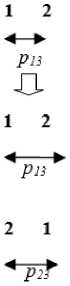
Fig.2. Crossover method 1
and ‘p23’. Using method 1, it produces offspring chromosome ‘oc1’ as ‘p11 (p22) p13’ as shown in Fig. 2. Fig. 3 shows the generation of offspring chromosome using method 2. In this case, offspring chromosome ‘oc2’ is generated as ‘p21 (p12) p23’. After redundancy check, the generated offsprings are contributed as population of next generation.
Mutation: Genetic diversity among the chromosomes can be established by changing few alleles within the offspring using mutation process. The mutation prevents all the chromosomes falling off in the population into a local optimum. 10% of the next generation population is created using mutation process. The operation can be performed by altering few selected random bit positions called mutation points (‘ mp ’) and the polarity of those selected positions are altered by roulette wheel criterion as shown in Fig. 5.
Fig. 4 explains the mutation process. The mutation process is also biased toward the ‘ best-class ’ chromosomes. A random number is generated between ‘ 0 ’ and ‘ 1 ’, if the generated random number is greater than ‘ 0.5 ’ then the parent chromosome for mutation is chosen from ‘ best-class ’ otherwise, from the total population. In Fig. 4, a parent chromosome ‘ x ’ is chosen to participate in mutation operation. Then another random number is chosen between ‘ 1 ’ and ‘ n ’, where ‘n’ is the length of the chromosome to chose the number of alleles for alteration. Let us consider that two (2) numbers of alleles are participating in altering the ternary bit as selected by mutation points ‘ mp 1’and ‘ mp 2’. Alterations of alleles lead to inter-conversion of polarity. Interconversion of polarity is governed by roulette wheel criterion and remaining alleles get unaltered. The newly generated offspring is added to the population of the next generation.
pti
pti
Parent
Chromosome (pi) N—
2 1
1 2
Pn
Offspring 2 12
Chromosome (OC2)<________• pn
Parent 2 12
Chromosome (pi)
P21
P12
P13
0 2
Р-
0 0
P22
Fig.3. Crossover method 2
2 1
P13
2 1
Fig. 2 and 3 show the two methods of generating crossover offspring. Two parent chromosome ‘p1’ and ‘p2’ are selected based on the process explained above, which will generate two offspring chromosomes for next generation. Two arbitrary crossover points ‘pt 1 ’ and ‘pt 2 ’ are selected randomly. Two crossover points, segment the parent chromosomes ‘p1’ and ‘p2’ into three parts. Chromosome ‘p1’ is divided into ‘p11’, ‘p12’ and ‘p13’ whereas; chromosome ‘p2’ is divided into ‘p21’, ‘p22’
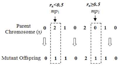
Fig.4. Mutation
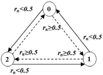
Fig.5. Roulette wheel criterion
The roulette wheel criterion is shown in Fig. 5. A random number ‘ r n’ is generated between ‘ 0 ’ and ‘ 1 ’ for each mutation point. If the generated random number ‘ r n ’ is greater than or equal to ‘ 0.5 ’, the wheel position moves clockwise otherwise, anti-clockwise. Depending on the elevated position, the polarity of the mutation point gets changed.
-
E. Termination Criteria
When there is no improvement in result over the previous 50 generations, the process is suspended and GA is terminated. The best chromosome of last generation is considered as the final solution.
-
V. Experimental Results
In this section, the effectiveness and robustness of the proposed GA-formulation for solving SMPRM problem are presented. The proposed algorithm is coded in LINUX based C-platform and all simulations were carried out on Intel Pentium-IV machine, 3 GHz clock frequency, and 4-GB RAM memory. Proposed optimization method is applied to MCNC and LGSynth93 benchmark suit for experimental validation. 10 independent trail runs are performed to validate the effectiveness of the proposed algorithm for each test case. Complete results are elaborated in 2 sub-sections. The first sub-section elaborates the GA-based algorithmic result concerning the area, power, and power-density of SMPRM and the next sub-section discusses the physical design implementation of the each best and optimum solutions at 45nm technology using CADENCE GENUS and INNOVUS tool. Finally, HotSpot tool is invoked to get the absolute temperature in degree centigrade for each case of the benchmark circuits.
Table 2. Comparison of best solution of proposed approach with respect to AND-OR/XOR [23], SRMDD [25] and MPRM [17]
|
Circuits |
Proposed approach |
AND-OR/XOR [23] |
SRMDD [25] |
MPRM [17] |
Total Execution time (ms) |
||||
|
Area (w 1 =1) |
Power (w 2 =1) |
Pow -Den (w 3 =1) |
Area |
Power |
Area |
Pow-Den |
Area |
||
|
5xp1 |
49 |
5.275 |
0.107 |
61 |
12.29 |
61 |
0.191 |
61 |
1092.88 |
|
9sym |
87 |
3.003 |
0.033 |
- |
- |
- |
- |
- |
1125.21 |
|
alu2 |
257 |
12.748 |
0.038 |
- |
- |
225 |
0.084 |
- |
1037.14 |
|
alu4 |
993 |
20.752 |
0.007 |
- |
- |
- |
- |
2438 |
4336.56 |
|
clip |
118 |
4.568 |
0.038 |
- |
- |
206 |
0.092 |
182 |
709.38 |
|
cm162a |
25 |
5.622 |
0.101 |
25 |
5.48 |
25 |
0.087 |
- |
1351.89 |
|
cm163a |
30 |
5.550 |
0.154 |
18 |
5.09 |
18 |
0.283 |
- |
1378.82 |
|
con1 |
9 |
2.458 |
0.245 |
- |
- |
- |
- |
14 |
849.26 |
|
cu |
21 |
5.049 |
0.140 |
37 |
4.99 |
- |
- |
- |
1077.87 |
|
inc |
34 |
6.556 |
0.139 |
106 |
13.23 |
48 |
0.181 |
34 |
890.08 |
|
misex1 |
19 |
4.534 |
0.156 |
20 |
6.46 |
32 |
0.254 |
13 |
1236.82 |
|
misex2 |
29 |
5.576 |
0.128 |
87 |
9.53 |
- |
- |
- |
251.39 |
|
misex3c |
296 |
38.126 |
0.111 |
- |
- |
- |
- |
1421 |
650.77 |
|
pm1 |
27 |
5.231 |
0.171 |
27 |
6.56 |
- |
- |
- |
170.89 |
|
rd53 |
16 |
4.580 |
0.188 |
20 |
5.61 |
20 |
0.256 |
20 |
801.37 |
|
rd73 |
43 |
7.764 |
0.122 |
- |
- |
64 |
0.211 |
63 |
713.16 |
|
rd84 |
73 |
12.459 |
0.098 |
107 |
20.18 |
- |
- |
107 |
919.41 |
|
sao2 |
74 |
2.884 |
0.034 |
100 |
2.49 |
- |
- |
76 |
1022.36 |
|
table3 |
175 |
13.425 |
0.065 |
- |
- |
- |
- |
401 |
1205.44 |
|
x2 |
18 |
4.652 |
0.136 |
30 |
5.9 |
30 |
0.144 |
- |
1061.10 |
|
Average % overhead w.r.t proposed approach |
-21.13 |
-20.69 |
-14.41 |
-32.30 |
-27.11 |
||||
Table 3. Trade-off analysis with respect to AND-OR/XOR [23], SRMDD [25] and MPRM [17]
|
Weight factor (w 1 , w 2 , w 3 ) |
AND-OR/XOR [23] |
SRMDD [25] |
MPRM [17] |
||
|
Area |
Power |
Area |
Powerdensity |
Area |
|
|
1, 0, 0 |
21.13 |
-9.86 |
14.41 |
-35.94 |
27.11 |
|
0.5, 0.5, 0 |
17.53 |
-4.28 |
11.89 |
-20.83 |
20.65 |
|
0, 1, 0 |
-0.09 |
20.69 |
-2.59 |
13.78 |
11.35 |
|
0, 0.5, 0.5 |
-11.17 |
7.42 |
-15.94 |
20.71 |
-7.21 |
|
0, 0, 1 |
-31.09 |
9.51 |
-40.87 |
32.25 |
-21.49 |
|
0.5, 0, 0.5 |
-3.16 |
0.00 |
-8.42 |
3.02 |
-5.16 |
|
0.5, 0.25, 0.25 |
8.93 |
4.27 |
1.20 |
-2.64 |
9.08 |
|
0.25, 0.5, 0.25 |
-5.51 |
11.84 |
-9.78 |
19.28 |
-1.08 |
|
0.25, 0.25, 0.5 |
-22.36 |
11.24 |
-22.38 |
24.76 |
-13.17 |
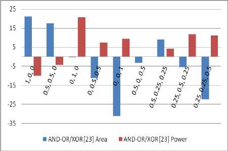
Fig.6. Average percentage improvement of proposed approach w.r.t AND-OR/XOR [23]
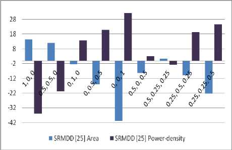
Fig.7. Average percentage improvement of proposed approach w.r.t SRMDD [25]
-
A. Result based on area, power and power-density aware SMPRM AND-XOR network synthesis
In this sub-section, we present the algorithmic result obtained by applying the GA-based algorithm for SMPRM AND-XOR network synthesis. Table 2, reports a comparative study of the best area (w1), best power (w2) and best power-density (w3=1) result of proposed SMPRM AND-XOR network with AND-OR/XOR based fixed polarity decomposition [23], shared reed-muller decision diagram based decomposition [25] and mixed polarity reed-muller decomposition [17]. When 100% weight is given to the area, it is observed that 21.13%, 14.41%, and 27.11% average saving is possible with respect to AND-OR/XOR, SRMDD and MPRM based decomposition respectively. When complete weight is given to power, it is observed that 20.69% power saving is possible with respect to AND-OR/XOR based decomposition. If the decomposition of proposed approach is based on power-density, the power-density is improved by 32.30% with respect to SRMDD based decomposition. By varying the weight factor w1 (associate with the area), w2 (associate with power), w3 (associate with power-density) in a range of 0 to 1 the results are analysed and reported in Table 2. A clear view of trade-off is observed among the area, power, and power-density in Table 2. With the increase of area weight factor, the value of area result is improved but the value of power and power-density is degraded and vice-versa. For trade-off analysis, we have reported results for w1, w2 and w3 for (1, 0, 0), (0.5, 0.5, 0), (0, 1, 0), (0, 0.5, 0.5), (0, 0, 1), (0.5, 0, 0.5), (0.5, 0.25, 0.25), (0.25, 0.5, 0.25), (0.25, 0.25, 0.5) combinations. When the result for these weight factor combinations are compared with AND-OR/XOR based decomposition, it is observed that maximum 21.13% savings in the area for (w1=1, w2=0, w3=0) combination and maximum 11.84% power savings are observed for the combination (w1=0.25, w2=0.5, w3=0.25). When the result of SRMDD based decomposition is compared with proposed approach, it is observed that 14.41% saving in area and 32.25% saving in power-density are achieved for the weight combination of (1, 0, 0) and (0, 0, 1) respectively.
Fig. 6 and 7 show the average percentage improvement of proposed approach with AND-OR/XOR and SRMDD for area, power and area, power-density respectively. It is observed from Fig. 6, Fig. 7 and Table 2 that an optimum solution is obtained for the combination (w1=0.5, w2=0.25, w3=0.25), where 8.93% and 4.27% improvement in area and power is observed with respect to AND-OR/XOR based decomposition respectively. With respect to SRMDD the proposed approach shows 1.20% improvement in the area with an overhead of 2.64% powerThe optimum solution shows area improvement of 9.08% with respect to MPRM based decomposition. In Table 2, ‘-‘ indicates that the corresponding value is not available in the literature. Table 3, reports the trade-off analysis of proposed approach with the AND-OR-XOR and SRMDD based decomposition.
In next section, we are going to discuss physical design implementation of the best result with respect to each objective function and optimum solution. For this,
Cadence Genus and Innovus tools are used to get actual silicon area and power dissipation respectively and HotSpot tool is used to calculate the absolute temperature.
Table 4. Post Layout area, power and temperature comparison of proposed approach with SRMDD based circuit synthesis
|
Circuits |
Proposed approach |
SRMDD[25] |
CPU Time (s) |
||||||||
|
Best solutions |
Optimum solution |
Best solutions |
Optimum solution |
||||||||
|
Area Best (µm2) |
Power Best (nW) |
Peak Temp Best ( OC) |
Area (µm2) |
Power (nW) |
Peak Temp ( OC) |
Area (µm2) |
Peak Temp ( OC) |
Area (µm2) |
Peak Temp ( OC) |
||
|
5xp1 |
140.22 |
1260.02 |
65.36 |
140.22 |
1260.02 |
65.36 |
559.88 |
76.70 |
559.88 |
82.12 |
0.76 |
|
9sym |
54.04 |
1121.23 |
68.15 |
90.28 |
1136.20 |
68.95 |
- |
- |
- |
- |
0.57 |
|
alu2 |
253.42 |
2484.83 |
66.70 |
380.30 |
2610.14 |
68.21 |
2583.16 |
64.05 |
2583.16 |
72.57 |
0.60 |
|
alu4 |
521.89 |
2034.90 |
67.12 |
630.99 |
4299.21 |
69.30 |
- |
- |
- |
- |
0.92 |
|
clip |
176.81 |
1358.89 |
68.20 |
176.47 |
1358.89 |
68.20 |
229.73 |
77.86 |
229.73 |
77.86 |
0.58 |
|
cm162a |
52.32 |
371.48 |
65.41 |
56.77 |
407.94 |
66.50 |
119.75 |
74.63 |
143.04 |
82.65 |
0.42 |
|
cm163a |
35.91 |
187.69 |
63.05 |
41.04 |
210.27 |
63.85 |
169.65 |
73.98 |
179.83 |
78.91 |
0.41 |
|
con1 |
14.36 |
173.46 |
65.87 |
17.10 |
215.59 |
66.07 |
- |
- |
- |
- |
0.38 |
|
cu |
24.40 |
207.31 |
63.89 |
28.12 |
259.90 |
64.82 |
- |
- |
- |
- |
0.35 |
|
inc |
94.73 |
797.85 |
63.80 |
104.65 |
938.22 |
65.75 |
543.04 |
67.93 |
559.81 |
80.44 |
0.63 |
|
misex1 |
39.67 |
303.06 |
63.54 |
42.06 |
320.95 |
63.94 |
239.71 |
73.02 |
276.51 |
77.66 |
0.40 |
|
misex2 |
49.68 |
354.40 |
63.20 |
65.41 |
399.20 |
63.20 |
- |
- |
- |
- |
0.44 |
|
misex3c |
290.21 |
1557.40 |
66.50 |
315.38 |
1730.10 |
67.05 |
- |
- |
- |
- |
0.70 |
|
pm1 |
15.09 |
182.05 |
62.33 |
21.13 |
213.46 |
62.70 |
- |
- |
- |
- |
0.36 |
|
rd53 |
21.02 |
328.58 |
65.92 |
24.96 |
394.14 |
66.87 |
149.87 |
84.90 |
149.87 |
89.32 |
0.40 |
|
rd73 |
40.96 |
598.21 |
68.96 |
46.12 |
716.22 |
68.96 |
446.57 |
78.41 |
446.57 |
78.41 |
0.58 |
|
rd84 |
57.45 |
731.74 |
68.71 |
70.45 |
1003.03 |
69.42 |
- |
- |
- |
- |
0.60 |
|
sao2 |
96.30 |
963.07 |
65.48 |
98.49 |
963.07 |
67.74 |
- |
- |
- |
- |
0.66 |
|
table3 |
728.12 |
2343.71 |
66.07 |
771.55 |
2390.37 |
67.40 |
- |
- |
- |
- |
0.98 |
|
x2 |
27.70 |
170.46 |
62.27 |
32.83 |
214.61 |
64.02 |
166.53 |
96.57 |
166.53 |
73.42 |
0.45 |
|
Average % savings w.r.t. SRMDD best solutions |
74.95 |
- |
13.92 |
72.83 |
- |
12.79 |
|||||
|
Average % savings w.r.t. SRMDD optimum solutions |
76.05 |
- |
17.42 |
74.03 |
- |
16.34 |
|||||
-
B. Physical design implementation at 45nm technology
Algorithmic results presented in section A, depict only representative values for area, power, and temperature. To validate the results obtained from the algorithm, the best and optimum solutions are implemented in physical design domain to obtain the real world values for the area in micrometer, power in nano-watt and temperature in degree centigrade. The solutions are first synthesized using Cadence Genus tool and synthesized solutions are fed into Cadence Innovus tool for obtaining actual silicon area utilization and power dissipation. The floorplan information (.flp) profile is created using silicon area utilization and power profile (.pptrace) is created from power dissipation information. These two files are taken as input to the HotSpot tool [35] to obtain the temperature profile. The total area from floorplan information, power dissipation from power profile and peak temperature in degree centigrade from temperature profile are reported in Table 4 for each benchmark circuit. The ambient temperature at HotSpot is considered as 45.19 °C. The other constraint in HotSpot tool configurations are as follows:
Chip thickness = 0.15mm,
Convection capacitance = 140.4 J/K),
Convection resistance = 5 K/W,
Heat sink side = 60mm,
Heat sink thickness = 6.9mm,
Spreader side = 30mm,
Spreader thickness = 1mm,
Chip to spreader interface thickness = 0.020mm, Dynamic temperature management = above 85 °C.
Table 4 reports the area result of best area solution, power result of best power solution and the peak temperature of the best power-density aware solution of algorithmic solutions mentioned in previous sub section. The weight factor w1=0.5, w2=0.25 and w3=0.25 is considered as the optimum solution at the algorithmic result and that is reported in Table 3. The results are compared with SRMDD and original circuit based on AND-OR decomposition based solutions. It is observed in Table 4 and Table 5 that proposed best area solution shows 74.95%, 76.06% and 1.90% average savings than that of SRMDD best solutions, SRMDD optimum solutions and AND-OR based decompositions respectively. In the case of best power aware solution, the proposed approach shows 29.09% savings with respect to AND-OR based decompositions. When the optimum solution is considered, the area shows an improvement of
72.83% and 74.03% than that of best and optimum SRMDD based decompositions but shows an area overhead of 13.75% when compared with AND-OR based decomposition. Proposed power-aware solution shows an improvement of 19.76% than that of AND-OR based decompositions. When peak temperature is concern, the best temperature aware solutions save 13.92%, 17.42% and 5.07% peak temperature with respect to SRMDD best, SRMDD optimum and AND-OR based decomposition respectively. The optimum solution saves 12.79%, 16.34% and 3.78% average peak temperature with respect to SRMDD best, SRMDD optimum and AND-OR based decomposition. Maximum 18.98 °C (for ‘ rd53 ’ benchmark) and 10.04 °C (for ‘ rd84 ’ benchmark) peak temperature reduction is observed by proposed approach than that of SRMDD best and AND-OR based decomposition. The last column shows the maximum time required to implement a benchmark circuit in Cadence tool in an identical environment. ‘-‘ in Table 4 and Table 5 indicates that the corresponding value is not available in the literature.
Table 5. Post Layout area, power and temperature comparison of proposed approach with AND-OR based circuit synthesis
|
Circuits |
Proposed approach |
AND-OR |
|||||||
|
Best solutions |
Optimum solution |
Un-Optimized Original circuits |
|||||||
|
Area Best (µm2) |
Power Best (nW) |
Peak Temp Best ( OC) |
Area (µm2) |
Power (nW) |
Peak Temp ( OC) |
Area (µm2) |
Power (nW) |
Peak Temp ( OC) |
|
|
5xp1 |
140.22 |
1260.02 |
65.36 |
140.22 |
1260.02 |
65.36 |
77.29 |
1158.53 |
69.49 |
|
9sym |
54.04 |
1121.23 |
68.15 |
90.28 |
1136.20 |
68.95 |
54.04 |
1121.23 |
75.90 |
|
alu2 |
253.42 |
2484.83 |
66.70 |
380.30 |
2610.14 |
68.21 |
295.15 |
2714.74 |
67.44 |
|
alu4 |
521.89 |
2034.90 |
67.12 |
630.99 |
4299.21 |
69.30 |
799.25 |
8194.88 |
73.33 |
|
clip |
176.81 |
1358.89 |
68.20 |
176.47 |
1358.89 |
68.20 |
100.21 |
1405.20 |
71.35 |
|
cm162a |
52.32 |
371.48 |
65.41 |
56.77 |
407.94 |
66.50 |
28.04 |
389.73 |
66.54 |
|
cm163a |
35.91 |
187.69 |
63.05 |
41.04 |
210.27 |
63.85 |
25.99 |
384.68 |
66.57 |
|
con1 |
14.36 |
173.46 |
65.87 |
17.10 |
215.59 |
66.07 |
14.37 |
215.59 |
66.67 |
|
cu |
24.40 |
207.31 |
63.89 |
28.12 |
259.90 |
64.82 |
36.25 |
259.45 |
64.11 |
|
inc |
94.73 |
797.85 |
63.80 |
104.65 |
938.22 |
65.75 |
94.73 |
1037.06 |
67.34 |
|
misex1 |
39.67 |
303.06 |
63.54 |
42.06 |
320.95 |
63.94 |
45.14 |
515.53 |
65.90 |
|
misex2 |
49.68 |
354.40 |
63.20 |
65.41 |
399.20 |
63.20 |
71.82 |
432.52 |
62.66 |
|
misex3c |
290.21 |
1557.40 |
66.50 |
315.38 |
1730.10 |
67.05 |
426.47 |
4389.99 |
71.50 |
|
pm1 |
15.09 |
182.05 |
62.33 |
21.13 |
213.46 |
62.70 |
30.78 |
268.71 |
63.64 |
|
rd53 |
21.02 |
328.58 |
65.92 |
24.96 |
394.14 |
66.87 |
30.09 |
570.23 |
72.15 |
|
rd73 |
40.96 |
598.21 |
68.96 |
46.12 |
716.22 |
68.96 |
58.14 |
1079.04 |
75.76 |
|
rd84 |
57.45 |
731.74 |
68.71 |
70.45 |
1003.03 |
69.42 |
82.76 |
1516.76 |
78.75 |
|
sao2 |
96.30 |
963.07 |
65.48 |
98.49 |
963.07 |
67.74 |
106.36 |
1150.81 |
68.58 |
|
table3 |
728.12 |
2343.71 |
66.07 |
771.55 |
2390.37 |
67.40 |
725.72 |
3099.81 |
69.27 |
|
x2 |
27.70 |
170.46 |
62.27 |
32.83 |
214.61 |
64.02 |
32.15 |
337.74 |
66.42 |
|
Average % savings w.r.t. Un-Optimized AND-OR Circuits |
1.90 |
29.09 |
5.07 |
-13.75 |
19.76 |
3.78 |
|||
-
VI. Conclution
Proposed approach presents a GA-based input variable polarity selection for AND-XOR Shared Mixed Polarity Reed-Muller circuit decomposition. Initially, Area, power, and temperature (power-density) are considered simultaneously as objective parameters. Best and optimum solutions generated at algorithmic process are carried into physical design domain using Cadence Genus and Innovus tools. Finally, HotSpot tool is utilized to generate the temperature profile in degree centigrade. Maximum 76.05% saving in the area, 29.09% saving in power and 17.42% saving in peak temperature are observed using proposed SMPRM-based approach with respect to reported literature. Proposed method establishes that temperature can be controlled by controlling power-density of a circuit at logic level.
Acknowledgment
This work was supported by SMDP-C2SD project sponsored by Deity, Govt. of India.
References Area-power-temperature aware AND-XOR network synthesis based on shared mixed polarity reed-muller expansion
- J. Saul, “Logic Synthesis for Arithmetic Circuits using the Reed-Muller Representation”, IEEE Proceedings of 3rd European Conference on Design Automation. March, 1992. 109-113. doi: 10.1109/EDAC.1992.205904.
- L. Wang, “Automated Synthesis and Optimization of Multilevel Logic Circuits”, Doctoral dissertation, Napier University, 2000.
- T. Sasao, “Switching Theory for Logic Synthesis”, Springer Science & Business Media, 2012.
- W. Pengjun and L. Hui, “Low Power Mapping for AND/XOR Circuits and its Application in Searching the Best Mixed-Polarity”, Journal of Semiconductors, Vol. 32, no.2, 025007, 2011.
- H. Rahaman, D. K. Das and B. B. Bhattacharya, “Testable Design of AND–EXOR Logic Networks with Universal Test Sets”, Computers & Electrical Engineering, Vol. 35, no. 5, pp. 644-658, 2009. doi: https://doi.org/10.1016/j.compeleceng.2009.01.006.
- S. B. Ko and J. C. Lo. "Efficient Realization of Parity Prediction Functions in FPGAs", Journal of Electronic Testing, Vol. 20, no. 5, pp. 489-499, 2004. doi: 10.1023/B:JETT.0000042513.15382.e7.
- S. N. Pradhan and S. Chattopadhyay. “Two-level AND XOR Networks Synthesis with Area-Power Trade-off”, Int. J. Comput. Sci. Network Security, vol. 8, no. 9, pp. 365-375, 2008.
- S. Chattopadhyay, S. Roy, and P. P. Chaudhuri. “Synthesis of Highly Testable Fixed Polarity AND-XOR Canonical Networks - a Genetic Algorithm Based Approach”, IEEE Trans. on Computers, vol. 45, no. 4, pp. 487-490, April 1996. doi: 10.1109/12.494107.
- T. Sasao and P. Besslich. “On the Complexity of Mod-2-Sum PLAs”, IEEE Trans.on Computers, vol. 39, no. 2, pp. 262-266, February, 1990. doi: 10.1109/12.45212.
- M. A. Perkowski, L. Csanky, A. Sarabi and I. Schafer. "Fast Minimization of Mixed-Polarity AND/XOR Canonical Networks", Computer Design: VLSI in Computers and Processors, 1992. ICCD'92. Proceedings, IEEE 1992 International Conference on. IEEE, 1992, pp. 33-36. doi: 10.1109/ICCD.1992.276211.
- T. Sasao. “EXMIN2: A Simplification Algorithm for Exclusive-OR-Sum-of-Products Expressions for Multiple Valued Input Two-Valued Output Functions”, IEEE Transaction on CAD, vol. 12, no. 5, pp. 621-632, May, 1993. doi: 10.1109/43.277608.
- H. Li, P. Wang and J. Dai, "Area Minimization of MPRM Circuits", ASICON'09. 8th IEEE International Conference on ASIC. pp. 521-524, 2009. doi: 10.1109/ASICON.2009.5351633.
- I. Reed. “A Class of Multiple-Error-Correcting Codes and the Decoding Scheme”, Transactions of the IRE Professional Group on Information Theory, Vol. 4, no. 4, pp. 38-49, 1954. doi: 10.1109/TIT.1954.1057465.
- M. Davio, Y. Deschamps and A. Thayse. Discrete and switching Functions. George and McGraw-Hill, NY, 1978.
- H. Wu, M. A. Perkowski, X. Zeng, and N. Zhuang. "Generalized Partially-Mixed-Polarity Reed-Muller Expansion and its Fast Computation", IEEE transactions on computers Vol. 45, no. 9, pp. 1084-1088, 1996. doi: 10.1109/12.537134.
- M. Yang, H. Xu, and A. E. A. Almaini. "Optimization of Mixed Polarity Reed-Muller Functions Using Genetic Algorithm", Computer Research and Development (ICCRD), 2011 3rd International Conference on. Vol. 3. IEEE, 2011. doi: 10.1109/ICCRD.2011.5764198.
- Al Jassani, B. A., N. Urquhart, and A. E. A. Almaini. "Manipulation and Optimisation Techniques for Boolean Logic", IET Computers & Digital Techniques, Vol. 4, no. 3, pp. 227-239, 2010. doi: 10.1049/iet-cdt.2009.0007.
- L. Xiao, et.al., “Optimization of Best Polarity Searching for Mixed Polarity Reed-Muller Logic Circuit”, 28th IEEE International Conference on System-on-Chip (SOCC), 2015, pp. 275-280.
- He, Zhenxue, et.al., "An Efficient and Fast Polarity Optimization Approach for Mixed Polarity Reed-Muller Logic Circuits", Frontiers of Computer Science, Vol. 11, no. 4, pp. 728-742, 2017.
- Y. Ye and K. Roy. "A Graph-Based Synthesis Algorithm for AND/XOR Networks", Proceedings of the 34th Design Automation Conference, Anaheim, CA, USA, 1997, pp.107-112. doi: 10.1109/DAC.1997.597126.
- He. Zhen-Xue, et al., "A Power and Area Optimization Approach of Mixed Polarity Reed-Muller Expression for Incompletely Specified Boolean Functions", Journal of Computer Science and Technology, Vol. 32, no. 2, pp. 297-311, 2017. doi: DOI 10.1007/s11390-017-1723-1.
- X. Wang, et al., "Power Optimization in Logic Synthesis for Mixed Polarity Reed-Muller Logic Circuits", The Computer Journal, Vol. 58, no. 6, pp. 1306-1313, 2015.
- S. Chaudhury, and S. Chattopadhyay, "Fixed polarity Reed-Muller Network Synthesis and its Application in AND-OR/XOR-Based Circuit Realization with Area-Power trade-off", IETE Journal of Research, Vol. 54, no. 5, pp. 353-363, 2008. Doi: http://dx.doi.org/10.4103/0377-2063.48540.
- S. Gunther, F. Binns, D. M. Carmean, and J. C. Hall, “Managing the Impact of Increasing Microprocessor Power Consumption”, Intel Technology Journal, vol. 5, no. 1, pp. 1-9, 2001.
- A. Das, and S. N. Pradhan, “Shared Reed-Muller Decision Diagram Based Thermal-Aware AND-XOR Decomposition of Logic Circuits”, VLSI Design, Vol. 2016, pp. 1-14, 2016. doi: http://dx.doi.org/10.1155/2016/3191286.
- A. Das and S. N. Pradhan, "Thermal Aware FPRM Based AND-XOR Network Synthesis of Logic Circuits," 2015 IEEE 2nd International Conference on Recent Trends in Information Systems (ReTIS), Kolkata, 2015, pp. 497-502. doi: 10.1109/ReTIS.2015.7232930.
- A. Das and S. N. Pradhan, "Thermal aware Output Polarity Selection of Programmable Logic Arrays", International Conference on Electronic Design, Computer Networks & Automated Verification (EDCAV), Shillong, 2015, pp.68-71. doi: 10.1109/EDCAV.2015.7060541.
- M. Pedram and S. Nazarian, "Thermal Modeling, Analysis, and Management in VLSI Circuits: Principles and Methods", in Proceedings of the IEEE, vol. 94 (8), pp. 1487-1501, Aug. 2006. doi: 10.1109/JPROC.2006.879797.
- M. Davio, Y. Deschamps, and A. Thayse, “Discrete and switching Functions”, George and McGraw-Hill, NY, 1978.
- C.K. Vijayakumari, P. Mythili, K. J. Rekha,"A Simplified Efficient Technique for the Design of Combinational Logic Circuits", International Journal of Intelligent Systems and Applications (IJISA), vol.7, no.9, pp.42-48, 2015. DOI: 10.5815/ijisa.2015.09.06.
- S. Goyal, J. Singh, "Two-Level Alloyed Branch Predictor based on Genetic Algorithm for Deep Pipelining Processors", International Journal of Modern Education and Computer Science(IJMECS), Vol.9, No.5, pp. 27-33, 2017.DOI: 10.5815/ijmecs.2017.05.04.
- H. M. Mousa, "DNA-Genetic Encryption Technique", International Journal of Computer Network and Information Security(IJCNIS), Vol. 8, No. 7, pp. 1-9, 2016. DOI: 10.5815/ijcnis.2016.07.01.
- A. Chandel, M. Sood, "A Genetic Approach Based Solution for Seat Allocation during Counseling for Engineering Courses", International Journal of Information Engineering and Electronic Business(IJIEEB), Vol. 8. No. 1, pp. 29-36, 2016. DOI: 10.5815/ijieeb.2016.01.04.
- A. Das, S. R. Choudhury, B. K. Kumar and S. N. Pradhan, "An Elitist Area-Power Density Trade-off in VLSI Floorplan Using Genetic Algorithm", 7th International Conference on Electrical and Computer Engineering, Dhaka, 2012, pp. 729-732. doi: 10.1109/ICECE.2012.6471654.
- HotSpot tool available on: http://lava.cs.virginia.edu/HotSpot/download_form2.html. Accessed: 3rd of July 2017.
