AWG Based Optical Packet Switch Architecture

Author: Pallavi S, M. Lakshmi
Journal: International Journal of Information Technology and Computer Science(IJITCS) @ijitcs
Article in issue: 4 Vol. 5, 2013.
Free access
This paper discusses an optical packet switch (OPS) architecture, which utilizes the components like optical reflectors, tunable wavelength converters (TWCs), arrayed waveguide grating (AWG) and pieces of fiber to realize the switching action. This architecture uses routing pattern of AWG, and its symmetric nature, to simplify switch operation significantly. It is also shown that using multi-wavelengths optical reflector, length of delay lines can be reduced to half of its original value. This reduction in length is useful for comparatively larger size packets as for them. It can grow up some kilometers. The considered architecture is compared with already published architecture. Finally, modifications in the architecture are suggested such that switch can be efficiently placed in the backbone network.
Optical Switch, Fiber Delay Lines, TWCs
Short address: https://sciup.org/15011877
IDR: 15011877
Text of the scientific article AWG Based Optical Packet Switch Architecture
Published Online March 2013 in MECS
Optical Packet Switching is a connection less networking solution which provides fine granularity and optimum bandwidth utilization using the wavelength division multiplexing (WDM) techniques. All-optical packet switching which requires optical implementation of all the switching functions is still not technologically feasible. One of the reasons is the unavailability. Thus, it is believed that in the next few years, hybrid technology, which utilizes the mature electronics for the control operations and optics for data transmission will be used. In OPS, data is transported from one node to another in the form of packets. These packets contain two distinct portions header and payload (information). At the intermediate nodes, header is processed electronically, while data (payload) remains in the optical form. One of the important aspects of photonic packet switching[1] is contention amongst the packets which arise when more than one packet tries to leave the switch from the same output port, and it can be resolved by the buffering all but one contending packets. In the optical domain for the buffering of packets, fiber delay lines are used as an alternative to optical RAMs.
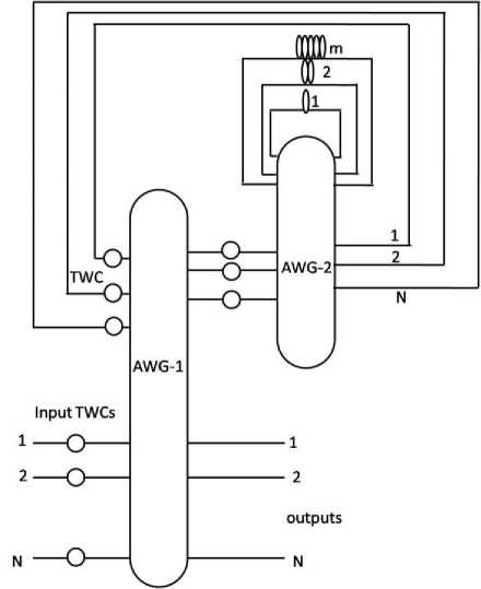
Fig. 1: Schematic of the architecture A1
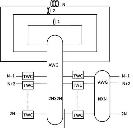
Fig. 2: Schematic of the architecture A2
This paper is organized as follows; in section II related work is presented. In section, III switch architecture is detailed. In section IV, comparative study with earlier architecture is presented. The placement of the switch in the network is detailed in section V. The major conclusions of the paper, is presented in section VI.
-
II. Related Work
-
2.1 Switch Architecture
In general optical network is composed of core and client network as shown in Fig. 3. The information generated in the client network is aggregated at the boundary of the optical cloud, via edge router. The backbone network is optical in nature, and optical router, route the packets in the optical domain. The design of the optical router is very important, and they are also known as optical packet switches. In this section, an overview of different optical switches is presented.
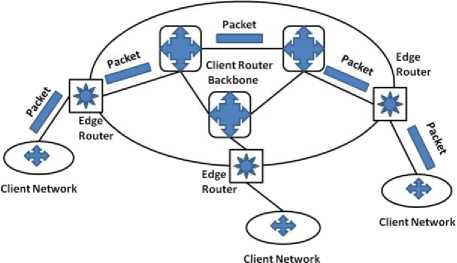
Fig. 3: Overlay structure of the network
Different photonic packet switch architectures have been proposed and demonstrated in past all these architectures use photonic means to perform packet buffering and routing; electronics plays the important role in functions such as, address processing, routing and buffering control.
Optical packet switch architectures in the broad sense can be classified into three categories such as.
-
1 ) Wavelength routed photonic packet switch
-
2 ) Broad-cast and select type switch
-
3 ) (AWG) / Space switch based packet switch
-
2 .1.1 Wavelength Routed Photonic Packet Switch
-
2 .1.2 Broad-Cast and Select Type Switch
-
2 .1.3 AWG/Space Switch Based Architectures
In this class of switches, wavelength coding is used for buffering and routing of packets. The switch consists of three functional blocks: a packet encoder block, a buffering block and packet demultiplexer block. The encoder block, encode the wavelengths of the incoming packets, buffering block buffer the encoded packets, if necessary and demultiplexer block, separate the packets and direct them to the appropriate output ports.
In this approach, at the input of the switch all the information is multiplexed by a star coupler, and distributed to all the output. Each receiver selects a particular packet only. Both TDM and WDM can be applied in these switches.
In this category, contending packets are stored in fiber delay lines using WDM technology. The various loop buffer based architectures are proposed [6-15]. All of them have their advantages and disadvantages and well described in their respective references. The first loop buffer based architecture is proposed by Bendelli [6]. This architecture requires a very large number of components for buffering; effectively Semiconductor Optical Amplifier (SOA) scales linearly with required number of buffer wavelengths, and also the size of the Demux and Mux have to be increased proportionally. Thus physical loss of the architecture is very large. Same problems are also associated with other architectures [7] [8]. The architecture proposed by Choa [9], have similar buffer structure, and in this architecture direct packets which require no delay also pass through the buffer Demux. Thus scaling is more critical in this architecture.
The third class of architecture uses AWG as a router. The insertion loss of the AWG router is very less as compared to splitter and combiner. Thus using AWG comparatively large number of users can be accommodated. The various AWG / Space switch based architectures are proposed [1] [2] [5] [16] [17] [18] [19]. In broad sense these architecture performs better than the re-circulating type loop buffer architecture.
In this paper an AWG based optical packet switch architecture is considered and it comparison is made in terms of packet loss probability and optical cost.
-
III. Architectures Description
The architecture presented in [5] which has feedback architecture (A1) shown in Fig. 1 require two AWGs. It uses shared feedback delay lines to buffer the contended packets.
ToAWG FromAWG
Fig. 4: Structure of type-2 module
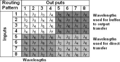
First, input packets are converted to the appropriate wavelengths and the contended packets are routed to the re-circulating loops for buffering while the straight-through packets are routed to switch outputs. The switch consist of N modules one for each output port and for a tagged output at maximum m packets can be stored. Hence, in all the modules at maximum N packets can have same delay varying from 1 to m slots and in all the modules mN number of packets can be stored. The architecture can be simplified by proper re-structuring. In the architecture A2, (Fig. 2) the upper N ports of the AWG router (scheduling section) ranging from 1 to N connect to N buffer modules. The lower ports (N+1 to 2N) of the AWG acts as actual inputs/outputs port of the switch which is equipped with TWCs and tune the wavelengths of the incoming packets as per the desired output ports. Suppose a packet arrives at the input i and destined for output j, and requires a delay of K slots. Then packet has to be pushed towards module K connected to theK port of the AWG. AWG is a cyclic wavelength router. The packet entering at the input port i can be routed to the output port K of the AWG by following the routing pattern of AWG, l = [1 + (i + k - 2) mod N ]
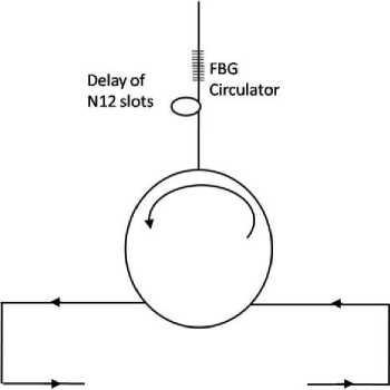
after the delay of K slots packet will again appear at input of the scheduling AWG and get routed to output i of the AWG due to its symmetric nature and packet can be directed to the appropriate output (j) by tuning the wavelength through TWC in the switching section, by following routing nature of switching section AWG [20]. In the buffer, module 1 provides a delay of one slot, module 2 provide a delay of two slots and so on. Thus as per the required amount of delay packets can be placed in different modules. In each buffer module, only one packet per output port will be stored. Thus at most N packets can be stored for a particular output port in all the modules and in each module N wavelengths are used. This will allow storing/ erasing of N packets in single time slot, one corresponds to each output. Referring, Fig. 1 it can be calculated that, between consecutive modules, N-1 wavelengths are common. Therefore, in N modules 2N-1 wavelengths will be required. Here, two types of buffer modules are considered. In the first type only pieces of fiber are used in the buffer, whose length varies from 1 to N slots (Fig. 2). The second type of buffer module (Fig. 3) consists of one optical reflector, one circulator and pieces of fiber with length varies from 1/2 to N/2 slots. This reduction in length is useful for large size packets, where buffer delay line length can grow up to some kilometers. Optical reflector used in the different modules can be dielectric mirror, thin film based mirror and fiber Bragg grating (FBG) etc. The full description of the multi-wavelengths FBG is given in [21] where it is shown that, a large number of wavelengths can be reflected from a single grating with reflectivity in the entire band as high as 99.8 percent with negligible insertion loss.
The working of the architecture is explained by considering N =4 i.e., 4×4 switch. In Fig. 5, routing pattern of the scheduling AWG of size 8×8 is shown and sets of wavelengths used for different types of routing. Here different modules are connected to upper ports 1-4 only, and port number 5-8 are actual inputs/outputs of the switch. The module which is connected to port 1, 2, 3 and 4 provides the delay of one, two, three and four slots respectively. Referring Fig. 6(a), in case of N =4, suppose a packet arrives at the input port 7 (scheduling section) for the output port 4 (switching section), and requires a delay of 3 time slots, then its wavelength will tuned to λ 1 as shown in Fig. 6(b), and will get routed to output port 3 of the scheduling AWG. In the first type buffer fiber delay will provide the delay of three slots. In the second type of the buffer modules, While traversing through the buffer packet will reach to the reflector placed in module 3 after 3/2 slots duration, here it will get reflected and there will be delay of 3/2 more slots. After the delay of three time slots the packet will appear at the input port 3 of the scheduling AWG and get routed to output port 7, due to the wavelength routing nature of the AWG. Thus packet appears at the input number 3 of TWC of the switching section which comprises AWG of size 4×4. Here, by converting its wavelength to λ 2 packet can be directed to the output port 4 (Fig. 6(b)).
used for transfer to buffer
Fig. 5: Routing pattern of 8×8 AWG router (scheduling section)
|
Routing Pattern |
Delay |
||||
|
1 |
2 |
3 |
4 |
||
|
И Q. E |
5 |
As |
As |
a7 |
As |
|
6 |
А/ |
As |
Ai |
||
|
7 |
А/ |
As |
At |
Аз |
|
|
8 |
As |
Ai |
Аз |
Аз |
|
(a)
|
Routing Pattern |
Out puts |
||||
|
1 |
2 |
3 |
4 |
||
|
и Q. E |
1 |
At |
Аз |
Аз |
Ад |
|
2 |
Аз |
Аз |
М |
Ai |
|
|
3 |
Аз |
Ад |
Ai |
Аз |
|
|
4 |
Ад |
Ai |
Аз |
Аз |
|
(b)
Fig. 6: (a) Schematic of wavelength routing as per the delay (b) Routing pattern of 4×4 AWG router (switching section)
The complete operation of the switch is controlled by a centralized electronic controller as shown in Fig. 7.
To Switching TWCs
FIFO 2
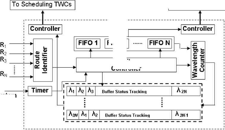
Fig. 7: Schematic of the control structure
Write Controller
System Clock
At the input of the switch a small power is tapped and after O/E conversion fed to the electronic control unit where the route identifier circuit identifies the routes (buffer/direct path). In the next step, write controller decides the tuning wavelengths of the packets by analyzing the buffer status for the different outputs. Then controller sends the appropriate control signal at the right instants to the scheduling and switching TWCs. The header and payload of the packet are separated by guard band as they may be modulated at different bit rates.
-
3.1 Queuing Structure
-
3.1.1 Mathematical Model
In the considered architecture, separate queue is formed for each output; therefore, architecture can be modeled as output queued system. The length of the queue for the each output port will be decided by the number of modules with maximum queue length of N packets. The performance evaluation of the output queued system is well described in [22]. In output queued system, very low packet loss probability is attainable and these queues are formed in wavelength domain, hence additional hardware is not required.
In this architecture each output has a separate queue with maximum queue length, equal to m slots. The maximum storage capacity of the buffer is Nm . This can be modeled by output queue.
In the output queue analysis, [22] [23] a specific queue is considered. The analytical results for this queue are also valid for all other queues as all of them are equivalent to each other. In this model assumes identical Bernoulli process. That is, in any time slot, probability of the arrival of packet on a particular input is p and each packet has equal probability 1/ N of being addressed to any of outputs. Defin ing a random variable X as the number of packet coming for a particular tagged output in a given slot the probability that exactly q packets will arrive in a slot is
[ q N - q
pl h -plN J I N J (2)
where
Let if Q i denote the number of packet in the tagged queue at the end of the ith time slot and X i denotes the number of packets arriving in the ith slot, then
Qi = minimax(0,Qi-1 + X -1), B} (3)
A packet will not be transmitted to the tagged output queue if Qi-1 =0 and Xi =0 in slot i . If in any time slot Qi-
1 +X i -1>B then Q i-1 +X i -1-B , packets will be lost at the input of the switch.
The markov chain model for the loop buffer is shown in the Fig. 8, and the state transition probability Pi j =Pr [ Qi=j|Qi- 1 =i ] can be written as
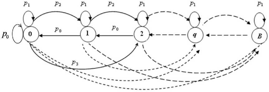
Fig. 8: Markov chain model
The performance evaluation of the output queued
system is well described in [23] using the same model the results obtained for packet loss probability under random traffic condition is shown in Fig. 9 for a switch
ij r j - 1 + 1 J J " J
of size N = 16 and m varying from 2 to 16. It can be visualized from the Fig. even at higher load (0.6) very
N m=j - i+1
(10-7)
10
otherwise
The steady state distribution of the markov chain can be obtained as
n Py = n
n = In П П n----nR | . ,
Where 0 1 2 3 B is the steady state distribution of the different state. The vector π should satisfy the following condition.
k
E ni =1
i = 1
low packet loss probability is attainable.
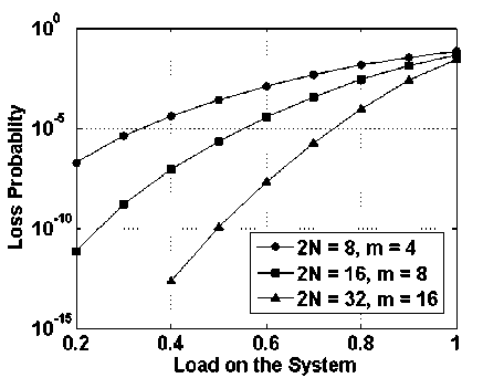
Fig. 9: Packet loss probability vs. load (Random Traffic) with varying number of buffer module
If we define normalized throughput ρ 0 , then
P0 = 1 - П0 P 0
The packet success probability can be obtained by dividing ρ0 by ρ . Here ρ is the offered load. Then packet loss probability can be obtained as
Pr[ Packet loss ] = 1 - P 0
P (7)
-
3.2 Bursty Traffic
In reality, packets arrive in the form of burst, and to observe the performance of the switch under co-related arrivals, the performance of the switch under bursty traffic is evaluated.
As a function of time, the traffic will be composed of bursts of packets destined to the same output port. These bursts are followed by an idle period that can be of length zero, where new burst will be adjacent to the older one (Fig. 10). The bursty traffic is characterized by two parameters
-
1) Average offered traffic load p , and
-
2) Average burst length, BL .
Time correlation of traffic on each input can be modeled as the Markov chain shown in Fig. 11. The chain is composed of two states: idle state (0) or burst state ( j ). The system will be in the idle state (0) when no packet arrives in the current slot. Also, if no packet will arrive in the next slot with probability Pa then a new burst will begin with probability 1- Pa and the system
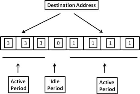
Fig.10: structure of busty traffic
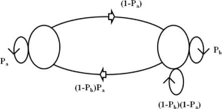
Fig. 11: Markov chain model for Busty traffic
will be transferred to the burst state j . In this state, one of the values of output destinations is chosen with equal probability. Being in this bursty state, the next arrival will be either the part of same burst with probability P b (i.e., destined to the same output port) or the burst will terminate. The termination of a burst can occur in two ways with certain probability:
-
1) Either a new burst will start for another destination.
This transfers the system to state other than the current one. The choice of another destination is equi-probable. The probability of this state will be (1- P b ) x (1- P a У
-
2) Or, going to the idle state with probability (1 - P b ) X P a .
The steady state equation for this Markov chain can be written in terms of steady state probabilities as,
P
a
(1 — P a )
(1 — P b ) P a ^
(1 — P a )(1 — P b ) + P b j
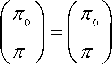
Here, n is the steady state probability of the system being in any one of state j i.e., n = 5 n j and 1 < j < N. Further using the property that summation of all the state probabilities is equal to unity, n0 + n = 1
Solving (8) and (9), we will get the steady state probabilities in terms of Pa and P b .
„ = P a (1 - Pb ) n = <1 - P >
-
0 1 -PP . 1 -PP,
ab and ab(10)
The average offered traffic load ( p ) will be a fraction of time the system is not in the idle state i.e.,
1 - P p = 1 - n =—
0 1 - PP
The probability of a burst of length k is
Hence the average burst length is
BL = ^^ k Pr( k ) = k = 1
1 - P b
Considering some fix value of p and BL in (11) and (12) respectively, the value of Pa and P b can be calculated and it will be used to simulate the performance of the above mentioned switch architectures under bursty traffic conditions.
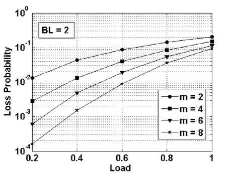
Fig. 12: Packet loss probability vs. Load (Busty Traffic)
The packet loss probability performance of the switch under the bursty traffic conditions while considering burst length (BL) is equal to two and switch size N = 8 with varying number of modules in shown in Fig. 12. It can be observed from the Fig. packet loss probability improves with number of modules, even under the bursty traffic conditions the packet loss probability is under acceptable limit.
-
IV. Comparative Study
In architecture A1 Along with this control algorithm for the switch is very complex. Controlling will required at three places i.e., input TWCs and two buffer TWCs. In the architecture A2, structure and the routing algorithm is very simple, physical loss of the buffer is negligible and control will only be required only at the input and output of the scheduling AWG. The unique feature of the architecture is that no controlling is required inside the buffer and using WDM a large number of packets can be stored in a single strand of fiber. The only advantage of the architecture A1 is that it is re-circulating in nature, but the re-circulation is only possible when,
-
1) no incoming packet will contend with buffered packet for the same TWC placed before AWG in single time slot (TWC before buffer AWG would be free)
-
2) No buffered packet tries to leave the buffer AWG in same time slot (TWC after buffer AWG would be free). Therefore, re-circulation operation is only possible when both the buffer TWCs are free. This problem in [5] is defined as exit time contention and they also modeled the switch for the tagged output queue system and derived a probabilistic expression for no exist time contention. In our opinion, under low loading condition, this recirculating feature will not be required and at higher load above stated conditions (1-2) cannot be avoided. Therefore, the re-circulating nature will add to the control algorithm complexity without gaining too much. In the architecture A2 we can get rid of N TWCs, which are costly component still packet loss probability will remain nearly same.
-
4.1 Cost Analysis
The optical cost measure is considered as parametric estimate of cost, scalability and hardware requirements. The methodology and optical cost of various components follows form [24] where optical cost of the different components is obtained by counting fiber to chip coupling (FCC). But the cost of TWCs is considered to be 4 as FCC does not include the wavelength conversion range. To incorporate the effect of wavelength conversion a generalized cost model is proposed in [25] where the cost of the TWCs is given by the expression
C TWC = ad b (14)
Here, a is normalization constant and d is the conversion range and 0.5 — b — 5.0 . The optical cost of the architecture A1 can be given as in
-
A1 TWC + AWG
b
+ L TWC + AWC
Substituting the cost values of different components, we get
-
C, = N ( 2 N - 1 ) b + 4 N
-
C, = N [ ( N + m - 1 ) b + ( 2 N - 1 ) b + б ] + 2 m (16)
and for N = m the cost of the architecture A1 will be given by
C j = N [ 3 ( 2 N - 1 ) b + 8
Similarly the cost of architecture A2 will be given by
Ca 2 = NCTwc + NCAwc + NctWc + NCAWc (18)
After inserting cost values we get,
C,= N (2N-1)b +(N-1)b + 6
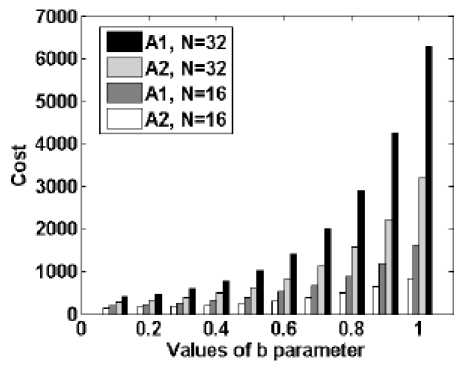
Fig. 13: Total Cost vs. b Parameter
In Fig. 13, cost of both the architectures is compared in term of Fiber-to-Chip Coupling (FCC) unit. Here, the cost of the optical fiber is neglected in both the architectures, considering N = 32 and b = 1 the cost values of architecture A1 and A2 will be 6304 and 3200 FCC units. Hence, in the architecture A2 cost of the architecture is reduced by 49.2 percent. Similarly for b = 0.5 the cost of architecture A1 is 1018 and that of architecture A2 is 624 and hence cost reduction is 39 percent. Therefore, cost analysis suggest that addition of few more fiber delay lines is better option rather than achieving re-circulating nature through buffer TWCs (Architecture A1) under the assumption of no exit time contention.
-
V. Placement of the Switch in Network
5.1 The Loss Analysis
Referring the Fig. 3, the switches will be placed in the backbone networks, where multiplexed data traverses from one node to other. As multiplexed data will arrive at the switch input, it should be first demultiplexed, however, as the data can arrive at any wavelength range, splitter should be used at the input, and combiner at the switch output. The modified architecture is shown in Fig. 14.
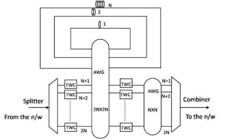
Fig. 14: Schematic of the modified architecture
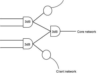
Fig. 15: Schematic of the combiner with dropping to client n/w
The use of combiner also allow us to drop the data at a particular switch and from where, it can be routed to client network (n/w) (Fig. 15).
As splitter and combiner are lossy device, i.e., their insertion loss is large as compared to other devices. Therefore, the overall loss of the switch increases, and hence when data traverse through the switch suffers from severe switch loss. The loss of the switch can be calculated as
L (S) = L + i . + LAW
AWG
+ TWC + S^Sw + ^combiner where, i is the loss of the (i=type) device. Considering for example a 4 x 4 switch, the total loss is given by
In the above calculation it must be remembered that the size of scheduling AWG is 8×8. Hence if data pass through the switch it will suffer a loss of 20.5 dB, which is huge loss. Therefore, it is required to compensate such a huge loss with an optical amplifier like EDFA (Erbium doped fiber amplifier).
If EDFA is placed inside the switch, in such a case EDFA will be placed in each branch of the (scheduling/switching) port or placed in the each module of the buffer. But such arrangement will be a loss of hardware and cost, as only one amplifier can amplify more than one signal simultaneously. Hence, it is advisable that the amplifiers should be placed in the n/w between two cascaded switches as for example the placement of the amplifier is shown in Fig. 16.
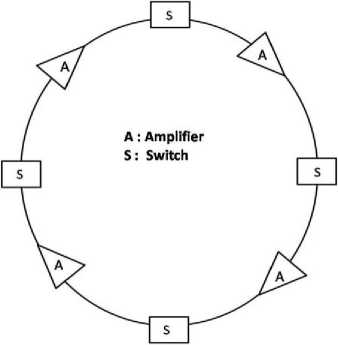
Fig. 16: Placement of Amplifier in Ring Network
-
VI. Conclusions
In this paper, optical packet switch architecture is discussed, which is realized using components like optical reflectors, tunable wavelength convertor (TWC), arrayed waveguide grating (AWG) and pieces of fiber. This architecture uses routing pattern of AWG, and its symmetric nature, to simplify switch operation significantly. In the presented architecture, large number of packets can be stored in a single fiber delay line and in the buffer, controlling of the packets is not required. Finally, modifications in the architecture are suggested that will enable its placement in optical network.
References AWG Based Optical Packet Switch Architecture
- R. S. Tucker and W. D. Zhong., ”Photonic packet switching: an overview,” IEICE Trans. Commun., vol. E82 B, no.2, pp. 254-264, Feb. 1999.
- R. K. Singh, R. Srivastava and Y. N. Singh, ”Wavelength division multiplexed loop buffer memory based optical packet switch,” Optical and Quantum Electronics, vol. 39, no. 1, pp. 15-34, Jan. 2007.
- A. Pattavina, ”Multi-wavelength switching in IP optical nodes adopting different buffering strategies,” Optical Switching and Networking, vol. 1, no. 1, pp. 65-75, Jan. 2005.
- D. K. Hunter, M. H. M. Nizam, M. C. Chia, I. Andonovic, K. M. Guild, A. Tzanakaki, M. J. O’Mahony, L. D. Bainbridge, M. F. C. Stephens, R. V. Penty and I. H. White, ”WASPNET: A wavelength switched packet network,” IEEE Commun. Magazine, vol. 37, no. 3, pp. 120-129, Mar. 1999.
- M. C. Chia, D. K. Hunter, I. Andonovic, P. Ball, I. Wright, S. P. Ferguson,K. M. guild and M. J. O’Mahony, ”Packet loss and delay performance of feedback and feed-forward arrayed-waveguide gratings-based optical packet switch with WDM inputs-outputs,” J. Lightw.Technol., vol. 19, no. 9, pp. 1241 -1254, Sep. 2001.
- R. Srivastava, R. K. Singh and Y. N. Singh, “Design Analysis of Optical Loop Memory,” J. Lightw. Technol. vol.27, no. 21, pp.4821-4831, Nov.2009.
- W. D. Zhong and R. S. Tucker, “A wavelength routing based photonic packet buffer and its application in photonic packet switching systems,” J. Lightw. Technol., Vol. 16, No. 8, pp. 1737-1745, Oct. 1998.
- K. Sasayama, et.al., “FRONTIERNET: Frequency routing type time division interconnection network,” J. Lightw. Technol., Vol. 15, No. 10, pp. 417-429, Mar. 1997.
- Y. Shmimazu and M. Tsukada,“Ultrafast photonic ATM switch with optical output buffers,” J. Lightw. Technol., Vol. 10, pp. 265-272, Feb. 1992.
- G. Bendelli, et.al., “Photonic ATM switch based on multi-wavelength fiber loop buffer,” OFC’95, Vol.8, pp.141-142, Feb.1995.
- R. Srivastava, R. K. Singh and Y. N. Singh, “Optical loop memory for photonic switching application,” OSA J. of Optical Networking, vol. 6 pp. 341-348, Apr 2007.
- N. Verma, R. Srivastava and Y. N. Singh, “ Novel design modification proposal for all optical fiber loop buffer switch,” in 2002 Proc. Photonics Conf., p. 181.
- Y. N. Singh, A. Kushwaha and S. K. Bose, “Exact and approximate modeling of an FLBM-based all optical packet switch,” IEEE J. of Lightw. Technol., vol. 21, pp. 719-726, Mar. 2003.
- F.S.Choa, et.al., “An optical packet switch based on WDM technologies,” IEEE J. of Lightw. Technol., vol. 23, pp. 994-1013, Mar. 2005.
- H. Nakazima, “Photonic ATM switch based on a multi wavelength fiber loop buffer,” CSELT tech. Rep. Vol. 23, pp. 331-335, 1995.
- R. Srivastava, R. K. Singh and Y. N. Singh, “Regenerator based optical loop memory,” In Proceedings IEEE TENCON Region 10 Conference, Taiwan, ROC, 2007, paper no.WeOE-O2.3.
- R. Takabashi, et.al., “Photonic random access memory for 40- Gbps 16-b burst optical packets,” IEEE Photon Technol. Lett. Vol.16, No. 4, pp. 1185-1187, Apr. 2004.
- C. M. Gauger, et.al, “Optimized combination of converter pools and FDL buffers for contention resolutions in optical burst switching,” Photonic Netw. Commun. Vol. 9, No. 2, pp. 139-148, Sep. 2004.
- C. Guillernot et.al., “Transparent optical packet switching: the European ACTS KEOPS project approach,” J. Lightw. Technol. Vol. 16, No. 12, pp. 2117-2134, Dec.1998.
- R. Srivastava, R. K. Singh and Y. N. Singh, ”All optical reflectors based WDM Optical Packet Switch,” Indian Patent office, patent application no. 2707/DEL/2007 (patent filed).
- Q. Wu, P. L. Chu and H. P. Chan, ” General design approach to multichannel fiber Bragg grating,” J. Lightw. Technol., vol. 24, no.3, pp. 1571- 1580, Mar. 2006.
- M. J. Karol, M. G. Hluchyj, and S. P. Morgan, “Input versus output queuing on a space-division packet switch,” IEEE Trans of commun., 35, 1347-1356 (1987).
- M. G. Hluchyj, and M. J. Karol, “Queuing in high performance packet switching,” IEEE J. sel. areas commun. 6. 1587-1597 (1988).
- R. V. Caenegem, ”From IP over WDM to all-optical packet switching: economical view,” J. Lightw. Technol., vol. 24, no. 4, pp. 1638-1645, Apr. 2006.
- V. Eramo, M. Listanti and A. Germoni, ”Cost evaluation of optical packet switches equipped with limited-range andfull-range converters for contention resolution,” J. Lightw. Technol., vol. 26, no. 4, pp. 390-407, Feb. 2008.
