Current Trends of High capacity Optical Interconnection Data Link in High Performance Optical Communication Systems

Author: Ahmed Nabih Zaki Rashed
Journal: International Journal of Intelligent Systems and Applications(IJISA) @ijisa
Article in issue: 3 vol.5, 2013.
Free access
Optical technologies are ubiquitous in telecommunications networks and systems, providing multiple wavelength channels of transport at 2.5 Gbit/sec to 40 Gbit/sec data rates over single fiber optic cables. Market pressures continue to drive the number of wavelength channels per fiber and the data rate per channel. This trend will continue for many years to come as electronic commerce grows and enterprises demand higher and reliable bandwidth over long distances. Electronic commerce, in turn, is driving the growth curves for single processor and multiprocessor performance in data base transaction and Web based servers. Ironically, the insatiable taste for enterprise network bandwidth, which has driven up the volume and pushed down the price of optical components for telecommunications, is simultaneously stressing computer system bandwidth increasing the need for new interconnection schemes and providing for the first time commercial opportunities for optical components in computer systems. The evolution of integrated circuit technology is causing system designs to move towards communication based architectures. We have presented the current tends of high performance system capacity of optical interconnection data transmission link in high performance optical communication and computing systems over wide range of the affecting parameters.
Optical Fiber Link, High Speed Optical Interconnection, Integrated Optics, Optical Source, Optical Detector
Short address: https://sciup.org/15010394
IDR: 15010394
Text of the scientific article Current Trends of High capacity Optical Interconnection Data Link in High Performance Optical Communication Systems
Published Online February 2013 in MECS
Optical interconnections on silicon have been extensively investigated in recent years as interconnections become the bottleneck for the nextgeneration computing systems [1]. The goal of these investigations is to provide a compact, low power consumption, high bandwidth and low-latency optical interconnection system with full CMOS compatibility. Silicon based optical components such as low-loss silicon-on-insulator (SOI) optical waveguides [2], high speed silicon modulators, and Germanium on SOI detectors enabling large-scale optical integration on a silicon chip. While most attention is focused on single channel systems at this stage, wavelength division multiplexing (WDM) technology is necessary to fully utilize the ultra wide bandwidth of the optical interconnection medium, given that the transmission bandwidths of both silicon waveguides and optical fibers are on the order of 10 to 100 THz. As the key components of such a system, we show high speed and multi-channel modulation using cascaded silicon micro ring modulators [3].
Optical transparency is widely recognized to play a central role in next-generation optical networks and to offer significant networking advancements in terms of performance and cost [4]. The scalability of optical technology and the elimination of expensive optical-electrical-optical (OEO) equipment is expected to significantly reduce the capital costs, whereas operational cost savings are expected to result from reduced power requirements and the flexibility of transparent service provisioning. The first steps toward this goal were point-to-point links routed via optical add–drop multiplexers (OADMs) at intermediate nodes, and increasingly the trend is toward so-called islands of transparency, with the eventual aim of fully meshed transparent optical networks with reconfigurable optical cross connects (OXCs) [5]. For the wavelength division multiplexing interconnection systems, in addition to the low power consumption and small size, ring modulators have another advantage: they modulate only light at particular wavelengths (the resonant wavelengths of the ring resonators) and allow light at all other wavelengths to pass through the modulators without been affected. Therefore, one can cascade several ring modulators with different resonant wavelengths on a single waveguide, and modulate different wavelengths of light independently [6].
In the present study, we have investigated the high capacity optical interconnection systems within actual operating bandwidth, signal to noise ratio at the receiver point, classical and Shannon transmission bit rates and products of both silica-doped and plastic materials based waveguides over wide range of the operating parameters.
-
II. Simplified Architecture for WDM Optical Interconnection System
As shown in Fig. 1 presents a simple architecture for a WDM interconnection system. A similar structure has been proposed for polymer modulators [7]. Light from a WDM source or a broadband source is sent into a silicon waveguide coupled to multiple ring modulators with different resonant wavelengths. If the input is a wavelength division multiplexing source, the resonant wavelength of each modulator needs to match the wavelength of each channel of the wavelength division multiplexing source. At the receiver side, these channels can be demultiplexed using similar ring resonators with drop ports, and detected separately. If the input is a broadband source, it only requires that the resonant wavelengths of the ring modulators match one-to-one with those of the ring demultiplexers [8, 9].
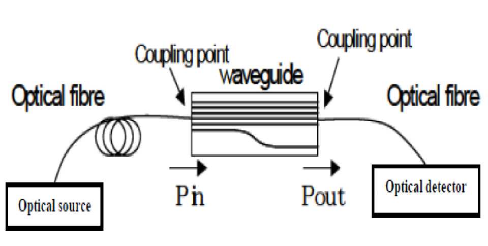
Fig. 1: WDM Optical interconnection system
-
III. Theoretical Model Analysis
In order to quantify the requirements for drive current for satisfactory laser modulation performance, the optical pulse data stream is fed into a thermal noise dominated simple photodiode receiver (50 Ω load) through 6 dB of optical loss (a typical number in short transmission distance optical interconnect). The received photocurrent after equalization at the receiver has the simple form [10].
2 Гn Bt ] h ( t ) = n iink I m cos | — I ,
Where I m is the drive current to the laser, B is the transmission bit rate, the link efficiency (η link ) includes the laser differential quantum efficiency (0.3 Watt/A), the link loss (6 dB), and the detector responsivity (0.5 A/Watt). The required drive current to maintain a BER of 10-9 as a function of the laser threshold current. The bit error rate at the receiver can be:
error function. For each data point the decision level (D) is numerically chosen to minimize the corresponding BER. Where the distribution function of turn on time of the laser (t on ) can be expressed as:
-n n I ton I p (ton ) I 1 I ton V t0 )
This required drive current is used to calculate the average electrical power consumption for the laser given by the following formulas:
P E = 0-5 I m ( ^ 0 + I m Z 0 ) ,
The initial carrier number in the laser n depends on the number of “0” bits which precede the “1” bit. At the end of a bit, the carrier number decays exponentially with time constant τ such that:
Г- NT ni = nth exP I ------
V T
ГГ ( „
BER = 0.25 ere-^ +
VV v
t 0
J
Г . . г
P ( t on ) erf
V V

d ( t on )
Where D is the decision level, σ is the variance of the thermal noise, and erfc(x) is the complementary
Where N is the number of “0” bits preceding the considered transmission bit, nth is the threshold carrier number, τ is the carrier life time and T = 1/B. The threshold current and turn on time of the laser can be expressed by [11]:
nth e
I th =------ ,
т ton
Where e is the electronic charge, t 0 = T Ith / I m , and the coupling efficiency from optical source to the optical link is:
n iink = In ( 2 ) B T
3.1 Materials based connector
A 1 = 0.691663+0.1107001* x, A 2 = (0.0684043+0.000568306 * x)2 * (T/T 0 )2, A 3 = 0.4079426+0.31021588 * x,
A 4 = (0.1162414+0.03772465 * x)2 * (T/T 0 )2, A 5 = 0.8974749-0.043311091 * x, and A 6 = (9.896161+1.94577 * x)2. Where T is the ambient temperature in ºC, T 0 is considered to be as 25 ºC (room temperature), and x is the ratio of germania dopant added to silica material to improve its optical performance characteristics within the range of 0.0 ≤ x ≤ 0.3 [14]. Also the plastic cable core material which the investigation of the spectral variations of the waveguide refractive-index (n) requires Sellemeier equation under the form [15]:
A connector is used to join a fiber cable to a transmitter or receiver, or is used to join together strands of fiber link. A connector for fiber is similar in concept to a traditional electrical connector, but the fiber connector is actually more delicate, as it must precisely align the internal fibers to insure a proper flow of data through the cables. For single mode fibers (SMF), the Fresnel reflection loss caused by the differences between the refractive indeces of the silica doped and plastic fibers and the material separation are given as the following [13]:
n 2
, B л 2 B3 л 2 B5 л 2
, 2 д2 ,2 д2 ,2 д2
л — B 2 л — B 4 л — B 6
For the plastic material, the coefficients of the Sellmeier equation and refractive-index variation with ambient temperature are as: B 1 = 0.4963, B 2 = 0.6965 (T/T 0 ), B 3 = 0.3223, B 4 = 0.718 (T/T 0 ), B 5 = 0.1174, and B 6 = 9.237 (T/T 0 ).
Lc = 20 log
4 n n clad
(n + nc/ad)2 J clad dB/cm
Where n is the refractive-index of silica-doped or plastic materials. The cladding refractive index can be expressed as a function of both silica-doped and plastic core refractive indices and relative refractive-index difference as the following:
n clad = ( 1 — A n ) n
3.2 Materials based optical waveguide
Special emphasis is given to the transmission characteristics of silica-doped and plastic fibers as promise links in long and short distance optical communications. Silica-doped and plastic waveguide characteristics (spectral loss and chromatic dispersion) are thermal dependent, thus, these two variables must be taken into account when studying the transmission bit rate capacity of the waveguides over wide range of the operating parameters.
Then by substituting from Eq. (10) into Eqs. (9), we can obtain:
Lc = 20 log
' 4 ( 1 — A n ) n 2 '
l>
—
A n • n ) 2 ,
' ' dB/cm
3.2.1 Silica-doped material based waveguide
Based on the models of [14], the spectral losses of silica-doped waveguides are cast as:
а = « I + « s + « uv + « [r , dB/cm
The relative refractive-index difference Δn for both silica-doped and plastic materials are given by:
Where
« I = the int rinsic loss = 3 x 10 8
dB/cm,
n
A n = —
—
n clad
,
n
and(16)
( 0.75 + 66 A n )f T )
« S = Rayleigh scattering = I — ---—— II — I ,
( л x 10 Л T 0 J dB/cm (17)
The refractive-index of silica-doped material
waveguide based on [14]:
Sellemier equation is given by
2 , A л 2
n 2 = 1 + 2 1 2
л 2 — A 2
A 3 л А 5 л 2
+ л 2 — A 4 2 + л 2 — A 2
Where the scattering loss is linearity is related to the ambient temperature Τ, T 0 is a reference temperature or room temperature and is taken as value of 25 ° C, An and λ are the relative refractive index difference and operating optical signal wavelength respectively. The absorption losses α UV and α IR are given as [14]:
The Sellmeier coefficients of the refractive index of this waveguide are cast as [14]:
« UV = 1.1 x 10 9 to ge %
4.9л e , dB/cm
a IR = f 7 x 10 - 10 e
dB/cm
dn
"dA
f A I f B 1 B 22 + B 3 B 42 + B 5 B 62 '
n bA La bA La bA
V J V ( A — B 2 ) ( A — B 4 ) ( A — B 6 ) J
Where ω ge % is the weight percentage of germania, GeO 2 added to optical silica fibers to improve its optical transmission characteristics. The percentage of germania ω ge % and the mole fraction x are cast under the form:
« „ % = 213.27 x — 594 x 2 + 2400 x 3 - 4695 x 4
ge 0
The first and second differentiation of Eq. (13) with respect to operating signal wavelength λ which yields:
dn dA
—
A
n
V
J A 1 A 2 A 3 A 42 A 5 A 2
H( a — A 22 1 A — A .f A — A 2 ) 2 J
d2n dA2
—
n
VJ
V
Л
d n2L12 . n2^ n d2Li2 . n2^ n п2^12 . n2^(
B1B2 (3A + B2), B3B4 (3A + B4), B5B6 (3A + B6)
++
,2 „23 .,2 „23 .,2 „23
A — B2) (A — B4) (A — B6)
3.3. Classical transmission bit rate
d 2 n d A
—
V J
(
V
AA 2 ( 3 A 2 + A 2 ) AA 2 ( 3 A 2 + A 2 ) AA 2 ( 3 A 2 + A 2 ) f dn I
1 2 У 2 I + 3 4 у 4 j + 5 у 6 j — ____ A 2 — A 2 2 f ( я 2 — A 42 f ( A 2 — A 6 2 1 3 J V d A J ’
A
3.2.2 Plastic material based waveguide
Plastics, as all any organic materials, absorb light in the ultraviolet spectrum region. The mechanism for the absorption depends on the electronic transitions between energy levels in molecular bonds of the material. Generally the electronic transition absorption peaks appear at wavelengths in the ultraviolet region, and their absorption tails have an influence on the plastic optical fiber (POF) transmission loss [15]. According to urbach’s rule, the attenuation coefficient α e due to electronic transitions in POF is given by [15]:
a e ( plastic ) = 1.10 x 10
— I
10 f 8 I exp It I ,
V A J dB/cm
Where λ is the optical signal wavelength of light in μm and . In addition, there is another type of intrinsic loss, caused by fluctuations in the density, and composition of the material, which is known as Rayleigh scattering.. This phenomenon gives the rise to scattering coefficient a R that is inversely proportional to the fourth power of the wavelength, i.e., the shorter is λ the higher the losses are. For POF, it is shown that aR is given by [15].
a R ( plastic ) = 13 x 10 5
' 0.633 1 4
. A J
dB/cm
Then the total losses of plastic optical fibers are given by:
a ( plastic ) = a e ( plastic ) + a R ( plastic ) jg/cm (25)
The first and second differentiation of Eq. (14) with respect to operating wavelength λ which yields:
J
,
The total pulse broadening due to material and waveguide dispersion in single mode fibers is given by:
Therefore, the total chromatic dispersion in standard single mode fiber that limits the transmission bit rates in system based optical communication can be calculated as follows [16]:
D t = —( M md + M wd ) ,
M md =
A d n AA d n
A c V "dA v
The waveguide dispersion coefficient is given by the following expression:
M wd =
— n c/ad f^ n J F ( V ) , V c A s J
Where n clad is the refractive-index of the cladding material, Δn is the relative refractive-index difference, X is the operating optical signal wavelength in pm, and F (V) is a function of V number or normalized frequency. Based on the work [16], they designed the function F (V) is a function of V as the following expression:
F ( V ) = 1.38 V — 6.98 V 2 + 13.45 V 3 — 4.84 V 4 — 1.48 V 5 ,
When they are employing V-number in the range of (0 < V < 1.15) yields the above expression. We are taking into account V-number as unity to emphasis single mode operation. Then the classical transmission bit rate as a function of waveguide length, total losses ( a ), and total pulse broadening ( А т) due to total chromatic dispersion is given by [16]:
а 5000 e " Lw
B(Transmission bitrate) = ,
3.4. Shannon transmission capacity
The signal to noise ratio (SNR) is a measure of signal quality at the receiver side, it is given by [16]:
SNR =-----------(GP0 P) Z0—--------
4 kTB W sig . + 2 eZ 0 B Wslg . G n ( Id + p P 0 )
( SNR ) dB = 10log SNR ,
Where P 0 is the received or output optical power, ρ is the detector’s unamplified responsivity, G is the detector gain if an avalanche photodiode (APD) is used, n accounts for the excess noise of the avalanche photodiode (usually between the value of 2 and 3), B.W sig. is the signal bandwidth at the receiver, k is Boltzmann’s constant (k = 1.38 x 10⁻²³ J/K), e is the magnitude of the charge on an electron (1.6 x 10⁻¹⁹ coulomb), T is the ambient temperature in ºC, ID is the detector’s dark current, and Z 0 is the resistance of the load resistor that follows the photodetector. The signal bandwidth and maximum transmission bit rate or capacity according to modified Shannon technique is given by [17]:
в Wsig = — ,
Дг^№ GHz(37)
br(sh)= BW,g.log2 (1+ SNR) ,Gbi„sec(38)
Where B.W sig. is the actual bandwidth of the optical signal and SNR is the signal to noise ratio in absolute value (i. e., not in dB). Where the Shannon bandwidthlength product within waveguide can be given by [18, 19]:
Where L w is the waveguide length, and B R (SH) is the Shannon transmission bit rate.
-
IV. Simulation Results and Discussions
We have analyzed parametrically, and numerically the high transmission bit rate and product of high capacity optical interconnection systems in modern communication and computing systems. Based on the modeling equations analysis and the assumed set of the operating parameters as shown in Table 1.
Table 1: Proposed operating parameters for optical interconnection model
|
Operating parameter |
Definition |
Value and units |
|
T |
Ambient temperature |
25 ºC ≤ T ≤ 45 ºC |
|
L W |
Waveguide length |
2 cm ≤ L m ≤ 5 cm |
|
P 0 |
Output power |
0.2 Watt ≤ P 0 ≤ 0.597 Watt |
|
T 0 |
Room temperature |
25 ºC |
|
X |
signal operating wavelength |
1.3 цт < X ≤ 1.65 μm |
|
Z 0 |
Series and load resistance |
100 Ω |
|
G |
Detector gain |
20 dB ≤ G ≤ 50 dB |
|
I D |
Detector dark current |
8 nA |
|
ρ |
detector responsivity |
0.25 A/Watt ≤ G ≤ 0.8 A/Watt |
|
A X |
Spectral line width of optical source |
0.1 nm |
|
V 0 |
Turn on voltage |
1 Volt ≤ V 0 ≤ 10 Volt |
|
A nsilica-doped |
Refractive index difference of silica-doped |
0.005 < A n ≤ 0.009 |
|
A nplastic |
Refractive index difference of plastic |
0.05 < A n < 0.09 |
|
n silica-doped |
Refractive index of silica-doped |
1.442 ≤ n ≤ 1.448 |
|
n plastic |
Refractive index of plastic |
1.494 ≤ n ≤ 1.554 |
|
t on |
Turn on time of the laser |
1 msec ≤ t on ≤ 10 msec |
|
τ |
Carrier life time |
2 nsec ≤ τ ≤ 10 nsec |
|
B |
Transmission bit rate |
1 Gbit/sec ≤ B ≤ 10 Gbit/sec |
|
I th |
Threshold current |
1 μA ≤ I th ≤ 50 μA |
|
I m |
Drive current of the laser |
0.1 mA ≤ I m ≤ 0.5 mA |
|
η Link |
Link efficiency |
60 % ≤ η ≤ 95 % |
|
c |
Speed of light |
3x10⁸ m/sec |
The following facts are assured as shown in the series of Figs. (2-27):
-
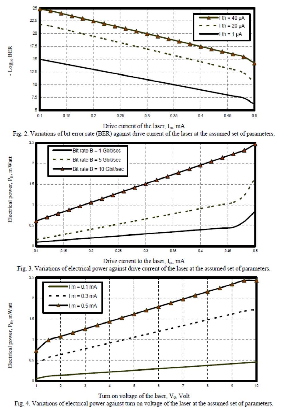
i) Fig. 2. has assured that as that as drive current of the laser increases, the bit error rate decreases at constant threshold current.
Moreover as threshold current increases, the bit error rate also increases at constant drive current of the laser.
-
ii) As shown in Figs. (3, 4) have demonstrated that as both drive current and turn on voltage of the laser increases, the electrical power also increases. As well as transmission bit rate increases, the electrical power also increases.
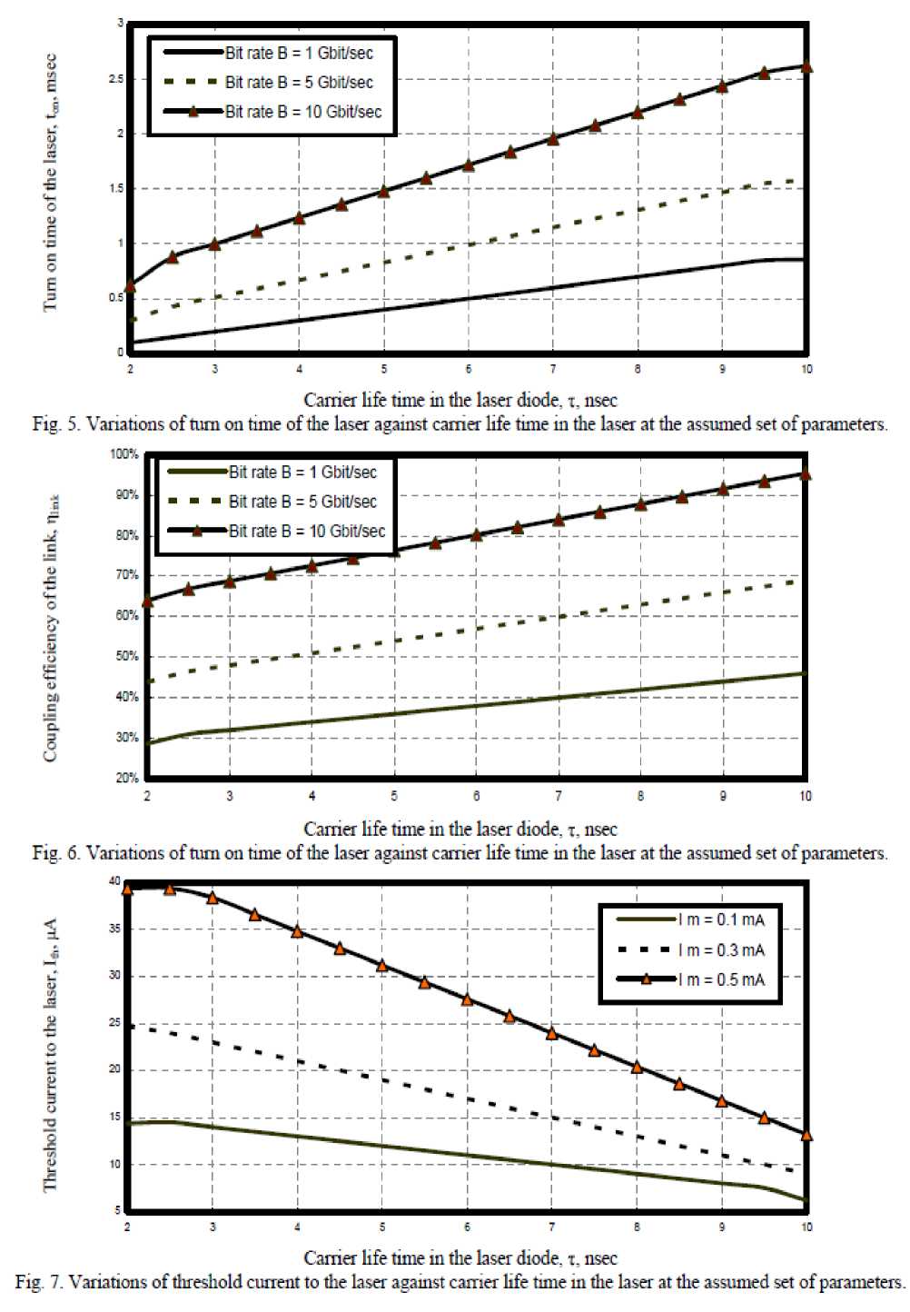
-
iii) Figs. (5, 6) have proved that carrier life time in the laser diode increases, both turn on time of the laser and coupling efficiency also increases at constant transmission bit rate. With increasing transmission bit rates, the turn on time of the laser and coupling efficiency to the waveguide must be increased.
-
iv) Fig. 7 has indicated that as carrier life time in the laser diode increases, the threshold current decreases at constant drive current to the laser. But as drive current to the laser increases, the threshold current must be increased.
-
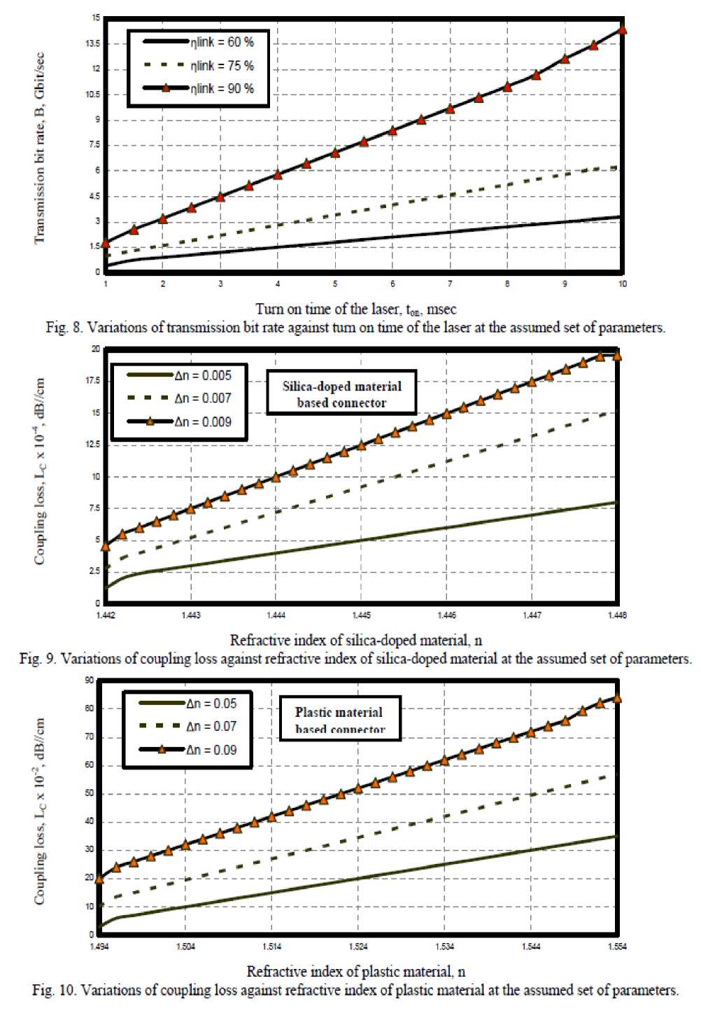
v) Fig. 8 has demonstrated that as both coupling efficiency of the laser to the optical link, and turn on time of the laser increases, the transmission bit rates also increase.
-
vi) As shown in Figs. (9, 10) have demonstrated that as both refractive index of silica-doped and plastic materials based waveguide, and relative refractive index difference increase, the coupling losses also increase. But we find the higher coupling loss for plastic material based waveguide.
-
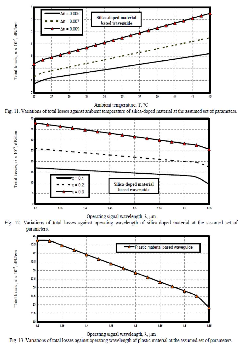
vii) As shown in Figs. (11, 12) have proved that as ambient temperature percentage amount of germanium and relative refractive index difference increase, the total losses of silica-doped material based waveguide also increase. But as operating signal wavelength increase, the total loss of silica-doped material based waveguide decreases.
-
viii) Fig. (13) has assured that as operating signal wavelength increase, the total loss of plastic material based waveguide decreases.
-
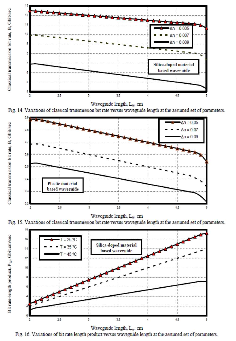
ix) Figs. (14, 15) have assured that as both
waveguide length and relative refractive index difference decrease, the classical transmission bit rate increases for both silica-doped and plastic materials based waveguide. We observed the increased classical transmission bit rate for silica-doped waveguide than plastic waveguide.
-
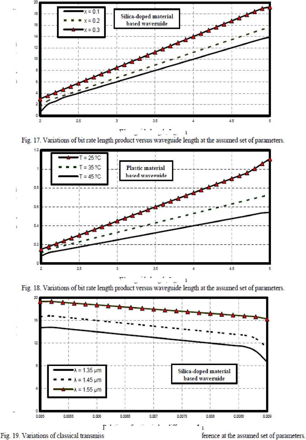
x) Figs. (16-18) have demonstrated that as waveguide length increases and ambient temperature decrease, the transmission bit rate-length product increases for both silica-doped and plastic materials based waveguide. We observed the increased classical bit ratelength product for silica-doped waveguide than plastic waveguide. Moreover as percentage amount of germanium increases, this leads to the increased bit rate length product within silica-doped material based waveguide.
-
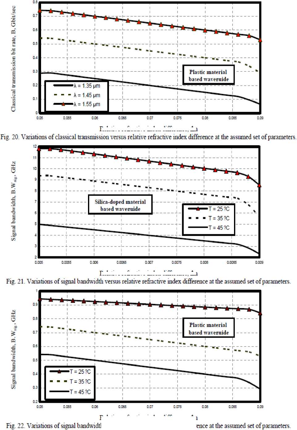
xi) As shown in Figs. (19, 20) have indicated that as relative refractive index difference decreases, and operating signal wavelength increases, the classical transmission bit rate increases for both silica-doped and plastic materials based waveguide. As well as we have observed the increased classical transmission bit rate for silica-doped material based waveguide than plastic material based waveguide.
-
xii) Figs. (21, 22) have assured that as both
ambient temperature and relative refractive index difference decrease, the signal bandwidth increases for both silica-doped and plastic materials based waveguide. We observed the increased signal bandwidth for silica-doped material waveguide than plastic material based waveguide.
-
xiii) As shown in Fig. (23) has indicated that as ambient temperature decreases and output power at the receiver point increase, the signal to noise ratio also increases for both silica-doped and plastic materials based waveguide.
-
xiv) Figs. (24-27) have assured that as signal to noise ratio increases and waveguide length decreases, the Shannon transmission bit rate increases for both silica-doped and plastic materials based waveguide. Moreover as both signal to noise ratio and waveguide length increase, this leads to increase of Shannon product for both silica-doped and plastic materials based waveguide.
Waveguide length. L», cm
Fig. 16. Variations of bit rate length product versus waveguide length at the assumed set of parameters.
Fig.
Fig.
Waveguide length, L,-. cm
Variations of classical transmission bit rate versus waveguide length at the assumed set of parameters.
Waveguide length. Lw. cm
Variations of classical transmission bit rate versus waveguide length at the assumed set of parameters.
Silica-doped material baied wavemiide
= 0.005
= 0.007
= 0.009
■An = 0.05
An = 0.07
An = 0.09
Plastic material based waveeuide
T = 25?C
T = 35?C
T = 45 ?C
Silica-doped material based waveenide
Relative refractive index difference. An
Waveguide length. L,. cm
Waveguide length, L^., cm
Relative refractive nidex difference. An
Relative refractive index difference. An
Relative refractive index difference. An
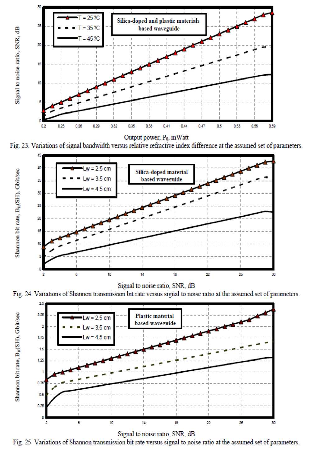
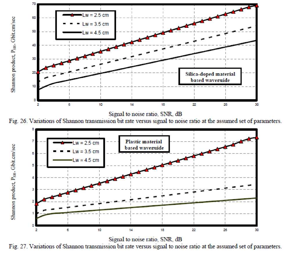
Fig.
Fig.
Signal to noise ratio. SNR. dB
Variations of Shannon transmission bit rate versus signal to noise ratio at the assumed set of parameters.
Silica-doped material based waveguide
= 2.5 cm
= 3.5 cm
= 4.5 cm
■Lw = 2.5 cm
Lw = 3.5 cm
■Lw = 4.5 cm
Plastic material based waveeuide
Signal to noise ratio. SNR. dB
Variations of Shannon transmission bit rate versus signal to noise ratio at the assumed set of parameters.
-
V. Conclusions
In a summary, we can conclude that the increased drive current to the laser, and turn on voltage of the laser, this leads increase of electrical power that limits the bit error rate. Also the increased carrier life time this leads to increase of transmission bit rate and coupling efficiency to the optical link. The decreased of both relative refractive index difference, and refractive index of silica-doped and plastic materials based connector, this leads to decrease coupling losses. The decreased of both ambient temperature, and percentage amount of germanium added to silica, and the increased operating signal wavelength, this leads to decrease of waveguide loss of silica-doped waveguide. As well as increase operating signal wavelength, this leads to decrease of optical loss of plastic material based waveguide. With decreasing of both ambient temperature, and relative refractive index difference and increasing of both signal to noise ratio, and waveguide length of both silica-doped and plastic materials based waveguide this leads to increasing of both classical bit rate-length and Shannon product for both materials based waveguide. It is evident that silica-doped material based both connector and waveguide present lower optical losses, and higher of both classical transmission bit rate, and product and Shannon transmission bit rate and product than plastic material based of both connector and waveguide.
References Current Trends of High capacity Optical Interconnection Data Link in High Performance Optical Communication Systems
- S. Sygletos, I. Tomkos, and J. Leuthold, “Technological Challenges on the Road Toward Transparent Networking,” J. Opt. Network, Vol. 7, No. 2, pp. 321–350, 2008.
- D. Fishman, D. L. Correa, E. H. Goode, T. L. Downs, A. Y. Ho, A. Hale, P. Hofmann, B. Basch, and S. Gringeri, “The Rollout of Optical Networking: Lambda Xtreme National Network Deployment,” Bell Technology Journal, Vol. 11, No. 3, pp. 55–63, 2006.
- S. J. B. Yoo, “Optical Packet and Burst Switching Technologies for the Future Photonic Internet,” J. Lightwave Technol. Vol. 24, No. 1, pp. 4468–4492, 2006.
- C. W. Chow, G. Talli, A. D. Ellis, and P. D. Townsend, “Rayleigh Noise Mitigation in DWDM LR-PONs Using Carrier Suppressed Subcarrier Amplitude Modulated Phase Shift Keying,” Opt. Express Vol. 16, No. 4, pp. 1860–1866, 2008.
- Y. Ishii, S. Koike, Y. Arai, and Y. Ando, “SMT Compatible Large Tolerance Opto Bump Interface for Inter Chip Optical Interconnections,” IEEE Trans. Adv. Packag., Vol. 26, No. 2, pp. 122–127, May 2003.
- Y. Ishii, N. Tanaka, T. Sakamoto, and H. Takahara, “Fully SMT Compatible Optical I/O Package With Microlens Array Interface,” J. Lightw. Technol., Vol. 21, No. 1, pp. 275–280, Jan. 2003.
- J. A. Kash, “Internal Optical Interconnects in Next Generation High Performance Servers,” IEEE Fiber Optics Photon., Vol. 3, No. 1, pp. 29–30, Sep. 2005.
- S. H. Hwang, M. H. Cho, S.-K. Kang, H.-H. Park, S.-H. Kim, K.-U. Shin, and S.-W. Ha, “Passively Assembled Optical Interconnection System Based on an Optical Printed Circuit Board,” IEEE Photon. Technol. Lett., Vol. 18, No. 3, pp. 652–654, Mar. 2006.
- S. H. Hwang, M. H. Cho, S.-K. Kang, T.-W. Lee, and H.-H. Park, “Two Dimensional Optical Interconnection Based on 2-Layered Optical Printed Circuit Board,” IEEE Photon. Technol. Lett., Vol. 19, No. 5, pp. 411–413, Mar. 2007.
- T. R. Chen, L. E. Eng, B. Zhao, Y. H. Zhuang, and A. Yariv, “Strained Single Quantum Well InGaAs Lasers With A threshold Current of 0.25 mA,” Appl. Physics Letters., Vol. 63, No. 19, pp. 2621-2623, 1993.
- T. Odagawa, K. Nakajima, K. Tanaka, H. Nobuhara, T. Inoue, N. Okazaki, and K. Wakao, “High Speed Operation of Strained InGaAs/InGaAsP MQW Lasers Under Zero Bias Condition,” IEEE J. Quantum Electronics, Vol. 29, No. 6, pp. 1282-1286, 1993.
- David K. Cheng, Field and Wave Electromagnetics (2nd edition), Prentice Hall, 1989.
- B. Saleh and M. C. Teich, Fundamental of photonics, Wiley-Interscience, 1991.
- W. Fleming, “Dispersion in GeO2-SiO2 Glasses,” Applied Optics, Vol. 23, No. 24, pp. 4486-4493, 1984.
- T. Ishigure, E. Nihei, and Y. Koike, “Optimum Refractive Index Profile of the Graded-Index Polymer Optical Fiber, Toward Gigabit Data Links,” Appl. Opt., Vol. 35, No.12, pp. 2048-2053, 1996.
- Abd El-Naser A. Mohammed, Gaber E. S. M. El-Abyad, Abd El-Fattah A. Saad, and Ahmed Nabih Zaki Rashed, “High Transmission Bit Rate of A thermal Arrayed Waveguide Grating (AWG) Module in Passive Optical Networks,” IJCSIS International Journal of Computer Science and Information Security, Vol. 1, No. 1, pp. 13-22, May 2009.
- I. P. Kaminow and T. L. Koch, Optical Fiber Telecommunications, III, New York: Academic Press, 1997.
- A. Pilipetskii, “High Transmission Capacity Undersea Long Haul Communication Systems,” J. Lightwave Technol., Vol. 12, No. 4, pp. 484-496, 2006.
- Abd El-Naser A. Mohammed, Abd El-Fattah A. Saad, and Ahmed Nabih Zaki Rashed and Mahomud M. Eid, “Characteristics of Multi-Pumped Raman Amplifiers in Dense Wavelength Division Multiplexing (DWDM) Optical Access Networks,” IJCSNS International Journal of Computer Science and Network Security, Vol. 9, No. 2, pp. 277-284, Feb. 2009.
- Abd El-Naser A. Mohammed, and Ahmed Nabih Zaki Rashed, “Comparison Performance Evolution of Different Transmission Techniques With Bi-directional Distributed Raman Gain Amplification Technique in High Capacity Optical Networks,” International Journal of Physical Sciences, Vol. 5, No. 5, pp. 484-495, May 2010.
