Design and Development of an Embedded System for Monitoring the Health Status of a Patient

Author: Shriram K Vasudevan, Sivaraman R, Subashri V, Murali N
Journal: International Journal of Intelligent Systems and Applications(IJISA) @ijisa
Article in issue: 4 vol.5, 2013.
Free access
Along with the ageing of population, the low cost and high efficiency physiological information monitor systems for the realization of long-term community guardianship are of great significance. This system can improve the life quality and reduce the medical expense. Our paper is a working model which incorporates sensors to measure parameters like body temperature, heart beat rate, blood pressure; and transfer it to the computer so that the patient’s health condition can be analyzed by doctors in any part of the hospital. Thus, it reduces the doctor’s workload and also gives accurate results. Further this system uses Zigbee technology which enables the viewing of all parameters on the computer. A micro-controller board is used for analyzing the inputs from the patient. Also all the process parameters within an interval selectable by the user can be recorded on the computer. This is very useful for future analysis and review of patient’s health condition. For more versatile medical applications, this paper can be improvised, by incorporating ECG, EMG, EEG systems, dental sensors and annunciation systems, thereby making it useful in hospitals as a very efficient and dedicated patient care system.
Temperature Sensor, Pressure Sensor, Heartbeat Sensor, Zigbee, Microcontroller, ADC
Short address: https://sciup.org/15010409
IDR: 15010409
Text of the scientific article Design and Development of an Embedded System for Monitoring the Health Status of a Patient
Published Online March 2013 in MECS
The Zigbee is a wireless protocol that promises great flexibility, low cost, small hardware and low power consumption [1]. It uses the publicly available 2.4GHz ISM band for the radio and supports a data rate of 250kbps. Several network structures are supported and multi-hop transmissions promise great suppleness for dynamic networks. The Zigbee protocol has been widely applied in the industry, medical health and domestic electric appliances, in recent years. We can use blood pressure sensors and other sensors that can reflect the basic physiological situation of human body such as temperature and heart rate. Because of the PPG (Photo Plethysmo Graph) technology is mature, simple, and low cost, the PPG has been widely applied in many kinds of physiological information monitor and the guardianship instruments.
This system takes the PPG as the basic method in the measurement of heart rate, the Zigbee wireless communication protocol as the network platform. This physiological information monitor system can realize the real-time physiological information collection, transmission, save and report in the certain scope. It provides a kind of more effective solution for the community guardianship. The paper is organized in a neat way with explanation on temperature sensor, pressure sensor, heart beat sensor, power sources, working model followed by the detailed understanding of microcontrollers and ADC/DAC. Next, Zigbee has been discussed with the Architectural model of the complete system. Then, conclusions are presented followed by the references.
-
II. Detailed Analysis of Sensors Used2.1 Temperature Sensor
-
2.2 General Description
Several temperature sensing techniques are currently in widespread usage. The most common of these are RTDs, thermocouples, thermistors, and sensor ICs [2]. The right one for your application depends on the required temperature range, linearity, accuracy, cost, features, and ease of designing the necessary support circuitry. In this section we discuss the characteristics of the most common temperature sensing techniques. Temperature sensor we used here is LM35 [2].
The LM35 series are precision integrated-circuit temperature sensors, whose output voltage is linearly proportional to the Celsius (Centigrade) temperature [2]. The LM35 thus has an advantage over linear temperature sensors calibrated in ° Kelvin, as the user is not required to subtract a large constant voltage from its output to obtain convenient Centigrade scaling. The LM35 does not require any external calibration or trimming to provide typical accuracies of ±1⁄4°C at room temperature and ±3⁄4°C over a full -55 to +150°C temperature range. Low cost is assured by trimming and calibration at the wafer level. The LM35’s low output impedance, linear output, and precise inherent calibration make interfacing to readout or control circuitry especially easy. It can be used with single power supplies, or with plus and minus supplies. As it draws only 60 μA from its supply, it has very low selfheating, less than 0.1°C in still air. The LM35 is rated to operate over a -55° to +150°C temperature range, while the LM35C is rated for a -40° to +110°C range (-10° with improved accuracy). The LM35 series is available packaged in hermetic TO-46 transistor packages, while the LM35C, LM35CA, and LM35D are also available in the plastic TO-92 transistor package. The LM35D is also available in an 8-lead surface mount small outline package and a plastic TO-220 package. The features are summarized as follows:
-
• Calibrated directly in ° Celsius (Centigrade)
-
• Linear + 10.0 mV/°C scale factor
-
• 0.5°C accuracy guarantee able (at +25°C)
-
• Rated for full -55° to +150°C range
-
• Suitable for remote applications
-
• Low cost due to wafer-level trimming
-
• Operates from 4 to 30 volts
-
• Less than 60 μA current drain
-
• Low self-heating, 0.08°C in still air
-
• Nonlinearity only ±1⁄4°C typical
-
• Low impedance output, 0.1 W for 1 mA load
-
2.3 Sensors Used
The sensors used here are the Pressure sensor and Heart beat sensor. The former sensor measures the pressure (typically) of gases or liquids. Pressure is an expression of the force required to stop a fluid from expanding, and is usually stated in terms of force per unit area. A pressure sensor usually acts as a transducer; it generates a signal as a function of the pressure imposed. For the purposes of this article, such a signal is electrical. Pressure sensors are used for control and monitoring in thousands of everyday applications. Pressure sensors can also be used to indirectly measure other variables such as fluid/gas flow, speed, water level, and altitude. Pressure sensors can alternatively be called pressure transducers, pressure transmitters, pressure senders, pressure indicators and piezometers, manometers, among other names [3].
The MPX5050/MPXV5050G series piezoresistive transducer is a state-of-the-art monolithic silicon pressure sensor designed for a wide range of applications, but particularly those employing a microcontroller or microprocessor with A/D inputs. This patented, single element transducer combines advanced micromachining techniques, thin-film metallization, and bipolar processing to provide an accurate, high level analog output signal that is proportional to the applied pressure. [3]
The features of the same are summarized as follows:
-
• 2.5% Maximum Error over 0° to 85°C
-
• Ideally suited for Microprocessor or Microcontroller
Based Systems
-
• Temperature Compensated Over - 40° to +125°C
-
• Patented Silicon Shear Stress Strain Gauge
-
• Durable Epoxy Uni-body Element
-
• Easy-to-Use Chip Carrier Option
The later sensor is a heartbeat sensor, designed to give digital output of heat beat when a finger is placed inside it. When the heart detector is working, the topmost LED flashes in unison with each heart beat. This digital output can be connected to microcontroller directly to measure the Beats per Minute (BPM) rate [3]. It works on the principle of light modulation by blood flow through finger at each pulse.
-
III. Working Model
The sensor consists of a super bright red LED and light detector. The LED needs to be super bright as the light must pass through finger and detected at other end. Now, when the heart pumps a pulse of blood through the blood vessels, the finger becomes slightly more opaque and so less light reached the detector. With each heart pulse the detector signal varies. This variation is converted to electrical pulse. This signal is amplified and triggered through an amplifier which outputs +5V logic level signal. The output signal is also indicated on top by a LED which blinks on each heart beat.
-
IV. Power Supply Design
Power supply is a reference to a source of electrical power. A device or system that supplies electrical or other types of energy to an output load or group of loads is called a power supply unit or PSU. The term is most commonly applied to electrical energy supplies, less often to mechanical ones, and rarely to others.
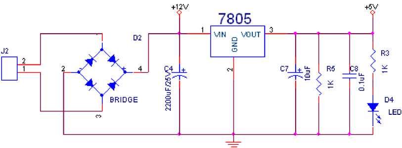
Fig. 1: Circuit diagram of power supply
A 230v, 50Hz Single phase AC power supply is given to a step down transformer to get 12v supply. This voltage is converted to DC voltage using a Bridge Rectifier. The converted pulsating DC voltage is filtered by a 2200uf capacitor and then given to 7805 voltage regulator to obtain constant 5v supply. This 5v supply is given to all the components in the circuit. A RC time constant circuit is added to discharge all the capacitors quickly. To ensure the power supply a LED is connected for indication purpose. [4]
-
V. Microcontrollers Used
The AT89S52 is a low-power, high-performance CMOS 8-bit microcontroller with 8K bytes of in-system programmable Flash memory [4]. The device is manufactured using Atmel’s high-density nonvolatile memory technology and is compatible with the Industry-standard 80C51 instruction set and pin out. The on-chip Flash allows the program memory to be reprogrammed in-system or by a conventional nonvolatile memory programmer. By combining a versatile 8-bit CPU with in-system programmable Flash on a monolithic chip, the Atmel AT89S52 is a powerful microcontroller which provides a highly-flexible and cost-effective solution to many embedded control applications. The AT89S52 provides the following standard features: 8K bytes of Flash, 256 bytes of RAM, 32 I/O lines, Watchdog timer, two data pointers, three 16-bit timer/counters, a six-vector two-level interrupt architecture, a full duplex serial port, on-chip oscillator, and clock circuitry [5]. In addition, the AT89S52 is designed with static logic for operation down to zero frequency and supports two software selectable power saving modes. The Idle Mode stops the CPU while allowing the RAM, timer/counters, serial port, and interrupt system to continue functioning. The Power down mode saves the RAM con-tents but freezes the oscillator, disabling all other chip functions until the next interrupt or hardware reset [5].
Features:
-
• Compatible with MCS®-51 Products
-
• 8K Bytes of In-System Programmable (ISP) Flash Memory –
Endurance: 1000 Write/Erase Cycles
-
• 4.0V to 5.5V Operating Range
-
• Fully Static Operation: 0 Hz to 33 MHz
-
• Three-level Program Memory Lock
-
• 256 x 8-bit Internal RAM
-
• 32 Programmable I/O Lines
-
• Three 16-bit Timer/Counters
-
• Eight Interrupt Sources
-
• Full Duplex UART Serial Channel
-
• Low-power Idle and Power-down Modes
-
• Interrupt Recovery from Power-down Mode
-
• Watchdog Timer
-
• Dual Data Pointer
-
• Power-off Flag
-
• Fast Programming Time
-
• Flexible ISP Programming (Byte and Page Mode)
-
• Green (Pb/Halide-free) Packaging Option
-
V I. ADC 0808 and 0809
-
The ADC0808, ADC0809 data acquisition component is a monolithic CMOS device with an 8-bit analog-to-digital converter, 8-channel multiplexer and microprocessor compatible control logic. The 8-bit A/D converter uses successive approximation as the conversion technique. The converter features a high impedance chopper stabilized comparator, a 256R voltage divider with analog switch tree and a successive approximation register. The 8-channel multiplexer can directly access any of 8-single-ended analog signals. The device eliminates the need for external zero and full-scale adjustments. Easy interfacing to microprocessors is provided by the latched and decoded multiplexer address inputs and latched TTL TRISTATE® outputs. The design of the ADC0808, ADC0809 has been optimized by incorporating the most desirable aspects of several A/D conversion techniques. The ADC0808, ADC0809 offers high speed, high accuracy, minimal temperature dependence, excellent long-term accuracy and repeatability, and consumes minimal power. These features make this device ideally suited to applications from process and machine control to consumer and automotive applications. The following are the summary of features:
-
• Easy interface to all microprocessors
-
• Operates ratio metrically or with 5 VDC or analog span
-
• Adjusted voltage reference
-
• No zero or full-scale adjust required
-
• 8-channel multiplexer with address logic
-
• 0V to 5V input range with single 5V power supply
-
• Outputs meet TTL voltage level specifications
-
• Standard hermetic or molded 28-pin DIP package
-
• 28-pin molded chip carrier package
-
• ADC0808 equivalent to MM74C949
-
• ADC0809 equivalent to MM74C949-1
-
VII. Max 232
The MAX232 is an integrated circuit that converts signals from an RS-232 serial port to signals suitable for use in TTL compatible digital logic circuits. The MAX232 is a dual driver/receiver and typically converts the RX, TX, CTS and RTS signals [6]. The drivers provide RS-232 voltage level outputs (approx. ± 7.5 V) from a single + 5 V supply via on-chip charge pumps and external capacitors. This makes it useful for implementing RS-232 in devices that otherwise do not need any voltages outside the 0 V to + 5 V range, as power supply design does not need to be made more complicated just for driving the RS-232 in this case. The receivers reduce RS-232 inputs (which may be as high as ± 25 V), to standard 5 V TTL levels. These receivers have a typical threshold of 1.3 V, and a typical hysteresis of 0.5 V. The later MAX232A is backwards compatible with the original MAX232 but may operate at higher baud rates and can use smaller external capacitors – 0.1 μF in place of the 1.0 μF capacitors used with the original device [6].
-
VIII. ZIGBEE
Zigbee is a specification for a suite of high level communication protocols using small, low-power digital radios based on the IEEE 802.15.4-2003 standard for wireless personal area networks (WPANs), such as wireless headphones connecting with cell phones via short-range radio. The technology defined by the Zigbee specification is intended to be simpler and less expensive than other WPANs, such as Bluetooth. Zigbee is targeted at radio-frequency (RF) applications that require a low data rate, long battery life, and secure networking. The features are summarized as follows.
-
• IEEE Std. 802.15.4™ Compliant RF Transceiver
-
• Supports Zigbee ® , MiWi™, MiWi™ P2P and
-
• Proprietary Wireless Networking Protocols
-
• Small Size: 0.7” x 1.1” (17.8 mm x 27.9 mm),
-
• Surface Mountable
-
• Integrated Crystal, Internal Voltage Regulator,
-
• Matching Circuitry and PCB Antenna
-
• Easy Integration into Final Product – Minimize
-
• Product Development, Quicker Time to Market
-
• Radio Regulation Certification for United States
-
• (FCC), Canada (IC) and Europe (ETSI)
-
• Compatible with Microchip Microcontroller
-
• Families (PIC16F, PIC18F, PIC24F/H, dsPIC33 and
PIC32)
-
• Up to 400 ft. Range
-
IX. Transmitter and Receiver Sections
Transmitter Section Block Diagram
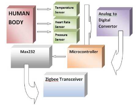
Fig. 2: Block diagram of Transmitter
Receiver Section Block Diagram

Fig. 3: Block diagram of Receiver
-
X. System Construction
The physiological information monitor system is designed and developed to perform the following functions. Measuring the bio signals of the patient and sending the data to the ADC is the main task here. The ADC converts the analog signals to digital signals which are compatible with the microcontroller. The microcontroller then sends the output signals to the max 232 which converts the data to the desired format which is computable by the PC .The max232 then serially transmits the data to a Zigbee transceiver. [7]
The microcontroller takes the role of a processor in the Zigbee network. The physiological information from each monitor device is sent to a PC of information server using RS-232 connected to a Zigbee transceiver. Physicians can monitor the patient’s physiological information with this information server. The patient’s health can be monitored and managed anytime and anywhere. The physiological information monitor device hardware are formed with Microchip’s Atmel 89S52;max 232;Zigbee transmitter and receiver. The monitor device has the PPG measure circuit and the control center has the RS-232 voltage level switching circuit.
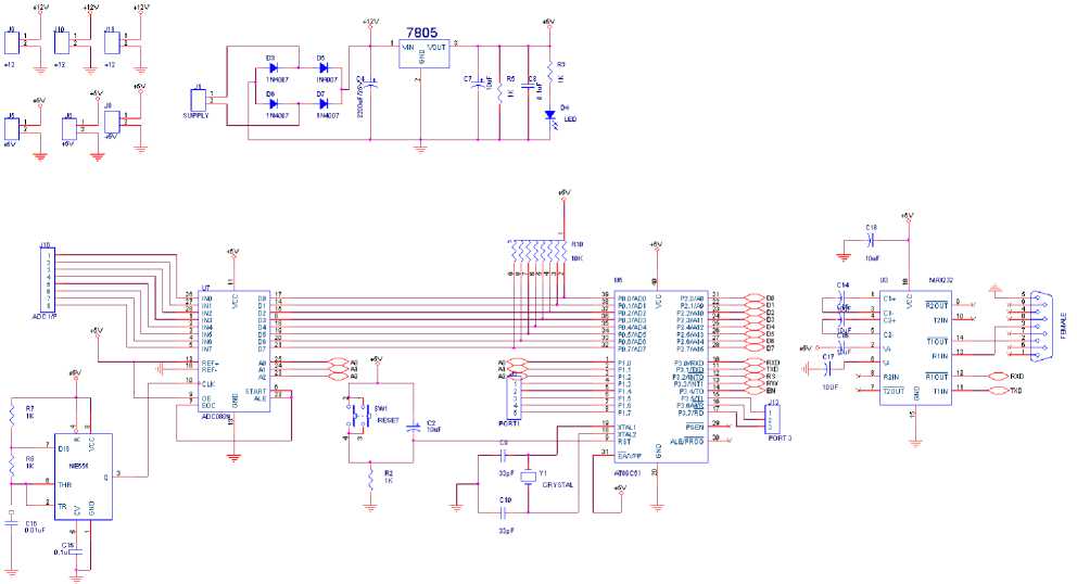
Fig. 4: Entire circuit diagram
In Hardware experiments, it’s usually quite hard to get the correct outputs so in order to get the results correct the most important part is to choose the most compatible circuit components among the available components in a very economic manner. Previously as mentioned in the literature survey we have given all the brief details needed for the components we have used in our paper. Now, we would like to mention each of the components needed to finish the paper. Three sensors are being used in this project and are listed as follows 1.Temperature sensor, 2. Pressure sensor and 3. Heart beat sensor. Each of these sensors produces a voltage corresponding to their physiological information, and then the sensors are connected to the J16 ADC input pin as shown in the circuit diagram. The ADC as its name suggests converts the Analog signal to the Digital signal [8]. The ADC0808 data acquisition component is a monolithic CMOS device with an 8-bit analog-to-digital converter, 8-channel multiplexer and microprocessor compatible control logic. The 8-bit A/D converter uses successive approximation as the conversion technique. The converter features a high impedance chopper stabilized comparator, a 256R voltage divider with analog switch tree and a successive approximation register. The 8-channel multiplexer can directly access any of 8-single-ended analog signals. The device eliminates the need for external zero and full-scale adjustments [8].
Now as we had mentioned the way we convert the Analog signals to Digital signals. We use a Microcontroller as the control center to co-ordinate every action of the sensors and the serial communication to the computers. The ADC output is connected to Port 0 of the microcontroller. Port 0 acts as an input when a high impedance external pull up is connected to it. The microcontroller which we use is an Atmel AT89S52. Here is a few lines about the microcontroller that we are going to use. The AT89S52 is a low-power, high-performance CMOS 8-bit microcontroller with 8K bytes of in-system programmable Flash memory. The device is manufactured using Atmel’s high-density nonvolatile memory technology and is compatible with the Industry-standard 80C51 instruction set and pin out. The on-chip Flash allows the program memory to be reprogrammed in-system or by a conventional nonvolatile memory programmer. By combining a versatile 8-bit CPU with in-system programmable Flash on a monolithic chip, the Atmel AT89S52 is a powerful microcontroller which provides a highly-flexible and cost-effective solution to many embedded control applications. The AT89S52 provides the following standard features: 8K bytes of Flash, 256 bytes of RAM, 32 I/O lines, Watchdog timer, two data pointers, three 16-bit timer/counters, a six-vector two-level interrupt architecture, a full duplex serial port, on-chip oscillator, and clock circuitry. In addition, the AT89S52 is designed with static logic for operation down to zero frequency and supports two software selectable power saving modes. The Idle Mode stops the CPU while allowing the RAM, timer/counters, serial port, and interrupt system to continue functioning. The Powerdown mode saves the RAM con-tents but freezes the oscillator, disabling all other chip functions until the next interrupt or hardware reset. Besides being of such flexible nature it has quite a few advantage features such as, 4.0V to 5.5V operating range, watchdog timer and 256x8 bit internal RAM etc.
Since we are using very sensitive devices we should know that the proper power supply is being fed to the components. This is done through passing the signals through extensive capacitors and filter circuits. A 230v, 50Hz Single phase AC power supply is given to a step down transformer to get 12v supply. This voltage is converted to DC voltage using a Bridge Rectifier. The converted pulsating DC voltage is filtered by a 2200uf capacitor and then given to 7805 voltage regulator to obtain constant 5v supply. This 5v supply is given to all the components in the circuit. A RC time constant circuit is added to discharge all the capacitors quickly. To ensure the power supply a LED is connected for indication purpose.
Now after configuring all the microcontroller parts we need to convert the output from the controller into voltage range of the computer so we use a UART A universal asynchronous receiver/transmitter is a type of "asynchronous receiver/transmitter", a piece of computer hardware that translates data between parallel and serial forms. UARTs are commonly used in conjunction with other communication standards such as EIA RS-232. A UART is usually an individual (or part of an) integrated circuit used for serial communications over a computer or peripheral device serial port. UARTs are now commonly included in microcontrollers. A dual UART or DUART combines two UARTs into a single chip. Many modern ICs now come with a UART that can also communicate synchronously; these devices are called USARTs. The Universal Asynchronous Receiver/Transmitter (UART) controller is the key component of the serial communications subsystem of a computer. The UART takes bytes of data and transmits the individual bits in a sequential fashion. At the destination, a second UART re-assembles the bits into complete bytes. Serial transmission of digital information (bits) through a single wire or other medium is much more cost effective than parallel transmission through multiple wires. A UART is used to convert the transmitted information between its sequential and parallel form at each end of the link. Each UART contains a shift register which is the fundamental method of conversion between serial and parallel forms. We are using the MAX-232 standard in this paper, The MAX232 is an integrated circuit that converts signals from an RS-232 serial port to signals suitable for use in TTL compatible digital logic circuits. The MAX232 is a dual driver/receiver and typically converts the RX, TX, CTS and RTS signals.
The drivers provide RS-232 voltage level outputs (approx. ± 7.5 V) from a single + 5 V supply via on-chip charge pumps and external capacitors. This makes it useful for implementing RS-232 in devices that otherwise do not need any voltages outside the 0 V to + 5 V range, as power supply design does not need to be made more complicated just for driving the RS-232 in this case.
The receivers reduce RS-232 inputs (which may be as high as ± 25 V), to standard 5 V TTL levels. These receivers have a typical threshold of 1.3 V, and a typical hysteresis of 0.5 V.
The later MAX232A is backwards compatible with the original MAX232 but may operate at higher baud rates and can use smaller external capacitors – 0.1 μF in place of the 1.0 μF capacitors used with the original device.
Now as we have already mentioned the basic working and the interfacing between each component, we would like to give information on the sensors that have been used for the paper. To start with the first sensor we would like to explain is the Temperature sensor. Several temperature sensing techniques are currently in widespread usage. The most common of these are RTDs, thermocouples, thermistors, and sensor ICs. The right one for your application depends on the required temperature range, linearity, accuracy, cost, features, and ease of designing the necessary support circuitry. In this section we discuss the characteristics of the most common temperature sensing techniques. Temperature sensor we used here is LM35. The LM35 series are precision integrated-circuit temperature sensors, whose output voltage is linearly proportional to the Celsius (Centigrade) temperature. The LM35 thus has an advantage over linear temperature sensors calibrated in ° Kelvin, as the user is not required to subtract a large constant voltage from its output to obtain convenient Centigrade scaling. The LM35 does not require any external calibration or trimming to provide typical accuracies. The LM35’s low output impedance, linear output, and precise inherent calibration make interfacing to readout or control circuitry especially easy. It can be used with single power supplies, or with plus and minus supplies. The LM35 series also has quite advantageous features such as it marked directly in Centigrade, low cost and can be used for remote applications.
The next sensor that we explain is the pressure sensor, Pressure sensors are used for control and monitoring in thousands of everyday applications. Pressure sensors can also be used to indirectly measure other variables such as fluid/gas flow, speed, water level, and altitude. Pressure sensors can alternatively be called pressure transducers, pressure transmitters, pressure senders, pressure indicators and piezometers, manometers, among other names.
The MPX5050/MPXV5050G series piezoresistive transducer is a state-of-the-art monolithic silicon pressure sensor designed for a wide range of applications, but particularly those employing a microcontroller or microprocessor with A/D inputs. This patented, single element transducer combines advanced micromachining techniques, thin-film metallization, and bipolar processing to provide an accurate, high level analog output signal that is proportional to the applied pressure.
The next sensor that is being used is the heartbeat sensor, This heart beat sensor is designed to give digital output of heat beat when a finger is placed inside it. When the heart detector is working, the top-most LED flashes in unison with each heart beat. This digital output can be connected to microcontroller directly to measure the Beats per Minute (BPM) rate. It works on the principle of light modulation by blood flow through finger at each pulse. The sensor consists of a super bright red LED and light detector. The LED needs to be super bright as the light must pass through finger and detected at other end. Now, when the heart pumps a pulse of blood through the blood vessels, the finger becomes slightly more opaque and so less light reached the detector. With each heart pulse the detector signal varies. This variation is converted to electrical pulse. The electrical pulse is then amplified and the apt voltage levels are generated. The output signal is also indicated on top by a LED which blinks on each heart beat.
As mentioned earlier one of the key features in our paper is, the physiological information values gathered by the sensors are wirelessly transmitted to a PC. This is done by using a wireless technology known as Zigbee. Zigbee is a specification for a suite of high level communication protocols using small, low-power digital radios based on the IEEE 802.15.4-2003 standard for wireless personal area networks (WPANs), such as wireless headphones connecting with cell phones via short-range radio. The technology defined by the Zigbee specification is intended to be simpler and less expensive than other WPANs, such as Bluetooth. Zigbee is targeted at radio-frequency (RF) applications that require a low data rate, long battery life, and secure networking.
As this is a hardware paper, the result of the completed paper can be demonstrated using the assembled kit and a PC. The result of the paper is that the temperature, heartbeat rate and the blood pressure readings are gathered and are sent to the PC wirelessly using Zigbee.
Receiver section
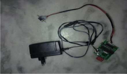
Fig. 5: Receiver part
Transmitter section
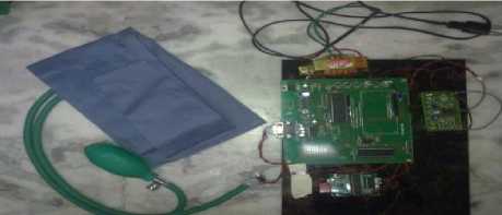
Fig. 6: Transmitter part
-
XI. Conclusion
This Paper has been successfully constructed with hardware and it demonstrates an automated patient monitoring system. Its merits and future prospectus are summarized below:
Merits
The wireless system is useful for monitoring the patient’s condition from a distance.
Measuring all the physiological information digitally is more accurate and the method is not time consuming.
The clinical information database contains all data regarding the patients in electronic form and can be used for future case studies.
Future Prospects
The sensors used in this paper are of inexpensive build quality and hence accuracy has to be kept in mind when we take this approach to build a highly sensitive system where a patient’s life is of great importance. In future, if we are going to build a same system with high accuracy sensors, then the system will be very much effective and possess excellent quality.
References Design and Development of an Embedded System for Monitoring the Health Status of a Patient
- Feng Zhao, Leonidas Guibas, Wireless Sensor Networks, 1st Edition Morgan Kaufmann publishers 2006.
- R.S.Khandpur, Handbook of Bio-Medical Instrumentation, 16th Edition Tata McGraw Hill Publishing Co.Ltd.2003.
- Jacob Fradin, Handbook of Modern sensors-Physics, Designs and Applications, 3rd edition, 2004, Springer Science + Business Media, Inc, USA.
- Morris Mano and Michael D. Ciletti, Digital Design, Pearson Education, 4th Edition, Indian version.
- Shriram K Vasudevan, D P Kothari, RMD Sundaram, Embedded systems, 2012 Edition, New age publications, New Delhi, India.
- Ramesh Goankar, Microprocessor Architecture, Programming and applications with 8085, Penram international publishing, Fifth edition, India.
- M. Saravanan, S. Jeevananthan, N. Senthil Kumar, Microprocessors and Microcontrollers, Oxford University Press India, 2010.
- Roy Chowdhury, Linear Integrated Circuits,12th reprint, Jaico Publishing House.
