Design and Implementation of Low Power 8-bit Carry-look Ahead Adder Using Static CMOS Logic and Adiabatic Logic

Author: Abdul Sajid, Ahmad Nafees, Saifur Rahman
Journal: International Journal of Information Technology and Computer Science(IJITCS) @ijitcs
Article in issue: 11 Vol. 5, 2013.
Free access
Addition forms the basic structure for many processing operations like counting, multiplication, filtering etc. Adder circuits that add two binary numbers are of great interest for many designers. The simplest approach to design an adder is to implement gates to yield the required logic function. Carry-look ahead adder is a major functional block in arithmetic logic unit due to its high speed operation. The arithmetic logic unit has been widely used in microprocessor systems and mostly in processing modules of embedded systems. Therefore, it is of interest to study the functional behavior and power consumption carry-look ahead adder. In this project, the adder is implemented using 180 nm CMOS technology on bulk substrate. Two logic families i.e. static CMOS and adiabatic logic have been analyzed and implemented to study the transient characteristics of the adder. Finally the power consumption is estimated and compared. From the results it has been found that the static CMOS logic offers low delay whereas the adiabatic logic consumes low power.
Adiabatic Logic, GATE, Power Analysis, CMOS
Short address: https://sciup.org/15011994
IDR: 15011994
Text of the scientific article Design and Implementation of Low Power 8-bit Carry-look Ahead Adder Using Static CMOS Logic and Adiabatic Logic
Published Online October 2013 in MECS
Binary addition is a popular methodology among computational logic elements. There are lots of ways of implementing the binary addition. Encoding, replication of common factors and pre-charging are some of them. Also the same functional block can be implemented using different logic approach like static, CMOS, dynamic logic, pass transistor based logic and adiabatic logic etc. Each method is having its own advantage based on simplicity, in terms of area that is related to cost, delay and power consumption. The n-bit adder has n one-bit full adders known as ripple carry adder. In this method the carry is computed. The addition is not complete until the n-1th adder has computed the n-1th output. The carry chain is meant for the total delay of the logic element. Therefore, speeding up the adder needs the speeding up the carry chain. As speed of the addition is the main criteria with nominal amount of power consumption, the carry look ahead adder has been chosen. The carry-look-ahead adder is one way to speed up the carry computation. The carry-look-ahead adder breaks the carry computation into two steps, starting with the computation of two intermediate values. If the adder has two inputs ai and bi, then Pi and Gi can be written as follows.
Pi = ai® bi(1)
Gi = ai" bi(2)
Using c i as the carry input, the sum and carry output can be written as follows.
S; = c (xor) az (xor) bz
Ci+i = Gi + PiCi(4)
Expanding the c i , the c i+1 can be generated as a function of inputs and c 0.
In this way the 8-bit carry-look ahead adder functional block diagram can be as follows. The functional block carries two 8-bit inputs and 7 carry outputs as shown in the figure 1. The Cin and 7 carry outputs have been used to generate 8-bit sum output. The logic function is implemented by two methods.
-
1. Static CMOS logic
-
2. Adiabatic CMOS logic
The delay and power consumtion of 8-bit CLA has been evaluated and compared.
-
II. Static CMOS Implementation
Gordon Moore predicted that integrated circuit density and performance would double every 18 months known as famous “Moore’s Law”. Si MOSFETs have demonstrated remarkable scaling over the past four decades [1-2]. The scaling of the MOS transistor plays the main driving force behind the rapid improvements in integrated circuit products with excellent performance [3]. These improved performance would come from reduced transistor dimensions, increased transistor counts, and increased operating frequencies. The important feature of scaled MOS transistors is the reduction in the amount of energy used during a switching event. Switching energy reduction is derived from the combination of lower parasitic capacitance from smaller feature sizes and from lower operating voltage. A metric for estimating MOS transistor switching energy is CV2. Where C is the transistor gate capacitance and V being the operating voltage. Transistor switching energy has become increasingly important due to overall circuit power constraints.
The CMOS complementary logic gates have two function determining blocks such as n-block and p-block. There are normally 2n number of transistors in an n input logic gate. The most important reason for using static CMOS logic is its low static power dissipation, due to the absence of dc currents during periods when no signal transients occur. However, during an edge of an input signal there will always be a short-circuit current flowing from supply to ground in static CMOS circuits.
To illustrate the fundamentals of logic circuits we will use the following circuit examples that are INVERTER, AND and XOR gate. The circuit diagrams and the simulation results of these elements are shown as follows. From the analysis of logic operations it can be shown that the tasks are basically charging and discharging of parasitic capacitances while propagating signals through various logic functions. Logic transistors need low input capacitance and high output conductance.
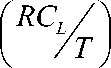
Therfore 1.8 V supply voltage has been used. In this work 180 nm channel length MOSFETs have ben used for simulation purposes. power consumption in CMOS circuits becomes increasingly important. Therefore, it is important to have a detailed understanding of the power consumption behavior of digital CMOS circuits. Off-state leakage is static power, current that leaks through transistors even when they are turned off. It is one of two principal sources of power dissipation in today’s microprocessors. The other is dynamic power, which arises from the repeated capacitance charge and discharge on the output of the hundreds of millions of gates in today’s chips. Until very recently, only dynamic power has been a significant source of power consumption, and Moore’s law has helped to control it. Shrinking processor technology has allowed and, below 100 nanometers, actually required reducing the supply voltage. Dynamic power is proportional to the square of supply voltage, so reducing the voltage significantly reduces power consumption. Five equations model the power-performance tradeoffs for CMOS logic circuits. We present them here in simplifications that capture the basics for logic CMOS designs. The following equation shows the dependency of operating frequency on supply voltage.
f «(V-Vh)"/V (5)
where V is the transistor’s supply voltage, V th is its threshold or switching voltage, and the exponent α is an experimentally derived constant that, for current technology, is approximately 1.3. The next equation defines overall power consumption as the sum of dynamic and static power.
P = ACV2 f + VI 1юк (6)
During the last five years CMOS technology has become one of the most dominant technologies for VLSI circuits. The most important reason for this is its low static power dissipation, due to the absence of dc currents during periods when no signal transients occur [4-5]. However, during an edge of an input signal there will always be a short-circuit current flowing from supply to ground in static CMOS circuits. So far only limited analyses and discussions have appeared in the literature on this power component of static CMOS circuits. In integrated circuits it is always necessary to drive large capacitances (bus lines, “off-chip” circuitry, etc.), often at high clock frequencies. Such driving circuits (buffers) will take a relatively large part of the total power consumption of the chip. It is clear that optimization of such circuits requires a different approach as compared to optimization of CMOS logic. These buffer circuits need extra attention to obtain minimum power dissipation. Therefore, a detailed discussion on power dissipation of a basic CMOS inverter will be given first.
-
III. Inverter
CMOS circuits are constructed in such a way that all PMOS transistors must have either an input from the voltage source or from another PMOS transistor. Similarly, all NMOS transistors must have either an input from ground or from another NMOS transistor. The composition of a PMOS transistor creates low resistance between its source and drain contacts when a low gate voltage is applied and high resistance when a high gate voltage is applied. On the other hand, the composition of an NMOS transistor creates high resistance between source and drain when a low gate voltage is applied and low resistance when a high gate voltage is applied. CMOS accomplishes current reduction by complementing every nMOSFET with a pMOSFET and connecting both gates and both drains together. A high voltage on the gates will cause the nMOSFET to conduct and the pMOSFET to not conduct while a low voltage on the gates causes the reverse. This arrangement greatly reduces power consumption and heat generation. However, during the switching time both MOSFETs conduct briefly as the gate voltage goes from one state to another. CMOS inverters (Complementary NOSFET Inverters) are some of the most widely used and adaptable MOSFET inverters used in chip design. They operate with very little power loss and at relatively high speed. Furthermore, the CMOS inverter has good logic buffer characteristics, in that, its noise margins in both low and high states are large. This short description of CMOS inverters gives a basic understanding of the how a CMOS inverter works. It will cover input/output characteristics, MOSFET states at different input voltages, and power losses due to electrical current. A CMOS inverter contains a PMOS and a NMOS transistor connected at the drain and gate terminals, a supply voltage VDD at the PMOS source terminal, and a ground connected at the NMOS source terminal, were IN is connected to the gate terminals and OUT is connected to the drain terminals.(See diagram). It is important to notice that the CMOS does not contain any resistors, which makes it more power efficient that a regular resistor-MOSFET inverter. As the voltage at the input of the CMOS device varies between 0 and 1.8 volts, the state of the NMOS and PMOS varies accordingly. If we model each transistor as a simple switch activated by IN, the inverter’s operations can be seen very easily. The CMOS inverter is an important circuit device that provides quick transition time, high buffer margins, and low power dissipation. All three of these are desired qualities in inverters for most circuit design. The schematic of the inverter diagram is shown in Figure 1.
vdd
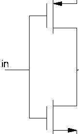
out
gnd
Fig. 1: Inverter schematic using static CMOS
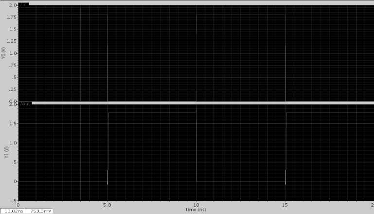
Fig. 2: Inverter output
-
IV. AND2
The CMOS NAND gate circuit may be used as the starting point for the creation of an AND gate. All that needs to be added is another stage of transistors to invert the output signal. In NAND gate, if both of the A and B inputs are high, then both the NMOS transistors (bottom half of the diagram) will conduct, neither of the PMOS transistors (top half) will conduct, and a conductive path will be established between the output and V ss (ground), bringing the output low. If either of the A or B inputs is low, one of the NMOS transistors will not conduct, one of the PMOS transistors will, and a conductive path will be established between the output and V dd (voltage source), bringing the output high.
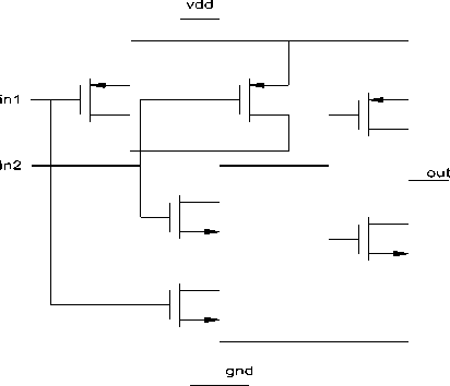
Fig. 3: AND gate schematic using static CMOS
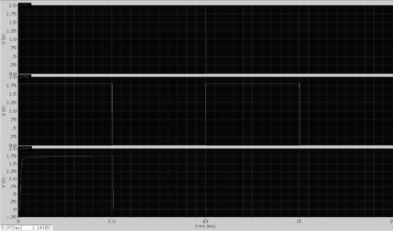
Fig. 4: AND gate results
-
V. XOR2:
The XOR gate is a digital logic gate that implements an exclusive OR; that is, a true output (1) results if one, and only one, of the inputs to the gate is true (1). If both inputs are false (0) or both are true (1), a false output (0) results. Its behavior is summarized in the truth table shown on the right. A way to remember XOR is "one or the other but not both". XOR represents the inequality function, i.e., the output is HIGH (1) if the inputs are not alike otherwise the output is LOW (0). XOR can also be viewed as addition modulo 2. As a result, XOR gates are used to implement binary addition in computers. The XOR logic gate can be used as a one-bit adder that adds any two bits together to output one bit. For example, if we add 1 plus 1 in binary, we expect a two-bit answer, 10 (i.e. 2 in decimal). Since the trailing sum bit in this output is achieved with XOR, the preceding carry bit is calculated with an AND gate. This is the main principle in half adders and the combined AND-XOR circuit may be chained together in order to add ever longer binary numbers.
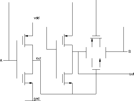
Fig. 5: XOR gate schematic
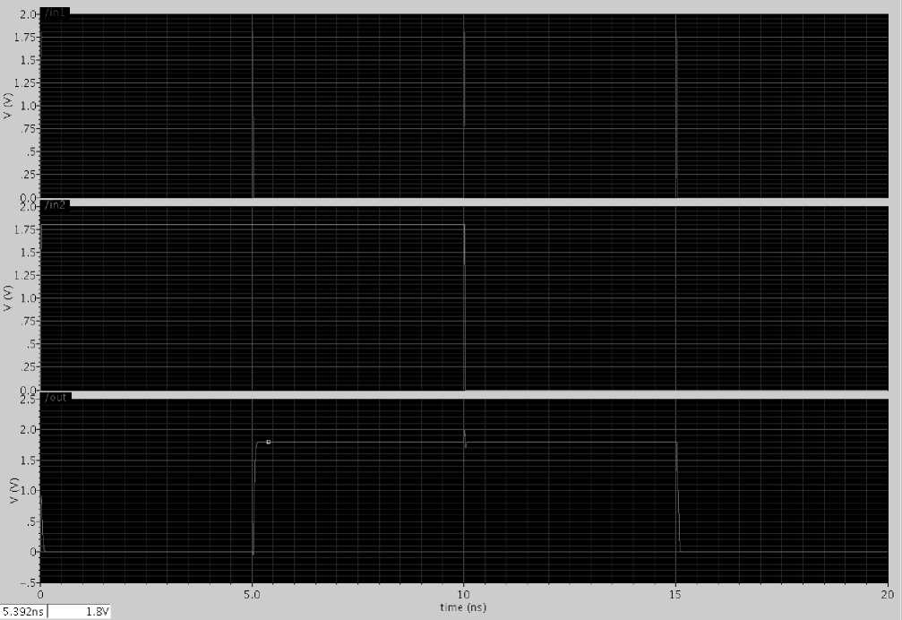
Fig. 6: XOR gate results
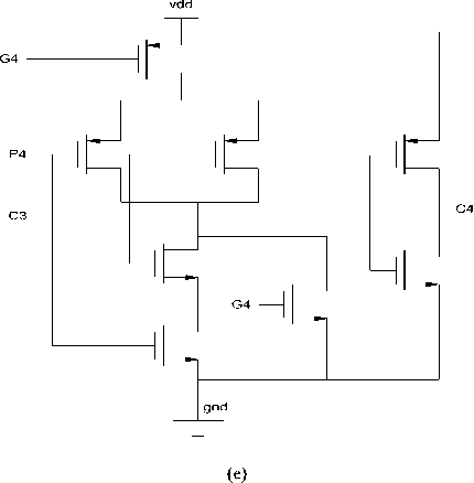
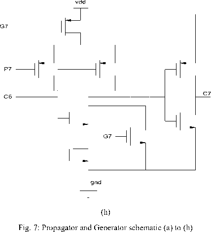
VI. Propagator and Generator:
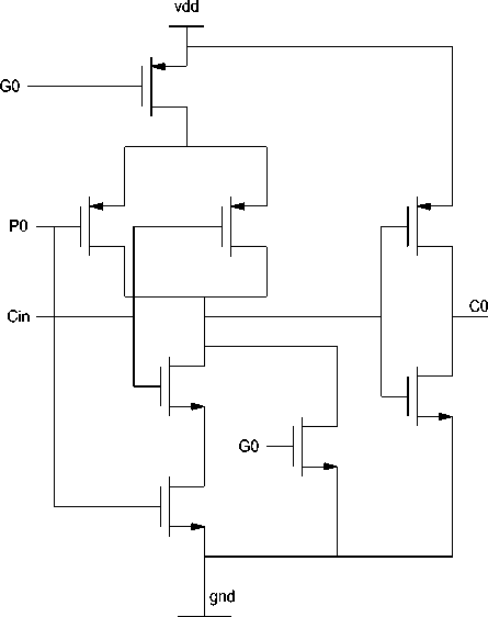
(a)
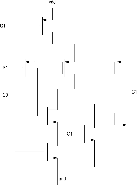
(b)
-
VII. 8 bit CLA:
Carry look ahead adder depends on two things that have been explained as follows.
-
1. Calculating, for each digit position, whether that position is going to propagate a carry if one comes in from the right.
-
2. Combining these calculated values to be able to deduce quickly whether, for each group of digits, that group is going to propagate a carry that comes in from the right.
Supposing that groups of 4 digits are chosen. Then the sequence of events goes something like this:
-
1. All 1-bit adders calculate their results.
-
2. Suppose that a carry arises in a particular group. Within at most 3 gate delays, that carry will emerge at the left-hand end of the group and start propagating through the group to its left.
-
3. If that carry is going to propagate all the way through the next group, the look ahead unit will already have deduced this. Accordingly, before the carry emerges from the next group the look ahead unit is immediately (within 1 gate delay) able to tell the next group to the left that it is going to receive a carry - and, at the same time, to tell the next look ahead unit to the left that a carry is on its way.
Simultaneously, the look ahead units perform their calculations.
The net effect is that the carries start by propagating slowly through each 4-bit group, just as in a ripple-carry system, but then move 4 times as fast, leaping from one look ahead carry unit to the next. Finally, within each group that receives a carry, the carry propagates slowly within the digits in that group. The more bits in a group, the more complex the look ahead carry logic becomes, and the more time is spent on the "slow roads" in each group rather than on the "fast road" between the groups (provided by the look ahead carry logic). On the other hand, the fewer bits there are in a group, the more groups have to be traversed to get from one end of a number to the other, and the less acceleration is obtained as a result. Deciding the group size to be governed by look ahead carry logic requires a detailed analysis of gate and propagation delays for the particular technology being used. It is possible to have more than one level of look ahead carry logic, and this is in fact usually done. Each look ahead carry unit already produces a signal saying "if a carry comes in from the right, I will propagate it to the left", and those signals can be combined so that each group of (let us say) four look ahead carry units becomes part of a "super group" governing a total of 16 bits of the numbers being added. The "super group" look ahead carry logic will be able to say whether a carry entering the super group will be propagated all the way through it, and using this information, it is able to propagate carries from right to left 16 times as fast as a naive ripple carry. With this kind of two-level implementation, a carry may first propagate through the "slow road" of individual adders, then, on reaching the left-hand end of its group, propagate through the "fast road" of 4-bit look ahead carry logic, then, on reaching the left-hand end of its super group, propagate through the "superfast road" of 16-bit look ahead carry logic. Again, the group sizes to be chosen depend on the exact details of how fast signals propagate within logic gates and from one logic gate to another. For very large numbers (hundreds or even thousands of bits) look ahead carry logic does not become any more complex, because more layers of super groups and super super groups can be added as necessary [6-8]. The increase in the number of gates is also moderate: if all the group sizes are 4, one would end up with one third as many look ahead carry units as there are adders. However, the "slow roads" on the way to the faster levels begin to impose a drag on the whole system (for instance, a 256-bit adder could have up to 24 gate delays in its carry processing), and the mere physical transmission of signals from one end of a long number to the other begins to be a problem. At these sizes carry-save adders are preferable, since they spend no time on carry propagation at all. Carry look ahead logic uses the concepts of generating and propagating carries. Although in the context of a carry look ahead adder [9-10], it is most natural to think of generating and propagating in the context of binary addition, the concepts can be used more generally than this. In the descriptions below, the word digit can be replaced by bit when referring to binary addition.
The addition of two 1-digit inputs A and B is said to generate if the addition will always carry, regardless of whether there is an input carry (equivalently, regardless of whether any less significant digits in the sum carry) [11]. For example, in the decimal addition 52 + 67, the addition of the tens digits 5 and
-
6 generates because the result carries to the hundreds digit regardless of whether the ones digit carries (in the example, the ones digit does not carry (2+7=9)). We chose the static carry-look ahead adder for a number of reasons based on a balance between size and speed. The fastest design implements a parallel structure, where each bit is calculated simultaneously. We were unable to utilize this design because of our chip real estate limitations. On the other hand, a serial adder is characterized by one of the simplest transistor structures, but is excruciatingly slow. We then examined the carrylook ahead adder, which is faster than the serial adder because the carry bit is calculated parallel to the XOR operation on the inputs bits. We had the option of going with a dynamic carry structure or a static structure.
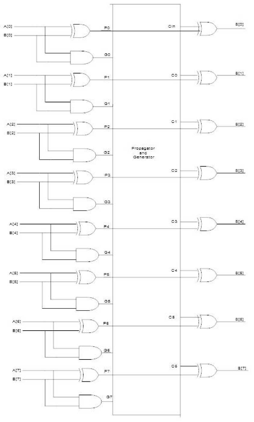
Fig. 8: 8 bit ca rry look ahead adder schematic
Delay of 8bit CLA with static CMOS logic:
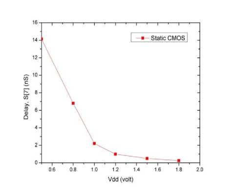
Fig. 9: 8 bit carry look ahead adder delay Power dissipation of 8bit CLA with static CMOS logic:
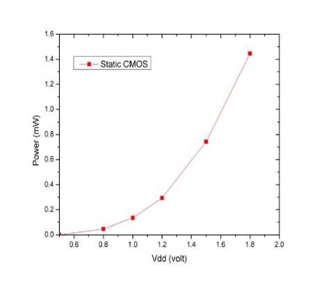
Fig. 10: 8 bit carry look ahead adder power consumption
-
VIII. Adiabatic Logic Implementation
Е =
DISS
L DD
Theoretically, it is possible to reduce the power dissipation by extending the switching time.The proposed circuit is the first ever 1-bit full adder based on two-phase clocked adiabatic logic to scale the power consumption down straightway with large number of applications in low power VLSI regime till date. A comparison of the same with standard CMOS is necessary.
An enormous amount of power is dissipated in high performance applications. Thus, the major deliberation needed in the design of VLSI circuits and systems, while using deep submicron technologies is the design for low power. The focus of circuit design has been towards the search for innovative unconventional low power design techniques. The adiabatic or energy recovery design is a novel circuit design method envisaged in this direction, which operates with minimum power dissipation and tolerable circuit complexity. They reclaim full or partial energy stored in the nodal capacitances and recycle them. They are classified into (1) fully adiabatic and (2) quasi-adiabatic circuits. While the former has no nonadiabatic loss realized at the expense of higher circuit density, the latter incurs some non-adiabatic loss with simpler circuit style. Navigating the current through devices with small potential difference and realizing efficient charge recovery from the nodal capacitances makes this possible. A number of quasi-adiabatic logic circuits consisting of the basic 2P or 2N2P latch operating at few hundreds of megahertz frequencies have been presented. Of these, the Positive Feedback Adiabatic Logic exhibits the lowest power consumption. It was also proved for its robustness. However, it suffers from energy loss due to the residual charge on the output nodes. This occurs when the output node is left floating during the time when the power-clock voltage is lower than the threshold voltage of the devices in the charging/discharging path. These circuits, primarily being differential circuits, incur the energy loss due to the floating complementary output nodes. The resulting vulnerability for current leakage and charge sharing proves to be a major impediment for their favored use at high frequencies also. Secondly, the sizing and number of transistors connected at the output nodes directly control the energy consumed by (1) mainly determining the load capacitance, (2) providing leakage paths and (3) chargesharing. The asymmetric and skewed logic gates favor one of the complementary nodes over the other. They make one of the outputs require less logical effort than the other. Some logic designs reduces the logic effort along the critical path by unequal transistor sizes. This results in varying node capacitance values, and the desired response of the rising/falling outputs is maneuvered, while aiming for reduced power. This asymmetric feature is exploited in the design of Asymmetric Positive Feedback Adiabatic Logic. Time often plays an important role in signal processing systems. Obviously, increasing the clock frequency is one way to improve the throughput, but adiabatic circuits cannot be clocked at very high frequencies. The maximum frequency of operation realized by an adiabatic circuit depends upon the efficiency of the Evaluation and Recovery phases. Power dissipation has become a prime constraint in high performance applications, especially in portable and battery operated ASIC systems. With technology scaling, the impact of power dissipation is expected to gain significance. The classical approaches to achieve low-power design are to reduce the supply voltage, the loading capacitances of gates and switching activity. However, these methods have several challenges with the shrink of CMOS technology sizes such as degraded voltage margin, increased leakage currents, and increased soft error rates. Adiabatic logic is a promising alternative low-power approach by utilizing AC voltage supplies (power-clocks) to recycle the energy of circuits instead of being dissipated as heat. Since dynamic power and energy are quadratically proportional to the supply voltage, the ability to operate at low voltages would further decrease dynamic energy dissipation. However, in the low-voltage regime, there will be an observable increase in static energy dissipation. Adiabatic logic developed in the past to operate at higher supply voltages do not necessarily operate as efficiently or at all at lower voltages.
-
IX. AND2:
The simulation results are shown in Figure 17 and Figure 18 where the energy advantages of adiabatic circuits over static CMOS counterparts can be seen. However, compormise has been done in the delay of the circuit.
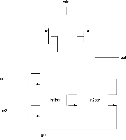
Fig. 11: Schematic of AND gate using adiabatic logic
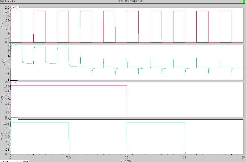
Fig. 12: Results of AND gate using adiabatic logic Xor2
vdd
in2bar
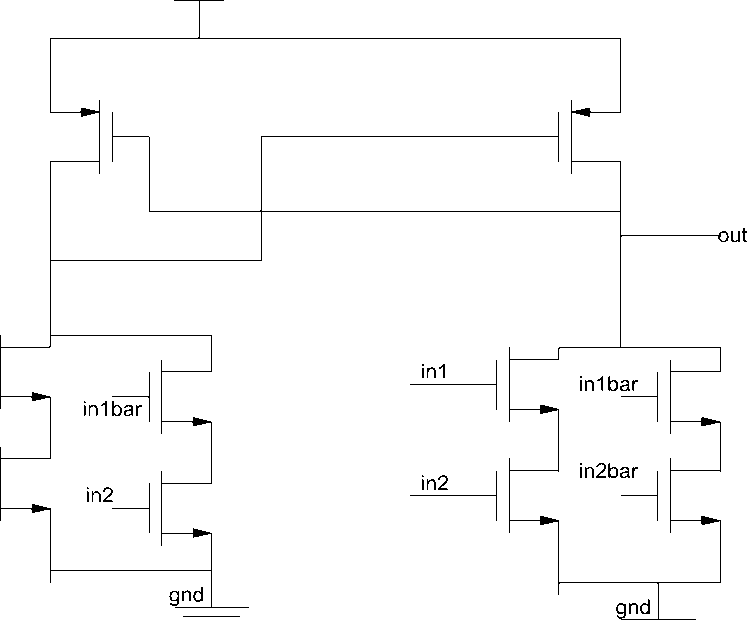
Fig. 13: Schematic of XOR gate using adiabatic logic
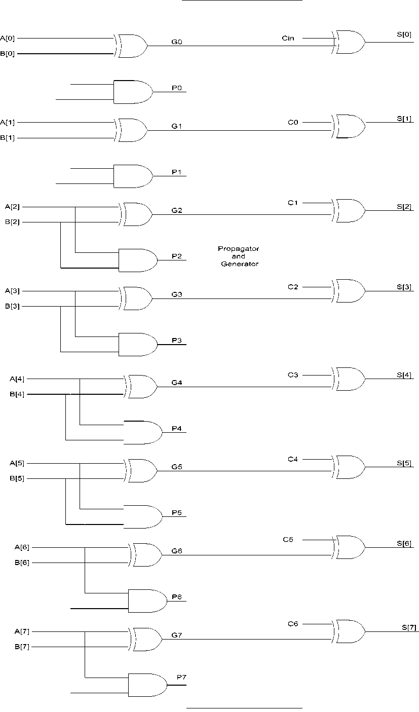
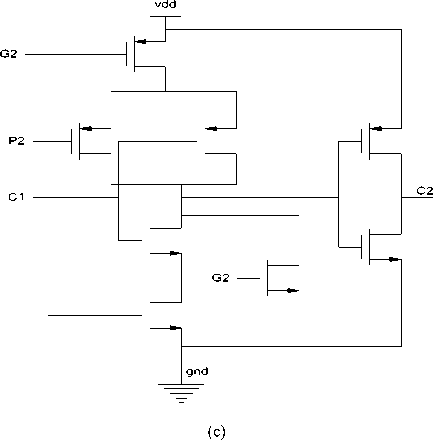
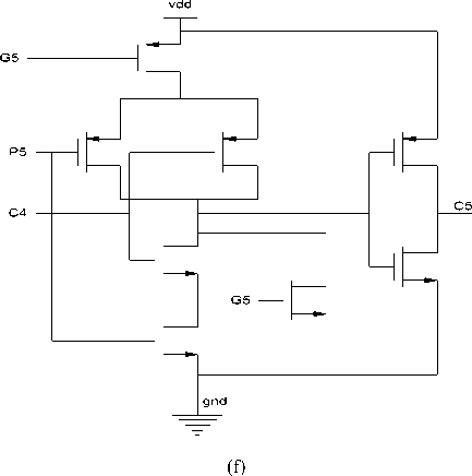
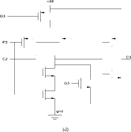
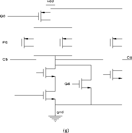
Fig. 15: Schematic of propagator and generator using adiabatic logic
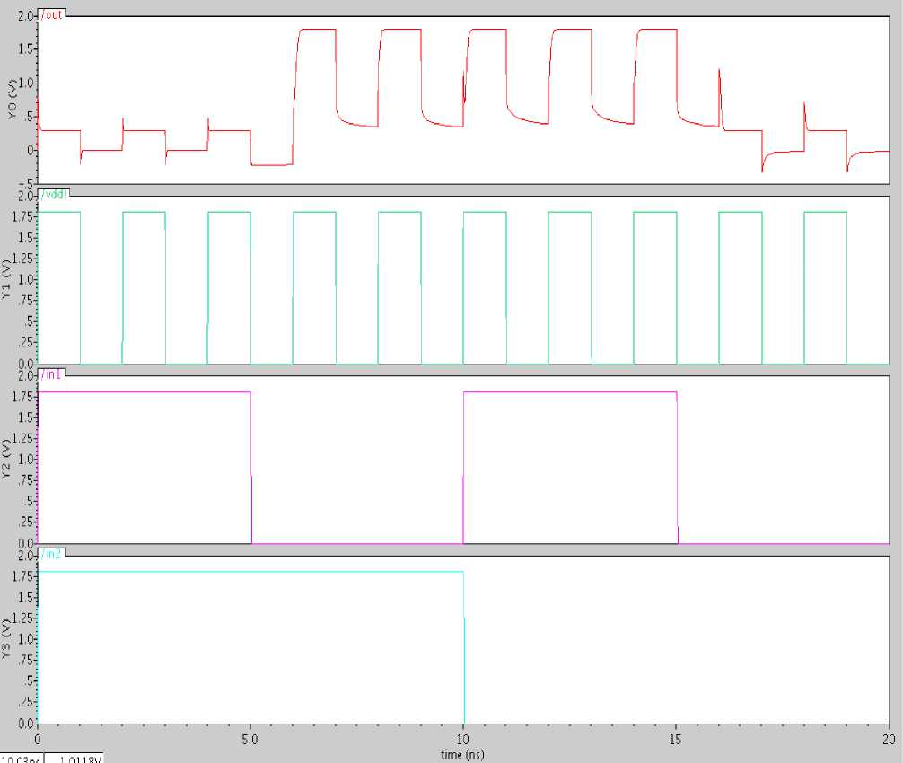
Fig. 14: Results of XOR gate using adiabatic logic 8 bit CLA
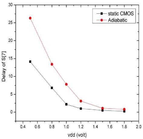
Fig. 16: Comparison of delay of 8 bit CLA
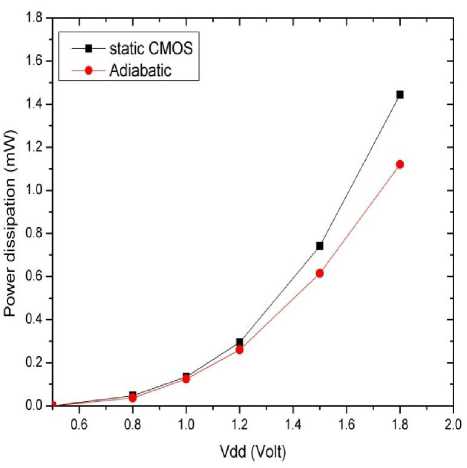
Fig. 17: Comparison of power consumption of 8 bit CLA
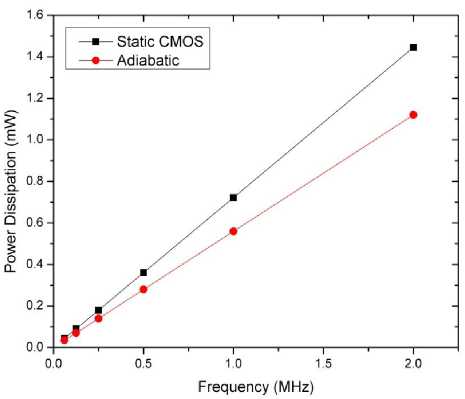
Fig. 18: Comparison of power consumption of 8 bit CLA by varying frequency
-
X. Conclusion
This work proposes an energy efficient adiabatic logic technique that would reduce the power consumption. This work also explores the design of ultra low-power adiabatic CMOS circuits. Optimization has been done in the complementary functional blocks for efficient power and frequency performance characteristics. The main idea behind adiabatic design is to transfer charge between circuit capacitances and a time varying power-clock source. This scheme enables the charge transfers to occur in a controlled manner, limiting the currents and thus decrease the energy dissipation across the active devices. The simulation results shows that the adiabatic 8-bit carry look ahead adder circuit consume very low power.
-
[1] M. I. Elmasry, “Digital MOS integrated circuits: A tutorial;’ Digital MOS Integrated Circuits. New York: IEEE Press pp. 4-27.
-
[2] A. Kapuma,” CMOS circuit optimization,” SolidState Electronics, vol. 26, no. 1, pp: 47-58, 1983.
-
[3] C. Mead and L. Conway, Introduction to VLSI Systems. New York: pp. 12-15.
-
[4] I. S. Abu-Khater, R H Yan, A. Bellaouar and M. I. Elmayry, “A 1- V low-power high-performance 32-bit conditional sum adder,” in 19% IEEE Symposium on Low Power Electronics, Oct 10-12, 1994, San Diego. pp 66-67.
-
[5] I. S. Abu-Khater, A Bellaouar, M. I. Elmasry, and R Yan, “Circuit/architecture for low-power high-perrormance 32bit adder.” in IEEE sponsored 5th Great Lakes VLSI Symposium, Buffalo, New York, March 1995, pp. 74-77.
-
[6] K. Yano, et al., “A 3.8-ns CMOS 16×16-b multiplier using complementary pass-transistor logic,” IEEE Journal of Solid State Circuits, vol. 25, no. 2, pp. 388-395, April 1990.
-
[7] J. M. Rabaey, A. Chandrakasan, and B. Nikolic, Digital Integrated Circuits: A Design Perspective, Prentice-Hall, 2nd ed., 2003.
-
[8] D. Radhakrishnan, “Low-voltage low-power CMOS full adder,” IEE Proceedings: Circuits, Devices and Systems, vol. 148, no. 1, pp. 19-24, Feb. 2001.
-
[9] S. Goel, A. Kumar, and M. A. Bayoumi, “Design of Robust, Energy-Efficient Full Adders for DeepSubmicrometer Design Using Hybrid-CMOS Logic Style,” IEEE Trans. On Very Large Scale Integration (VLSI) Systems, vol. 14, no. 12, pp. 1309-1321, Dec. 2006.
-
[10] R. Zimmermann and W. Fichtner, “Low-power logic styles: CMOS versus pass-transistor logic,” IEEE Journal of SolidState Circuits, vol. 32, no. 7, pp. 1079-1090, July 1997.
-
[11] M. Alioto and G. Palumbo, “Analysis and comparison on full adder block in submicron technology,” IEEE Trans. on Very Large Scale Integration (VLSI) Systems, vol. 10, no. 6, pp. 806-823, Dec. 2002.
-
[12] Guoqiang Hang, “Adiabatic CMOS Gate and Adiabatic Circuit Design for Low-Power Applications,” Design Automation Conference, 2005, pp. 803-808.
-
[13] W.C. Athas and L.J. Svensson, “Reversible Logic Issues in Adiabatic CMOS,” Physics and
Computation, 1994, Proceedings, pp. 111-118.
Results,” Low Power Electronics and Design, 1997, pp. 323 – 327.
-
[15] Jose C. Garcia, and Juan A. Montiel–Nelson and Saeid Nooshabadi, “A CMOS Adiabatic Inverter Operating with a Single Clock Power Supply to Reduce Non–Adiabatic Loss,” IEEE Asia Pacific conference on Circuits and Systems, APCCAS 2008, pp. 968 – 971.
-
[16] Dragan Maksimovic´, Vojin G. Oklobdžija, Borivoje Nikolic, and K. Wayne Current, “Clocked CMOS Adiabatic Logic with Integrated SinglePhase Power-Clock Supply,” SoC Design Conference, 2008, pp. 350-353.
-
[17] Ettore Amirante , Jiirgen Fischer, M a r h s Lang , Agnese Bargagli-Stoffi , Jorg Berthold, Christoph Heer, and Dons Schmitt-Landsiedel, “An Ultra Low-Power Adiabatic Adder Embedded in a
Standard 0.13pm CMOS Environment,” Solid State Circuits Conference, 2003 , pp. 599 - 602.
-
[18] Hee-sup Song and Jin-ku Kang, “A CMOS Adiabatic Logic for Low Power Circuit Design,” 2004 IEEE Asia-Pacific Conference on Advanced System Integrated Circuits 2004, pp. 348-351.
-
[19] Nazrul Anuar, Yasuhiro Takahashi and Toshikazu Sekine, “Two Phase Clocked Adiabatic Static CMOS Logic,” International symposium on System-on-Chip, 2009, pp. 83-86.
Mr. Abdul Sajid received B.Tech. degree in Electronics and Communication from U.P. Technical University, U.P, India, in 2006. He is pursuing his M.Tech.( thesis work) in Electronic Circuits& System at Integral University. Currently, he is Assistant Professor & Head of Electronic & Communication Engineering, Department in LIT, Lucknow, India. His research interest includes computer Architecture, VLSI design and microprocessor.
Mr. Ahmad Nafees received M.S. degree in Communication Engineering from York University, U.K. in 2011 and B.Tech degree in Electronics & Communication Engineering from Integral University in 2009. Currently, he is Assistant Professor, Department of E&C Engineering, Integral University, Lucknow, India. His research interest includes wireless communication.
Mr. Saifur Rahman received M.Tech degree in Electronic Circuits & System from Integral University in 2008 and B.Tech degree in Electronics & Communication Engineering from U.P. Technical University in 2005. Currently, he is Junior Associate Professor, Department of E&C Engineering, Integral University, and Lucknow, India. His research interest includes VLSI.
References Design and Implementation of Low Power 8-bit Carry-look Ahead Adder Using Static CMOS Logic and Adiabatic Logic
- M. I. Elmasry, “Digital MOS integrated circuits: A tutorial;’ Digital MOS Integrated Circuits. New York: IEEE Press pp. 4-27.
- A. Kapuma,” CMOS circuit optimization,” Solid-State Electronics, vol. 26, no. 1, pp: 47-58, 1983.
- C. Mead and L. Conway, Introduction to VLSI Systems. New York: pp. 12-15.
- I. S. Abu-Khater, R H Yan, A. Bellaouar and M. I. Elmayry, “A 1- V low-power high-performance 32-bit conditional sum adder,” in 19% IEEE Symposium on Low Power Electronics, Oct 10-12, 1994, San Diego. pp 66-67.
- I. S. Abu-Khater, A Bellaouar, M. I. Elmasry, and R Yan, “Circuit/architecture for low-power high-perrormance 32bit adder.” in IEEE sponsored 5th Great Lakes VLSI Symposium, Buffalo, New York, March 1995, pp. 74-77.
- K. Yano, et al., “A 3.8-ns CMOS 16×16-b multiplier using complementary pass-transistor logic,” IEEE Journal of Solid State Circuits, vol. 25, no. 2, pp. 388-395, April 1990.
- J. M. Rabaey, A. Chandrakasan, and B. Nikolic, Digital Integrated Circuits: A Design Perspective, Prentice-Hall, 2nd ed., 2003.
- D. Radhakrishnan, “Low-voltage low-power CMOS full adder,” IEE Proceedings: Circuits, Devices and Systems, vol. 148, no. 1, pp. 19-24, Feb. 2001.
- S. Goel, A. Kumar, and M. A. Bayoumi, “Design of Robust, Energy-Efficient Full Adders for Deep-Submicrometer Design Using Hybrid-CMOS Logic Style,” IEEE Trans. On Very Large Scale Integration (VLSI) Systems, vol. 14, no. 12, pp. 1309-1321, Dec. 2006.
- R. Zimmermann and W. Fichtner, “Low-power logic styles: CMOS versus pass-transistor logic,” IEEE Journal of SolidState Circuits, vol. 32, no. 7, pp. 1079-1090, July 1997.
- M. Alioto and G. Palumbo, “Analysis and comparison on full adder block in submicron technology,” IEEE Trans. on Very Large Scale Integration (VLSI) Systems, vol. 10, no. 6, pp. 806-823, Dec. 2002.
- Guoqiang Hang, “Adiabatic CMOS Gate and Adiabatic Circuit Design for Low-Power Applications,” Design Automation Conference, 2005, pp. 803-808.
- W.C. Athas and L.J. Svensson, “Reversible Logic Issues in Adiabatic CMOS,” Physics and Computation, 1994, Proceedings, pp. 111-118.
- Dragan Maksimovic, Vojin G. Oklobdiija, Borivoje Nikolic, K. Wayne Current, “Clocked CMOS Adiabatic Logic with Integrated Single-phase Power-Clock Supply: Experimental Results,” Low Power Electronics and Design, 1997, pp. 323 – 327.
- Jose C. Garcia, and Juan A. Montiel–Nelson and Saeid Nooshabadi, “A CMOS Adiabatic Inverter Operating with a Single Clock Power Supply to Reduce Non–Adiabatic Loss,” IEEE Asia Pacific conference on Circuits and Systems, APCCAS 2008, pp. 968 – 971.
- Dragan Maksimovic´, Vojin G. Oklobdžija, Borivoje Nikolic, and K. Wayne Current, “Clocked CMOS Adiabatic Logic with Integrated Single-Phase Power-Clock Supply,” SoC Design Conference, 2008, pp. 350-353.
- Ettore Amirante , Jiirgen Fischer, M a r h s Lang , Agnese Bargagli-Stoffi , Jorg Berthold, Christoph Heer, and Dons Schmitt-Landsiedel, “An Ultra Low-Power Adiabatic Adder Embedded in a Standard 0.13pm CMOS Environment,” Solid-State Circuits Conference, 2003, pp. 599 - 602.
- Hee-sup Song and Jin-ku Kang, “A CMOS Adiabatic Logic for Low Power Circuit Design,” 2004 IEEE Asia-Pacific Conference on Advanced System Integrated Circuits 2004, pp. 348-351.
- Nazrul Anuar, Yasuhiro Takahashi and Toshikazu Sekine, “Two Phase Clocked Adiabatic Static CMOS Logic,” International symposium on System-on-Chip, 2009, pp. 83-86.
