Design and Implementation of Multi Player Pong Game using Altera DE2 Board

Author: Tonmoy Saha, A. K. Tasfique Ahmed, S. M. Shamsul Alam
Journal: International Journal of Intelligent Systems and Applications @ijisa
Article in issue: 6 vol.15, 2023.
Free access
Pong game is a simple but entertaining game of logic control. This research paper presents the design and implementation of an FPGA-based Pong game that runs on an Altera DE2 board using Verilog HDL. This article explains the VGA controller, object creation and animation, and text subsystem and of course how to link them all together to build a functioning circuit. There is an interesting multi-player mode and single-player mode feature in this design scheme. This game's multiplayer mode features both real-time and automatic players to create a competitive atmosphere. This design method followed less complicated, fastest processing, and utilized memory requirements and logic elements. The single-player mode uses 1.3% of total logic elements, the two-player mode uses 1.32%, and automatic player vs. real player uses 1.456% of total logic elements which is very small compared to the other gaming schemes and it reduces the processing time that is cost-effective for universal use. All the modules are designed by using Verilog HDL. The synthesis is done with the help of Altera DE2 FPGA. Functional simulation and synthesis prove that the design is universally usable and combines different modules in one module that presents sound entertainment and extends the electronics application-based work in the future.
Video Graphics Array (VGA), Field Programmable Gate Array (FPGA), Algorithmic State Machine Diagram (ASMD), Read Only Memory (ROM), Finite State Machine (FSM), Register Transfer Logic (RTL), Red Green Blue (RGB)
Short address: https://sciup.org/15019018
IDR: 15019018 | DOI: 10.5815/ijisa.2023.06.03
Text of the scientific article Design and Implementation of Multi Player Pong Game using Altera DE2 Board
Computer and information technology have progressed significantly in recent years. Gaming is one of the computer applications that are essential to human relaxation and reducing stress. In the present time, many handheldbased games are becoming crazier and more popular. FPGA is an electronic device that is suitable for gaming applications. FPGA-based gaming opens up many possibilities like efficient, parallel processing, and reusability. It develops gaming specialist device which has reduced smartphone addiction in children. A concept for a "Multiplayer PONG game" based on FPGA is aimed at providing fun for individuals of all ages and serving as a superb resource for studying application-based electronics technology. Pong is chosen as a learning tool because it offers a chance to learn about FPGA, graphics, video games, and device drivers. In this game development scheme, we choose a top-down methodology for game implementation which reduces the cost and makes faster video processing and less memory requirement. This game is for entertainment but it is a combined application of electronic hardware and software application. It is the basic study of gaming chip design.
This design is all about completely running an FSMD with a minimum requirement of memory and less processing time. First of all, synchronization of work with the game display. The video graphics array (VGA) screen is synchronized by horizontal synchronization and vertical synchronization of lines and pixels. After synchronizing the display, the color of the display pixel needs to be fixed. 24’bit RGB output generates the display color. Graphics generation is another major part of the game. There are various types of graphics generation schemes, but there are several complexities to choosing the most efficient scheme. The game is all about change of display pixel color and this is called object animation. There is an automatic controlled opponent which makes the game more impressive. This opponent played like a real opponent and it created a competitive environment. When we think about the competitive environment, there are also some rules, scores, and lifetime of the game, and text subsystems implemented by the character generation circuit. Score and lifetime are counted by the two different counters. This total system needs a driver that controls the game and it's called the game controller which represents as ASMD of the game.
The work aims at establishing an interaction between the VGA controller, object creation, animation, text subsystem, and demonstrating different aspects of electronic instrument-based entertainment medium. There is a major issue about creating object generation without using SRAM and it is successfully generating an object. Object generation is like a framework that generates an object by the logical control of Altera DE2. A text generation circuit is also used here for showing text without any predetermined memory access. Text is displayed by mapping the display pixel. It can be used for all languages by changing the pixel mapping. It is the basic study of gaming chip design. In the previous study, we found that there is a single-player mood pong game. In this study, we have created a multi-player pong game to make a more competitive gaming environment. The most attractive feature of the game is the virtual player vs. real player, which draws people's attention even more. This article provides the numerical comparison and memory requirement of different schemes that help in FPGA-based design in the future. Memoryless and few logical elements consume less power and shorten the processing time for game processors. This work will take the Electronics technology one step ahead for future scientific research.
This paper's overview is as follows. Section 2 covers previous related work about the sector. Section 3 presented as the backbone of the work which introduces us to VGA display synchronization, display clock synchronization, display scan, color signal generation, object generation different schemes and its memory requirements, automatic opponent creation, object animation according to an external command, text generation and the making of a complete ASMD. Section 4 discusses about signal and workflow of the implementation, software simulation output, and numerical comparison between the gaming mode of the process. Section 5 is the concluding part that indicates the successful implementation and what can be extended in a future study about this sector.
2. Related Works
P.P. Chu provides comprehensive details about Video Graphics Array ( VGA ) synchronization. There is also a graphic generation with an object-mapped scheme described in his book. There are also details on animated objects, tile-mapped pixel generation, and full-screen text display. In addition to designing a top-level control Finite State Machine ( FSM ) that unifies the graphic and text subsystems and coordinates the overall circuit operation, the author adds a text interface for displaying scores and messages of the pong game [1]. Nagarjuna et al. have proposed a solution to implement a VGA controller on FPGA with an emphasis on creating motion-capable geometric shapes by using a Finite State Machine ( FSM ) . They claim that almost every video adapter on the market supports this design's display capabilities, which can be expanded up to 1368 x 768. The usage of FILE OUT operations is a good approximation, which eliminates the need for storage devices like First in First Out (FIFO) and is more cost-effective [2]. Ying et al. demonstrated a display controller implementation on an Altera FPGA with a focus on timing signal simulation. The portability that can be achieved by having the timing logic implemented in abstract hardware description languages was also emphasized in this paper. The advantages in processing effectiveness, optimized resource utilization, and extremely low power consumption were demonstrated by the results [3]. Kannadasan et al. highlighted the benefits that can be gained from FPGA and VHDL-based approaches, which allow us to create high-resolution displays with very little storage requirement or environmental footprint. These techniques can be used to address issues with insufficient bandwidth. Real-world applications serve as excellent examples of how to use a software library for handling text [4]. Pokharel et al. have proposed optimized drivers for PS/2 keyboard and VGA interface using HDL. Xilinx Virtex-II Pro is used to synthesize and implement the design. The mapped signals on the FPGA Board have been optimized to reduce resource usage. A VGA monitor and a PS/2 keyboard are used to implement the entire design in hardware [5]. The author demonstrates the effective use of FPGA in creating a VGA Controller. He also describes the timing function and top layer module design in this paper. They adopt the integration tools in addition to the programming methodology. Each module can be downloaded into an FPGA after receiving a compile, function simulation, layout simulation, and timing simulation. The circuit board's size can be significantly decreased using this technique, which can also increase system reliability and design flexibility. It can therefore significantly lower system costs [6]. Hong-bin et al. have designed the hardware interface circuit for the VGA display with FPGA and talked about the timing of the VGA display. VGA transmits real-time video image data that has been processed by the graphics card for display on the screen. Traditional microprocessors are unable to implement the VGA interface timing. FPGA can be used to create VGA interface drivers due to its high speed, parallel processing, and programmability [7]. This document aims to print characters by offering interfaces for connecting a VGA port for graphical output and a PS/2 port for keyboard input.
Then, this system will be synthesized on an FPGA board, and it should be able to run a program to display characters that accept keyboard input and output the results to a VGA monitor. Software development primarily consists of two components, both of which are based on the Spartan 3E Starter Board Hardware Architecture: the PS/2 keyboard scan code receiving and processing program and the VGA displaying program [8]. The author suggested using VHDL as a logical language to describe the design of a resource-saving string display module and a high-resolution VGA control module. There are many designs for FPGA-based VGA controllers, but there are still major gaps like low-resolution displays and Chinese characters display modules using up a lot of resources. He also provided two main modules for designing concepts and logic diagrams. Experiments also reveal that while Chinese characters guarantee a high-resolution display, the display's need for storage resources significantly decreased [9]. Nguyen et al. presented The Duck Hunt Game on an FPGA prototyping board, specifically the Spartan 3 FPGA Prototyping Board. This project aims to develop an FPGA video game by combining digital design and UML. Verilog Hardware Description Language is used to implement the FPGA game. The author’s goal is to demonstrate the differences between FPGA and software video game development [10]. This article provides a programming design using VHDL for a Tetris game based on an FPGA. The PS/2 interface keyboard allows game players to move and rotate blocks, and a VGA monitor displays the game's video. The game figured out how to move and rotate the blocks, generate new blocks at random, get rid of rows, get points, and accelerate. The VHDL language is used to create the game program in the ISE12.3 environments. The spartan-3AN FPGA starter boards from Xilinx, a PS/2 interface keyboard, and a CRT monitor were used in the validation experiment. The successful implementation of the Tetris game in the FPGA serves as a model for the creation of other visual control systems [11]. The author describes the development of the "Space Invader" game. Shooting stars are created in the sky by navigating the spaceship in a left- and right-directional fashion using the pushbuttons on the game boards. The score of the game keeps increasing as we shoot the stars and once all the stars are shot, the level of the game changes. The project was designed using a modular approach, with modules being created by first designing graphics for aliens and spaceships, then developing logic for lives, scores, shooting, and shifting of spaceships. The Xilinx ISE 14.7 software and Xilinx Spartan 6 board are used to create the game [12]. This project uses an arcade game implemented on top of a VGA driver to explore the world of FPGAs. The project was carried out using the VHDL hardware description language on the Xilinx Spartan-3E development board. The project's first significant task was to implement the Pong game in VHDL. Several fundamental features, including the ball's acceleration, sound output, and the display of textual information, have been put into action [13]. R. Szabó et al. This paper describes the development of the Pong video game using an FPGA and a computer monitor. Additionally, the game has been optimized to run on both LCD and CRT displays. The two pads and ball were drawn, and the background was painted white. Everything is implemented in hardware on the FPGA, allowing us to eventually produce the ASIC that includes the game. The game was created using the NEXYS 2 development board and the Spartan-3E FPGA [14]. In contrast to the normal VGA design, the author proposes an independent VGA controller in this study. Since the CPU (Central Processing Unit) is not required to regulate and send data, this can conserve hardware resources and speed up data processing. They demand that, under the given application conditions, the functional simulations and logic syntheses demonstrate the suggested VGA controller design's high flexibility, rapid design cycle, and low production cost. The controller is made up of three different modules: a synchronizing module, a memory module, and a palette module. The three different types of pixel-mapped methods used in this work are bit-mapped, block-mapped, and object-mapped approaches [15]. The concept of creating and implementing VGA applications using FPGA is presented in this research study. The first application in this case aims to show a four-bit digit on a VGA screen, whereas the second application concentrates on showing a 32-bit word. The module is created using the VHDL programming language and the Xilinx ISE 14.7 software. Their synthesis is assisted by the Spartan 3E FPGA, which predicts a supporting frame frequency of 50 MHz [16].
3. Material Methods
This chapter contains comprehensive information on the methodology of the Pong Game. It covers everything required for this system to function which includes VGA synchronization, Pixel generation circuit, flow charts, object animation, human paddle animation, ball animation, game screen text subsystem, memory calculation, counter and proposed system of the pong game, etc.
-
3.1. Structure of Pong Game
-
3.2. VGA Synchronization
The pong game is a popular handheld game, because of its simple operation, programming difficulty, strong entertainment, and other characteristics. This programming of the PONG game on FPGA can serve as a model for the development of games and hand controllers.
We first go over the text, graphic, and auxiliary counter subsystems in the following subsections, and then we derive a top-level FSM to coordinate and manage the entire operation. The control FSM observes overall system operation and combines the activities of the text and graphic subsystem.
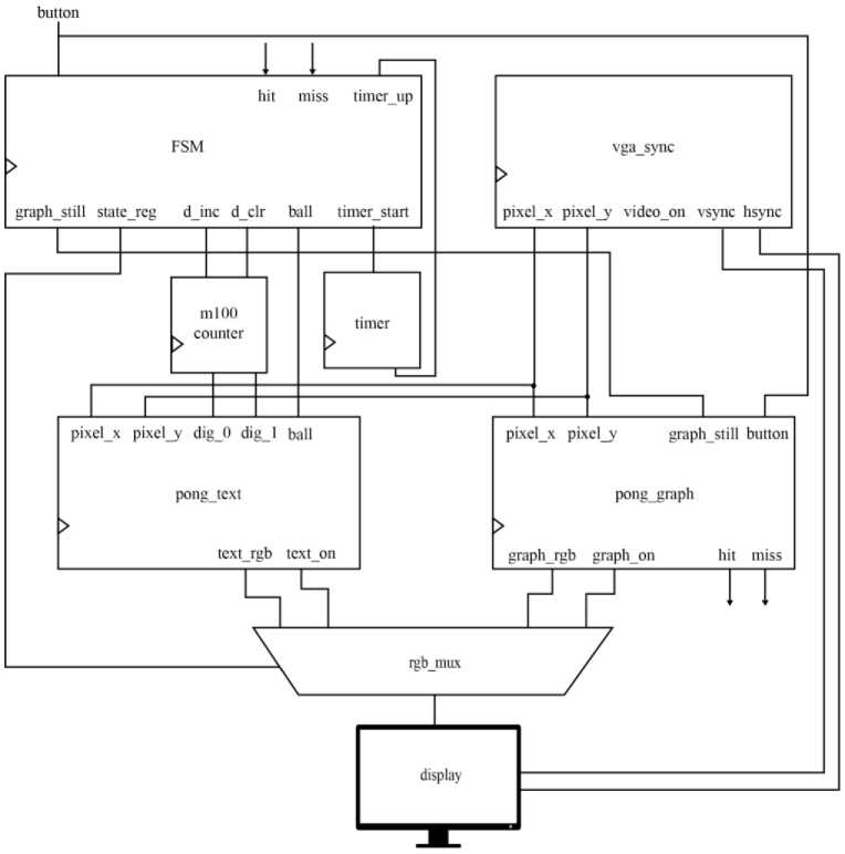
Fig.1. Structure of pong game
In computer monitors, where the capacity to transmit clear, detailed images is crucial, VGA is a high-resolution video standard. The VGA monitor is controlled by five different signals: Horizontal synchronization, Vertical synchronization, red, green, and blue. The three-color signal is collectively called RGB output. This discussion is about VGA display control.
There are many types of VGA screens. This conversation is built around a 640 by 480 VGA screen. The VGA screen's pixel rate is 25 MHz, indicating that 25 million pixels are processed every second. VGA display drive by an input clock signal. So, it is an important factor to fix the clock frequency for the 640 by 480 display. The pixel rate will be the clock frequency of the display. We calculate the pixel rate from equation (1).
p x l X 5 (1)
Here, p = 800 pixels/line (number of horizontal pixels), l = 525 lines/screen (number of vertical lines), and s = 60 screens/second (speed of screen change per pixel). After putting the value in equation (1) we found that a 25 MHz clock needed to produce a 640-by-480 resolution VGA display to produce pixels.
Keep in mind that this resolution is also referred to as VGA mode. The visible area of the monitor is the central rectangle. The upper left corner of the display area serves as the origin and is at (0, 0), bottom right corner of the display is at (639,479). While the x dimension increases from left to right, the y dimension expands from top to bottom. The horizontal and vertical signals are used to control the scan rate of the display. The horizontal signal scans the display pixel row and the vertical scan scans the entire screen.
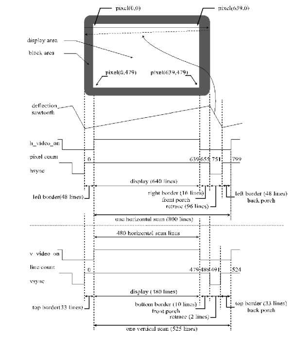
Fig.2. Horizontal and vertical VGA sync
-
3.3. VGA Color Signal
RGB color output controls the intensity and color depth of the VGA display and varies the graphics color according to the controller command. VGA displays are based on additive color display which contains three color signals. These three (Red Green Blue) colors signal is a 24-bit signal. Each signal is an 8-bit signal which will increase the depth of the color with the increasing number of the 8-bit binary signal.
|
Color |
Byte binary (red,green,blue) |
Hexadecimal (red,green,blue) |
|
Red |
255, 0, 0 |
FF, 0, 0 |
|
Green |
0, 255, 0 |
0, FF, 0 |
|
Blue |
0, 0, 255 |
0, 0, FF |
Fig.3. VGA color combinations
In our work, we use Cyclone IV E FPGA board. Which provides the VGA synchronization signals directly, and the
Analog Devices ADV7123 triple 10-bit high-speed video DAC (only the higher 8-bits are used) is used to produce the analog data signals (red, green, and blue). It could support the SXGA standard (1280 × 1024) with a bandwidth of 100MHz [17].
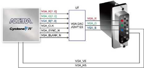
Fig.4. Connections between FPGA and VGA [17]
The monitor's horizontal synchronization (hsync) input receives an active-low pulse of a specific duration, signaling the end of one row of data and the beginning of the next. After the hsync pulse, which is followed by the displayed interval, the data (RGB) output to the monitor must be turned off (driven to 0 V) for a period known as the back porch. The RGB data drives each pixel in turn across the row being displayed during the data display interval. The RGB signals must once more be off during a period known as the front porch before the next hsync pulse can be generated.
-
3.4. Object Generation
Graphic generation is the visual output of the display. What we want to show or not to show completely depends on graphics generation. Graphics is controlled by the change of the pixels. To create the appearance of smooth, fluid motion graphics, pixels must be refreshed faster than the response rate of the human eye. So, the graphics generation circuit must be appropriate for changing the display graphics. The graphics generation circuit generates the 24-bit RGB signal for the VGA port.
data/control video_on pixel_x pixel_y
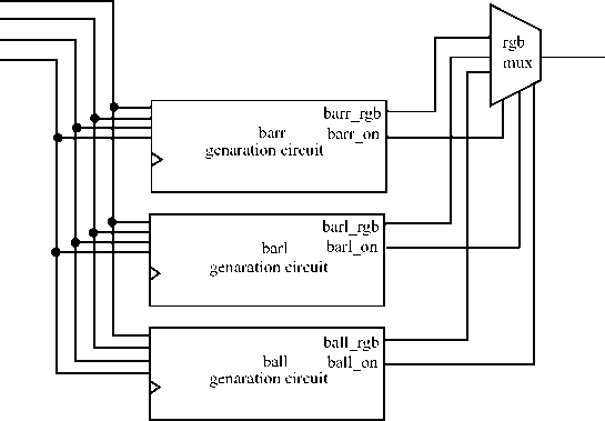
Fig.5. Object generation circuit [1]
For our discussion purposes, the circuit is divided into three categories: bit-mapped scheme, tile-mapped scheme, and object-mapped scheme. In the bit-mapped scheme, the data that will be shown on the screen is stored in video memory when using a bit-mapped method. The pixel of the x-coordinate and pixel of the y-coordinate signals provide the address, and each pixel of the screen is directly mapped to a memory word. A graphics processing circuit that additionally retains relevant information in the video memory continuously updates the screen. 640×480 resolution needs 30700 pixels on the screen and each pixel is 24 bits of color. For the monochrome display bit-mapped scheme needs: 30700×24 =7372800 ≈ 7400K.
Object mapping is used to generate objects for the VGA display. The information will be mapped using the vertical and horizontal axis coordinates. There are data/control signals for the pixel data and control the position of the pixel. There is a video-enable signal to activate the object visualization. The output of the object mapped scheme is RGB signal and object on for the control of the object on timing. The RGB signal from the different objects will be multiplexed by an RGB multiplexer. In the tile-mapped scheme, raster graphics are two-dimensional matrices that store color and are commonly referred to as image tiles. The font of the character set is made up of tiling patterns. There are many different fonts available. We select something like an 8 by 16 font (i.e.,8-columns-by-16-rows). Each character in this font is a pattern of 8 by 16 pixels. The screen is divided into 8-by-8 square pixels as tiles. The 640×480 pixel-oriented screen becomes an 80-by-60 tile-oriented screen. 4800 words are needed for the tile memory. For example, there are 47 patterns. Each word should contain 8 bits and the size of the memory is 38.4K bits. 8-by-8 tile pattern requires 64bit and the 47 patterns need 3K bits. The overall tile memory requirement is 41.4K bits.
Three schemes can be mixed to generate a full screen. However, these three schemes have different memory requirements. Object map scheme is mandatory for this discussion because the game object is created by object map scheme. But tile map and bit map can be replaced by each other. From the above calculation, it is clear that a tile map consumes less memory than a bit map. So, the tile-mapped scheme processes faster than the bit-mapped scheme. It will be best to select a tile-mapped scheme for this game design.
-
3.5. Object Animation
-
3.6. Automatic Paddle Animation
First of all, we try to animate the paddle. There is one paddle and a ball as an object on the game screen. The game starts with the animation of the object. We can see below two object animations and the direction of the animated object:
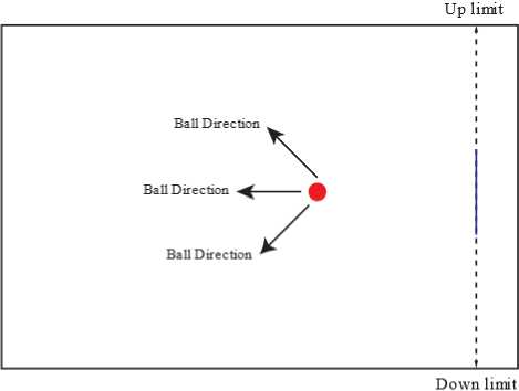
Fig.6. Object animation
In general view, paddle animation is nothing but paddle up and down but it’s not as simple as everyone thinks. In deep analysis, paddle animation is the change of pixel activation and the change of the pixel color according to the command. In this game, the paddle moves up and down, so it moves to the y-coordinate of the screen. There will be two states for the animation. The present state indicates the present location of the paddle and the next state moved the paddle to a new position according to the input signal command. Paddle animation input signal control by push button. There is another signal for still graphics which indicates the still screen of the game. When still graphics signal is available, the paddle center will stand in the 284 number pixel.
Ball animation is another important part of the game. For ball animation, we have to replace four boundary constants with four signals. Then create two registers for x-coordinate and y-coordinate boundaries. The animated ball usually moves at a constant speed but we can add an extra feature to increase the speed after hitting the paddle. It may change direction when hitting the paddle or the bottom or top of the screen. The velocity of the ball decomposes into x and y coordinates. The values of the velocity can be positive or negative on the axis. There is an additional signal introduced to store the instant value of the ball velocity which will drive the ball from the previous state to the next state.
Automatic paddle animation is used for the game as a player. It will act as a human player which introduces the computerized player.
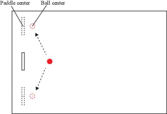
Fig.7. Automatic paddle animation
This animation is controlled by the automatic paddle up-down logic. We have organized it with the calculation of the ball center and automatic paddle center. We use automatic mode switch control by slider switch. When it is available, then the ball will bounce by the automatic bar. We compare these two signals for an automatic paddle up and down.
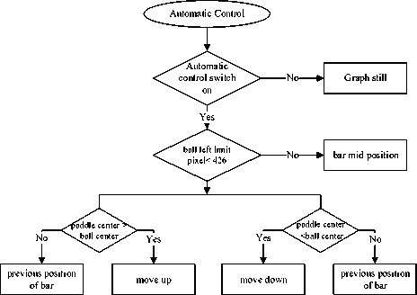
Fig.8. Automatic paddle animation flow
Automatic controlled opponent drives according to the flow chart. It plays like a real opponent and defends the ball to the human paddle. This mode starts with the slider switch command and stops the mode by slider switch of the Altera DE2 board.
-
3.7. Text Generation
Text generation means processing the display pixel in a controlled way. We applying here tile map scheme for character generation. we treated each character as a tile. A tile can be treated as a super tile. For the text display, we use the 7-bit ASCII code for the character tiles. The character of the tile patterns is stored in a ROM and each pattern requires 24*8 bits.
80 tile
Fig.9. Text generation
We use this 8-by-16 character on a 640-by-480 resolution screen, 80 tiles can be fitted for horizontal lines and 30 tiles for vertical lines. The total screen was converted to an 80-by-25 tile screen. We put characters using these scaled coordinates.
Character generation in tile mapped scheme by text generation circuit. We have discussed font ROM and tiles of the screen. Now we have to combine this tile memory and font ROM.
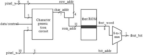
Fig.10. Text generation circuit [1]
First of all, we have to generate coordinate pixels. There are two pixels coordinated x and y. So, we introduce two signals for external data and control signals. In the tile map scheme, we involve two stages. The first stage uses the upper bits of the pixel of the x-coordinate and y-coordinate to generate tile code. The second stage uses this code to generate the pixel’s value. In the first stage pixel_x [9:3] and pixel_y [8:4] signal provides tile location. 5MSBs of pixel_x and 5MSBs are the input value of the character generation circuit and it converts this bit as a character address for the character ROM location.
In the second stage, Four LSBs (pixel_y [3:0]) of pixel_y concentrated the ASCII code which specifies the current location of the pattern. The output of the font ROM corresponds to an 8-bit row in the pattern in the pattern. The three LSBs of the screen’s x-coordinate (pixel_x [2:0]) specify the desired pixel location and an 8-to-1 multiplexer the pixel as output.
-
3.8. Counter
In the gaming system, two important things are game score and game pause time. So, the counter is necessary for counting the score and decreasing the ball after each circle of the ball's lifetime on the screen.
-
A. Score Counter
The counter counts the score of the game. It counts the score for each hit signal asserted by the paddle. It also counts the ball decrease by the missed signal. It counts the score for each hit signal asserted by the paddle. It also counts the ball decrease by the missed signal. several flip-flop types can be utilized to implement counters. A sequential circuit made up of flip-flops and a clock signal is the most popular design. In this game, the mod- 100 counter is used for score count. It counts scores from 00 to 99. The mod-100 counter starts its operation with a clock signal generated by the human control paddle. If the 50hz clock is available then it starts counting or it will wait for the clock signal. If the reset signal is 0 and the clock is available then it increments score digit 1 for each clock signal peck. This score is counted firstly from 0 to 9 then the 1st digit will be 1 and the 2nd digit will circulate from 0 to 9 and then it increments from 2 to 9. This count continues for the duration of the ball count. When the ball count is 0 then the count is over and the counter flipflop will refresh Its data. Then it prepared for the next count and the score remains at 00 and the ball is in 4.
B. Interval Counter
3.9. Game Controller
4. Result and Discussion4.1. Game Implementation Process
The two-second timer is implemented for the interval of the game over and the new game state. The timer module uses the 60-Hz signal to delay and reset the game. It pauses the video signal of the previous state for the interval between the transition of the screen. It starts counting when the timer start signal is asserted and activates with the activation of the timer stop command. It is also a clock signal-based counter which is implemented for the interval between the new game and game over.
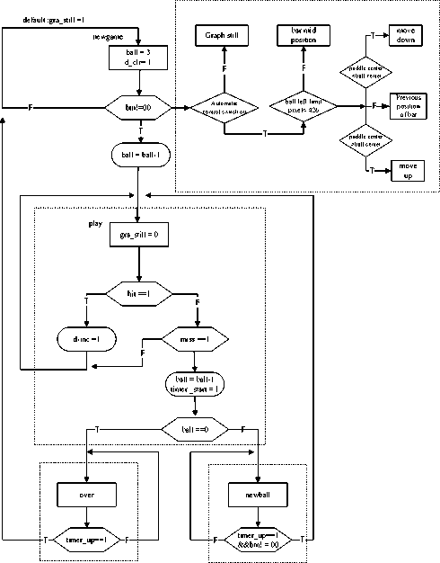
Fig.11. Game control ASMD
Pong's top level consists of a video synchronization circuit, object subsystem, and score counter subsystem. This total game system is based on the ASMD chart. The ASMD is divided into five different states. The FSM moves between new game state, play state, automatic opponent state, new ball state, and game over state.
The FSM is in a new game state which starts with pressing the button and the FSM moves to play state and automatic play state. In the play state, the FSAM checks the hit band miss signals continuously. When the hit signal is activated, the d-inc (score increment signal) is asserted for the score counter count start. But miss signal asserted for activate 2-second timer activation and decrement the ball. Then the FSM checks the remaining ball. If the ball count is 0 then the FSM moves to game over state but if the ball is greater than 0 then the FSM moves to the new ball state. The FSM waits in the new ball state until a 2-second interval is up and the button is pressed. The FSM is in overstate until the timer count of 2 seconds is up. When the timer count is up then it moves to the new game state for the new game. The automatic opponent state starts with the automatic switch activation. Automatic control FSM starts with the movement of the ball. It defends the ball and moves according to the ball's center movement. If the ball center moves up then the automatic paddle moves up to follow the ball center and moves down with the ball center position. The game text is also controlled by FSM. The welcome text, new game start text, and rules of the game are displayed when the FSM is in the new game state. Game over text is also shown with the moves of the FSM.
In this chapter, we will discuss the result of our work as well as the visual output. In our work we use ModelSim logic simulator and Quartus Prime lite for compilation We have implemented a VGA synchronization circuit on ModelSim and simulated it. We also provide experimental results of VGA synchronization. Quartus Prime tools are used for the calculation of resource utilization and power consumption analysis. We show different modes of the game, resource utilization by pixel generation circuit, and power consumption, and also provide a comparison between different modes of the game.
Our Verilog HDL code is simulated using ModelSim. After a successful simulation, we use Quartus Prime to synthesize and analyze our design. When the synthesis is finished, we upload our design to the Altera DE2 board, connect a monitor to the board's VGA connector, and then execute our design.
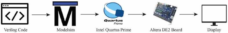
Fig.12. Game implementation process
-
4.2. Modelsim Simulation Result
After the logic simulation, we get a waveform for the VGA synchronization. Timing format 640×480@60Hz scans at 60 frames per second. The video_on signal exists till 639 horizontal counts. Horizontal synchronization is available when the horizontal count is 656 and vertical synchronization is available when the vertical count is 513. VGA synchronization simulation results are given below:
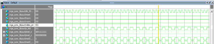
Fig.13. video_on turns off at 639 horizontal scans
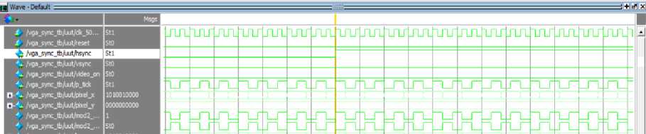
Fig.14. The hsync signal is on
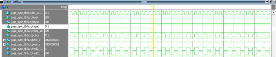
Fig.15. The vsync signal is on
-
4.3. Resource Utilization
-
A. Resource Utilization by Pixel Generation Circuit
The pixel generation circuit has three major parts. They are bit-mapped scheme, tile-mapped scheme, and objectmapped scheme.
Table 1. Resource Utilization by Pixel Generation
|
Resources |
Utilization |
||
|
Bit-map |
Tile-map |
Object map |
|
|
Total logic elements |
131 |
42 |
241 |
|
Combinational LUTs |
123 |
42 |
219 |
|
Total Registers |
71 |
23 |
79 |
|
Maximum fan out |
80 |
349 |
80 |
|
Total memory bits |
256 |
0 |
0 |
In the analysis, the bit map utilizes 0.11% of the elements whereas the tile map utilizes 0.036% of the elements. In the general view, it seems very small but it is not negligible when we use it for multiplayer game.
-
B. Comparison Between Different Modes
To finish these three different modes of the game, we analyze these three modes of game utilization and power consumption reports.
Table 2.Resource utilization of different modes of game
|
Resources |
Utilization |
||
|
Single-player |
Two players |
Human vs Automatic |
|
|
Total logic elements |
1491 |
1521 |
1667 |
|
Combinational LUTs |
1446 |
1508 |
1563 |
|
Total Registers |
115 |
116 |
121 |
|
Maximum fan out |
347 |
347 |
350 |
In the single-player mode, the design required 1.3% of the total logic elements whereas the two-player mode and Automatic player mode use 1.32% and 1.456% of total logic elements. Which is looking very small but in the giant scale integration, it is significant and it provides a delay to the operation.
Table 3. Power consumption of different modes of game
|
Resources |
Power Consumption (mW) |
||
|
Single-player |
Two players |
Human vs Automatic |
|
|
Core static thermal power |
98.60 |
98.60 |
98.61 |
|
Core dynamic power |
0 |
0 |
0 |
|
I/O thermal power |
45.76 |
45.73 |
46.13 |
|
Total thermal power |
144.37 |
144.33 |
144.74 |
The power consumption of different modes is so close to each other because there is a little bit of change in logic elements. So, the elements consume the same kinds of power. But we can see that the fan out of the Automatic and human mood is greater than the other two operations, so the input-output thermal power consumption is high.
4.4. Complete Game
5. Conclusions
This is the complete game screen. There are two bars animated up and down in direction and the ball is animated in different directions. The text is displayed successfully and the text of the score is updated according to the counter.
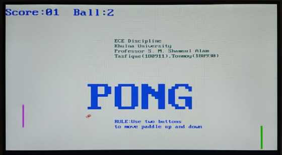
Fig.16. Complete game screen
This paper provides a basic overview of FPGA-based game implementation. There are different types of gaming modes discussed here and compared according to different parameters. The utilization of logical elements, memory requirements, and power consumption are discussed using Quartus Prime tools. We find the best methods and follow the fastest processing and low power consumption scheme for design. We have tested the accuracy of the game-playing mode and shown it in the result section with real-time images. Graphics generation and pixel mapping are calculated with the requirement and well-furnished way. The automatic player played and moved like a real player with the ball position. We have reduced external controllers and processors which make flexible and fastest processing. We check all the requirements of memories and power dissipation for every scheme and choose the best methods for designing. We have used minimum logical elements (<1%) of the Altera DE2 board for the design. This is just a basement of this path of research which can be extended in the future.
In the future, it can add an audio system and play the game easily with the help of a keyboard and mouse. The game will be more interesting when we add more game levels and multi-layered features to it. We can also be able to save game scores using memory.
References Design and Implementation of Multi Player Pong Game using Altera DE2 Board
- P. P. Chu, “FPGA prototyping by Verilog examples: Xilinx Spartan-3 version.” John Wiley & Sons, 2011.
- I. Nagarjuna and P. Ramesh, "An FSM Based VGA Controller with 640⨯ 480 Resolution," International Journal of Engineering and Advanced Technology (IJEAT), vol. 2, no. 4, pp. 881-885, 2013
- F. Ying and X. Feng, "Design and implementation of VGA controller using FPGA," International Journal of Advancements in Computing Technology, vol. 4, no. 17, 2012.
- S. Sivasathya and K. Kannadasan, "Design of VGA monitor controller in FPGA using on-chip embedded array RAM," Int. J. Technol. Eng. Syst, vol. 6, no. 1, pp. 27-31, 2004.
- P. Pokharel, B. Bhatta, and A. D. Darji, "Optimized drivers for PS/2 and VGA using HDL," in 2011 IEEE International Conference on Computer Science and Automation Engineering, 2011, vol. 3: IEEE, pp. 262-266.
- R. A. Wasu, V. R. Wadhankar, “Design and Implementation of VGA Controller on FPGA” International Journal of Innovative Research in Computer and Communication Engineering, Vol. 3, pp 7224– 7231, 2015.
- W. Hong-bin, Z. Zhe, C. Xu-hui and W. Yuan-bin, "VGA Display Driver design Based on FPGA," 2019 IEEE/ACIS 18th International Conference on Computer and Information Science (ICIS), Beijing, China, 2019, pp. 530-535, doi: 10.1109/ICIS46139.2019.8940166.
- B. M. Krishna, V. S. Swaroop, K. G. Deepika, and H. Khan, "PS2-VGA peripheral based character display using FPGA," International Journal of Computer Applications, vol. 48, no. 9, pp. 1-5, 2012.
- G. Wang, Y. Guan, and Y. Zhang, "Designing of VGA character string display module based on FPGA," in 2009 International Symposium on Intelligent Ubiquitous Computing and Education, 2009: IEEE, pp. 499-502.
- V. D. Nguyen, Duck Hunt FPGA game, a project on UML and digital design. California State University, Long Beach, 2016.
- K. Liu, Y. Yang, and Y. Zhu, "Tetris game design based on the FPGA," in 2012 2nd International Conference on Consumer Electronics, Communications and Networks (CECNet), 2012: IEEE, pp. 2925-2928.
- A. Mishra, A. Kumar, and R. Parihar, "Design and FPGA Implementation of Space Shoot Game," International Journal of Control Theory and Applications, vol. 10, no. 30, 2017.
- A. Jarusauskas, "FPGA based VGA driver and arcade game," University of Sussex, vol. 2010, 2009.
- R. Szabó and A. Gontean, "Pong game on FPGA with CRT or LCD display and push button controls," in 2014 Federated Conference on Computer Science and Information Systems, 2014: IEEE, pp. 729-734.
- Li, Z., Jiang, Y., Guo, Y. (2019). An Independent VGA Controller Based on SOPC with Three Pixel-Mapped Schemes. In: Xu, W., Xiao, L., Li, J., Zhu, Z. (eds) Computer Engineering and Technology. NCCET 2018. Communications in Computer and Information Science, vol 994. Springer, Singapore. https://doi.org/10.1007/978-981-13-5919-4_2
- Mishra, A., Kumar, A., Parihar, R. (2018). VGA Application in Text Display Using FPGA. In: Singh, R., Choudhury, S., Gehlot, A. (eds) Intelligent Communication, Control and Devices. Advances in Intelligent Systems and Computing, vol 624. Springer, Singapore. https://doi.org/10.1007/978-981-10-5903-2_163
- Altera DE2-115 User Manual, available on https://www.intel.com. [Accessed: 22-Jan-2023].
