Design and Implementation of Three Phase Unbalanced Voltage Motor Controller

Author: M. A. A. Mashud, S. C. Barman, M. R. A. Bhuiyan, Md. Serajul Islam
Journal: International Journal of Intelligent Systems and Applications(IJISA) @ijisa
Article in issue: 10 vol.5, 2013.
Free access
A state-of-the-art-technology was used to design the unbalanced three phase motor controller. The fluctuation of line voltage has been questioned in recent times due to the use of heavy powered machine with three phases. This paper is focused on deriving a control scheme to drive a three phase motor that could be used in industry or households. The very simple circuitry has been employed in this design. To do this, extensive MATLAB analysis and PSpice software was conducted in order to optimize the control system and finally the results are practically verified.
Industry, Line Voltage, Three Phase, Unbalance, Spark And Damage
Short address: https://sciup.org/15010476
IDR: 15010476
Text of the scientific article Design and Implementation of Three Phase Unbalanced Voltage Motor Controller
Published Online September 2013 in MECS
Fluctuations of line voltages are of special attention now-a-days. A need for reasonable power is required to smoothly operate electrical and electronic appliances. Quite often it happens that line voltages of some phases go down to a low level or high level. Therefore the line voltage becomes unbalanced. A large number of machines used in industries such as garments sectors, agricultural industry, cement factory, ceramic or glass factory, cold storage, dying sectors and so on are needed balanced voltage. For these erratic conditions of line voltages the valuable machines becomes damaged. Besides sometimes it makes sparking and makes serious problems in industry such as burning.
Under such erratic conditions of line voltage, in our country re-wireable fuse or miniature circuit breaker are normally used to protect different households from under and over-voltage conditions is explained in S. Islam et.al, [1]. Considering this factor, a protective device like over-voltage and over-current with time delay unit has been developed for ensuring a dependable and an effective protection to small households in year 1992 that explained in S. Islam et.al, [2]. This system is relatively slow and designed in transistor based. For the better performance another device has been developed to protect households in year 1994 which explained in S. Islam et.al, [3]. The operation speed of this device is better but it was designed in transistor based. In year 2011, another attractive device has been developed for single-phase line to protect electronic appliances from over-load which explained the author M.A.A. Mashud et.al, [4]. In this design transistor module has been replaced by IC module and use Hall Effect principle.
In year 2012, the author M.A.A. Mashud et. al, [5] explained single phase line voltage controller using microcontroller. In this design all electronic components and ICs has been replaced by using a microcontroller. But all the above designs are for single phase line voltage controller.
Now, the author developed a three phase unbalanced line voltage controller. Easily available components and simple circuitry, the system should be beneficial in providing low-cost.
-
II. Design Considerations
The system is divided into six main parts: low-voltage power supply, phase detector circuit, summing circuit, reference voltage source, window detector circuit and relay driver unit. The block diagram and the complete circuit diagram of the developed system are depicted in Fig. 1 and Fig. 2 respectively.
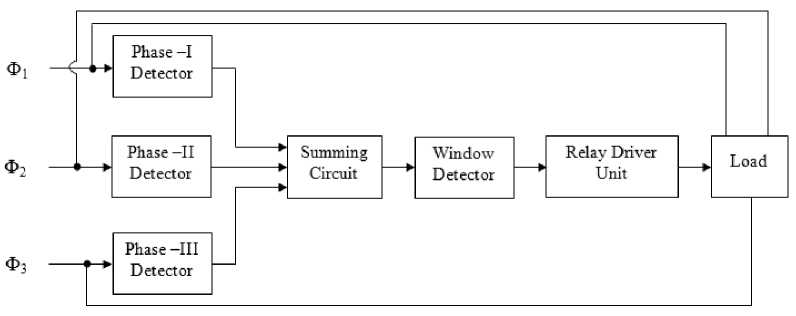
Fig. 1: Block diagram of the developed system
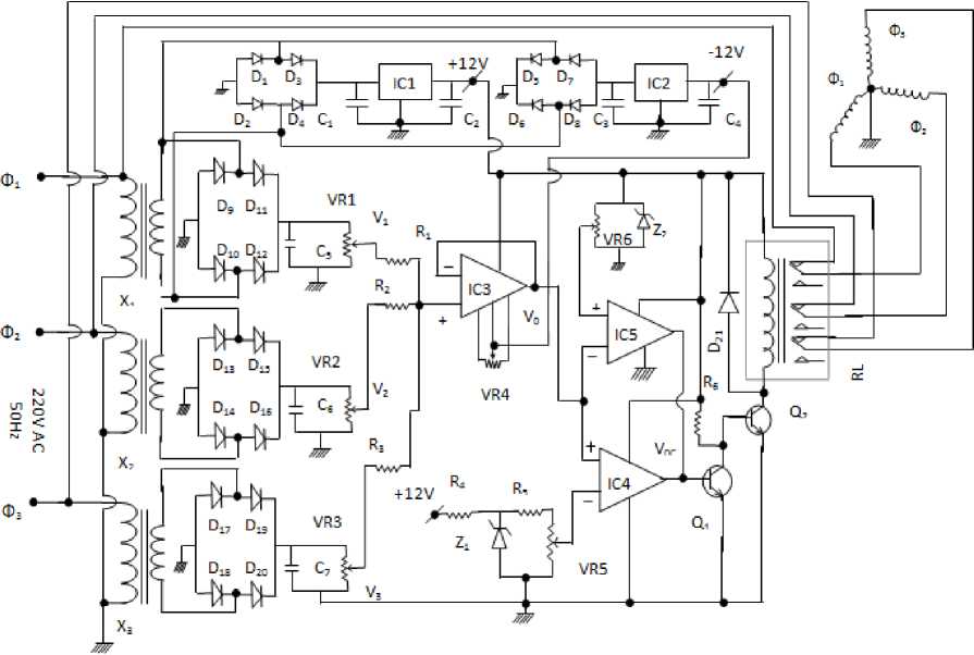
Fig. 2: Complete circuit diagram of the developed system
-
2.1 Low Voltage Power Supply
-
2.2 Phase Detector
Two types of low-voltage power supply are used in this design namely: positive and negative power supply. The positive low-voltage power supply circuit consists of transformer X1, D1, D2, D3, D4, C1, C2, and IC1 [6]. The output of the IC1 is +12V DC. The capacitor C2 is connected across the output of IC1 to eliminate the high frequency noise. The negative low-voltage power supply circuit consists of transformer X1, D5, D6, D7, D8, C3, C4, and IC2. The output of the IC2 is -12V DC. The capacitor C4 is connected across the output of IC2 to eliminate the high frequency noise.
Phase-I Detector
The phase-I detector circuit consists of transformer X1, D9, D10, D11, D12, C5 and VR1. The bridge rectifier circuit produces a pulsating DC voltage. Eliminating the pulsating DC produces pure DC by using capacitor filter [7]. The filter capacitor C5 is connected across the output of the rectifier circuit. A potentiometer VR1 is used for setting the output voltage to a desired value. In this design we have used this value to +2V DC denoted by V1.
Phase-II Detector
The phase-II detector circuit consists of transformer X2, D13, D14, D15, D16, C6 and VR2. The bridge rectifier circuit produces a pulsating DC voltage. Eliminating the pulsating DC produces pure DC by using capacitor filter. The filter capacitor C6 is connected across the output of the rectifier circuit. A potentiometer VR2 is used for setting the output voltage to a desired value. In this design we have used this value to +2V DC denoted by V 2 .
Phase-III Detector
The phase-III detector circuit consists of transformer X3, D17, D18, D19, D20, C7 and VR3. The bridge rectifier circuit produces a pulsating DC voltage. Eliminating the pulsating DC produces pure DC by using capacitor filter. The filter capacitor C7 is connected across the output of the rectifier circuit. A potentiometer VR3 is used for setting the output voltage to a desired value. In this design we have used this value to +2V DC denoted by V 3 .
-
2.3 Summing Circuit
-
2.4 Reference Voltage Source
-
2.5 Window Detector
-
2.6 Inverter
The summing circuit consists of R 1 , R 2 , R 3 , IC3 and VR4 [8]. In this design VR4 is used to minimize the output offset. The non-inverting configuration is employed in this work. The output voltage V0 is equal to the sum of the input voltages applied to the noninverting. The output voltage equation is expressed in equation (1) as follows:
V 0 = V 1 + V 2 + V 3 (1)
Two types of voltage reference sources are used in this design i.e. lower limit level reference and upper limit level reference. The lower limit level reference source consists of Z1, R4, R5 and VR5 [9]. The upper limit level reference source consists of Z2 and VR6.
When it is needed to determine an unknown input between two precise reference thresholds Vut and Vlt then window detector is used. The window detector circuit consists of IC4 and IC5 [10]. In this case the output summing circuit V0 voltage is applied to the (-) input of IC5 and to the (+) input of IC4. An upper limit level reference voltage Vut is applied to the (+) input of IC5, whereas the lower limit level reference voltage Vlt is applied to the (-) input of IC4. The outputs of IC4 and IC5 are connected to form a single output V0C. When V0 is between Vut and Vlt the output V0C is high. However, when V0 goes above Vut or drops below Vlt, the output V0C switches low or to 0 V.
The inverter is used to complement or invert a signal. It has a single input and a single output. The symbol and truth table for the inverter gate are shown in Fig. 3(a) and (b), respectively.
Input A
Output X
(a) Symbol
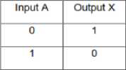
(b) Truth table
Fig. 3: (a) Symbol and (b) Truth table of an inverter
In the equivalent transistor circuit of Fig. 4 when a voltage is applied from the output of comparator to A, the transistor will be turned ON, drawing maximum collector current. Hence, whole of Vcc will drop across R thereby sending B to 0V. With 0V applied at A, the transistor will be cut OFF and the output B, therefore, will go to Vcc. Obviously, in each case, output is the opposite of input [11].
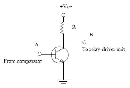
Fig. 4: Inverter circuit
-
2.7 G. Relay Driver Unit
Transistor as a Switch
The transistor switch consists of Q1, Q2 and R6. In an electronic circuit, the input signal (1 or 0) is usually applied to the base of the transistor, which causes the collector-emitter junction to become a short or an open circuit. When a transistor is used as a switch it must be either OFF or fully ON. In the fully ON state, the voltage V across the transistor is almost zero and the transistor is said to be saturated because it cannot pass any more collector current ICE. The output device switched by the transistor is usually called the ‘load’.
Calculation of Base Resistance, RB (R6):
The load resistance, which is the collector resistance, is the resistance of the relay coil as shown in Fig. 5.
The 12 V relay used has the coil resistance of 100 Ω. Therefore, R = 240 Ω. The NPN transistor used is 2N3904. Thus, from the datasheet of 2N3904:
Ic(max) = 200 mA, hFE(max) = 300(2)
Taking hFE to be 100 implies that hFE = 100, Rc = 240Ω, Vcc = +12V(3)
But when the transistor is saturated
VCE(sat) = 0.2V, VBE(sat) = 0.7V(4)
Thus at saturation [12]
Ic(sat) = (VCC-VCE) / RC= (12-0.2)/240 = 0.049(5)
Thus A = 49mA the base resistance, R was chosen to be 4.7 kΩ to ensure saturation which will give base current of
(12 - 0.7)V / 4.7 KΩ = 2.48 mA > I c /h FE (i,e 0.49mA)
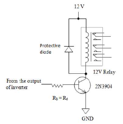
Fig. 5: Circuit diagram of the relay driver unit
Relay as a Switch
A relay provides total isolation between the triggering source applied to the terminal and the output. This total isolation is important in many digital or analog applications and it is a feature that certain semiconductor switches (e.g. transistors, diodes and integrated circuits) cannot provide. Also, the contacts are normally rated for currents much higher than the current rating of semiconductor switches [13].
The minimum value of base current is then obtained
I B(min) = I C(sat) / h FE = 49mA / 100 = 0.49mA (6)
Therefore, the voltage across the base resistance R B is
V B = V in – B BE(sat) (7)
Protective Diode
If the load is a motor, relay, or solenoid (or any other device with a coil), a diode must be connected across the load to protect the transistor from the brief high voltage produced when the load is switched OFF. In our design a protection diode D21 is connected ‘backwards’ across the load, in this case a relay coil. The diagram in Fig. 6 shows how a protection diode is connected ‘backwards’ across the load, in this case a relay coil [14].
When Vin is the output voltage of the inverter which is approximately equal to Vcc (+12V)
As a result, VB = 12 – 0.7 = 11.3V, then the maximum value of RB is
R B(max) = V B / I B = 11.3 / 0.49 = 23.06 KΩ (8)
The maximum value of RB that will allow a minimum I B of 0.48 mA to flow was calculated by Ohm’s Law. The actual value used should be much less. Therefore,
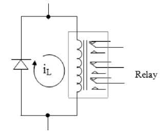
Fig. 6: Illustration of a protection diode
The circuit of our design uses a relay to isolate an electric motor from the logic devices. Notice that the logic circuit and motor have separate power supplies. When the output of the inverter goes HIGH, the transistor is turned on and the NO contacts of the relay snap are closed. The motor operates by providing a rotary motion, which drives the mechanical devices that result in machine ON. When the output of the inverter goes LOW, the transistor stops conducting and the relay contacts spring back to their NC position. This turns off the motor, thereby stopping the machine.
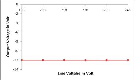
Fig. 9: Negative low-voltage power supply
-
III. Results and Discusion
The transfer function of three phase line voltage is implemented in Simulink (Matlab). The result is given in Fig. 7. This figure shows the line to neutral voltages and line to line voltage. Hence it seen that the line voltages is in normal condition.
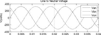
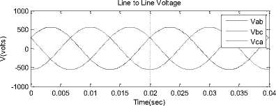
Fig. 7: Simulation in Simulink
The reference voltage source was design in very confidently. In this design we had varied the input ac voltage from 198 volt to 248 volt and the output was observed and recorded. The lower-limit reference unit produces exactly 5.999 volt DC and the upper-limit reference unit produces exactly 6.001 volt DC. The practical output waveform of lower limit and upper limit reference voltage source is shown in Fig. 10 and Fig. 11 respectively.
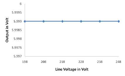
Fig. 10: Lower-limit level refernce voltage
The complete hardware design is implemented and very satisfactory results are obtained. Firstly, the low voltage power supply unit was designed for highly regulated output to bias the major components of this system. In this design we had varied the input ac voltage from 198 volt to 248 volt but the output was remain constant at +12 volt and -12 volt DC. The experimented output waveforms of this unit are depicted in Fig. 8 and Fig. 9 respectively.
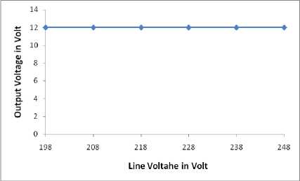
Fig. 8: Positive low-voltage power supply
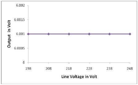
Fig. 11: Upper-limit level reference voltage
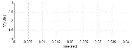
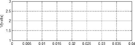
The output of the phase detectors circuit is shown in Fig. 12. From figure it is clear that phase-I, phase-II and phase-III produces exactly 2 volt DC when the line voltages are at normal condition that means no fluctuations in the line voltages. The output of the detector ciotcuit is measured by voltmeater and also osciloscope and obtained the result is very nearly to 2 volt DC.
3-----------------------1-----------------------1-----------------------1-----------------------1-----------------------1-----------------------1-----------------------1-----------------------
-
2.5--------- j.--------i--------i--------^--------j.--------i--------i--------
- j 2—--h
-
1.5---------!■------------------------i---------!■------------------------
-
10 0 005 0.01 0.015 0.02 0.025 0.03 0.035 0.04
Time (sec)
(a) Phase – I detector
(b) Phase – II detector
Time (sec)
(c) Phase – III detector
Fig. 12: Output of phase detectors at normal line voltages (simulation)
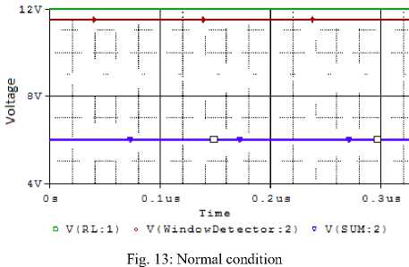
The output of the detectors circuit is applied to the adder circuit. The adder circuit provides the output exactly equal to the sum of the input voltages. In this design, when no fluctuation occurs on the line voltages the adder circuit produce exactly 6 volt DC. In this case the output of the window detector is high (near to 11.5 volt). The transistor switched ON, hence the relay activated and the device is ON. The graphical representation of this condition is shown in Fig. 13. When the line voltages fluctuates, this may goes to up or down than the normal condition.
If the voltage of any one or more phase goes to down, the output of adder circuit becomes less than 6 volt (V0 < 6 volt). The output of window detector is low (near to 0 volt). The transistor switched OFF, hence the relay turns OFF. Therefore the device becomes OFF. The graphical representation of this condition is shown in Fig. 14.
Fig. 14: Phase voltage goes down
If the voltage of any one or more phase goes to up, the output of adder circuit becomes greater than 6 volt (V 0 > 6 volt). Also the output of window detector is low (near to 0 volt). The transistor switched OFF, hence the relay turns OFF. Therefore the device becomes OFF. The graphical representation of this condition is shown in Fig. 15.
IV. Conclusion
The system was successfully developed and was put under a series of tests for ascertaining its performance as a protective device. Its performance was strong and very satisfactory results were obtained. When any one of the three phases fluctuates, the motor was turned off. The safety of the equipment protection by the device under any undesired transient condition of the main supply was ensured. This device had a very high sensitivity. It was also simple in design, reliable in operation and cost competitive with any other product available in the market. From the above analysis, it is
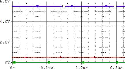
Time о V(RL:1) о V(WindowDetector:2) vV(SUM:2)
Fig. 15: Phase voltage goes up concluded that this device can easily protect three phase motor against fluctuation of line voltages and over load current.
References Design and Implementation of Three Phase Unbalanced Voltage Motor Controller
- M. S. Islam and M. A. Zulquarnain, (1991), Journal of the Bangladesh Electronics Society, pp 31.
- M. S. Islam and M. Kamruzzaman, (1992), Journal of the Bangladesh Electronics Society, Vol.2,No. 1, pp 29.
- S. Islam, (1994) Nuclear Science and Applications, Vol. 3, No. 2.
- M.A.A. Mashud, E. Haque and S. Islam, (2011), Jahangirnagar Physics Studies, Vol. 17, pp151 ISSN 1999-6632.
- M.A.A. Mashud, M.A.A. Tariq, M. Shamim Hossain and Md. Serajul Islam, (2012), I. J. Information Sciences and Techniques (IJIST) Vol.2, No.4, pp 49-56
- V. K. Mehta and R. Mehta, (2007) Principles of Electronics, S. Chand & Company Ltd. New Delhi, pp 438.
- Allen Mottershead, (1998), Electronic Devices and Circuits, Prentice-Hall of India Pvt. Ltd. New Delhi-110001, pp 35.
- R.A. Gaykwad, (2000), Op-Amps and Linear Integrated Circuits, Prentice-Hall of India Pvt. Ltd. pp 206.
- R.P. Malvino, Electronic Principles, Tata McGraw-Hill Publisher Company Ltd. New Delhi, Sixth Edition, pp 144
- R.F. Coughling and F.F. Driscoll, (1992), Operational Amplifiers and Linear Integrated Circuits, Prentice-Hall of India Pvt. Ltd. New Delhi-110001, Fourth Edition. pp 65.
- R. P. Jain, (1998), Modern Digital Electronics, Tata McGraw-Hill Publishing Company Ltd, New Delhi 110008, Second Edition, pp 97.
- Bell, Electronic Devices and Circuits, Prentice-Hall of India Pvt. Ltd. pp 83.
- B.L. Theraja and A.K Theraja, (2002) A Textbook of Electrical Technology, S. Chand & Company Ltd. New Delhi, pp 2105.
- R.L Boylestad and L. Nasheslky, (2007), Electronic Devices and Circuit Theory, Prentice-Hall of India Pvt. Ltd. pp 803.
