Design and Simulation of Biomimetic Controller

Author: Chaitra H., Punith Kumar M.B.
Journal: International Journal of Engineering and Manufacturing @ijem
Article in issue: 5 vol.15, 2025.
Free access
The development of upper limb prostheses poses a significant challenge in providing amputees with sensory feedback. This paper presents a novel approach by proposing a biomimetic circuit specifically designed to replicate the behavior of slowly adapting (SA-I) afferents, which are responsible for encoding sustained indentation and offering crucial sensory feedback. The circuit has been meticulously designed and simulated using Cadence Virtuoso software, a powerful tool for circuit design and optimization. To validate the functionality and performance of the biomimetic circuit, a grid of mechanoreceptors is simulated and tested, providing realistic inputs for the circuit. The circuit successfully emulates the response of SA-I afferents to sustained indentation, exhibiting a slowly adapting discharge that linearly correlates with the depth of indentation. This ability to replicate the natural behavior of SA-I afferents represents a significant advancement in the field of providing sensory feedback for upper limb prostheses. The biomimetic circuit holds great promise in addressing the crucial need for sensory feedback in upper limb prosthetics. By integrating this circuit into upper limb prostheses, amputees can experience more intuitive and realistic sensations during interactions with their environment. The replication of SA-I afferent behavior provides users with vital information about the magnitude and duration of applied forces, enhancing their overall perception and control of the prosthesis. The findings of this study contribute to the ongoing progress in the field of prosthetics, particularly in the development of more sophisticated and advanced upper limb prostheses. The successful implementation and simulation of the biomimetic circuit demonstrate its potential as a viable solution for providing amputees with enhanced sensory feedback, ultimately improving their quality of life and reintegrating them into daily activities more seamlessly. The new approach emphasizes the development of a biomimetic circuit tailored to replicate SA-I afferent behavior. The proposal addresses the challenge of providing sensory feedback in upper limb prostheses. The study utilizes Cadence Virtuoso software for precise design, layout, and simulation, offering a practical solution for realistic sensory feedback. By accurately emulating the response of SA-I afferents to sustained indentation, the circuit holds the potential to significantly enhance amputees' quality of life and integration into daily activities. The proposed circuit contributes to the advancement of upper limb prosthetics and represents a significant leap forward in achieving more intuitive and authentic sensory experiences for prosthesis users.
SA-I Afferents, Indentation, Cadence Virtuoso
Short address: https://sciup.org/15019953
IDR: 15019953 | DOI: 10.5815/ijem.2025.05.01
Text of the scientific article Design and Simulation of Biomimetic Controller
The fields of neuroscience and robotics are converging as machines. Sensing and interacting with objects are the main goals of prosthetic hands. In humans, low-threshold cutaneous mechanoreceptors (LTMRs) perform tactile information encoding “Ref. [1]”. They respond to mechanical stimuli and generate spikes. Cutaneous afferents are categorized into several types, namely Merkel cells, Meissner corpuscles, Ruffini endings, and Pacinian corpuscles. There are four classes determined by two characteristics of neural firing. In the case of the first characteristic, slowly adapting (SA) afferents generate spikes in response to static stationary external force or pressure “Ref. [2]”. The second characteristic is based on the size of the receptive field and includes type-I afferents that are near to skin surface. SA-I fibers consist of approximately 25% tactile fibers and exhibit multiple branches in proximity to the skin's surface “Ref. [3]”. This branching creates Relative fields (RFs) for each SA-I afferent that have an area of 10sqmm on average.
One particular type of SA afferent, known as SA-I fibers, constitutes around 25% of all tactile fibers. These fibers branch out near the skin surface, forming multiple branches that innervate Merkel discs distributed across various fingerprint ridges “Ref. [4]”. The branching pattern creates receptive fields (RFs) for each SA-I afferent, with an average area of approximately 10 mm2. These RFs allow for the detection and encoding of tactile stimuli across the skin's surface. The development of electronic skins (e-skins) for applications in robotics and prosthetics has sought to replicate the biological characteristics of tactile afferents using neuromorphic chips “Ref. [5]”. By incorporating advanced skin dynamics and neuromorphic design principles, e-skins can offer more sophisticated sensory feedback. Spiking neural networks and neuromorphic techniques have gained prominence in recent years, enabling more accurate modeling and emulation of tactile sensory systems.
Previous approaches utilizing field-programmable gate arrays (FPGAs) involved collecting data from tactile sensors and converting it into spiking activity within the FPGA. However, due to their large size and power consumption, these digital neuromorphic systems are not practical for prosthetic hand applications “Ref. [6]”. Consequently, there is a need to develop neuromorphic complementary metal-oxide-semiconductor (CMOS) circuits that can accurately mimic biological mechanisms and model populations of tactile afferents “Ref. [7]”.Such an approach would be valuable for the creation of future e-skins, particularly in robotic and prosthetic applications where the touch and palpation of objects, shapes, and textures are crucial.
The study of cutaneous low-threshold mechanoreceptors and their role in transmitting tactile information has driven advancements in the development of electronic skins “Ref. [8]”. By incorporating neuromorphic CMOS circuits that mimic the behavior of tactile afferents, e-skins can provide more realistic and advanced sensory feedback. These technological advancements have significant implications for various fields, including robotics and prosthetics, enabling improved touch perception and manipulation of objects, shapes, and textures. In this study, an analog CMOS circuit that utilizes a biomimetic circuit to create complex Relative fields (RFs) “Ref. [9]”.This biomimetic circuit has a small area and low power consumption. It is designed in cadence virtuoso software and it models the spiking activity of SA-I. In biology, skin mechanoreceptors are connected to tactile afferents “Ref. [10]”. This arrangement helps to extract the characteristics of touched objects. The proposed CMOS circuit incorporates the concept of Relative fields (RFs) through the connection of several mechanoreceptors.
The rationality and feasibility of implementing circuit simulation in biomimetic circuit development for e-skin technologies are evident from the advantages it offers. From cost savings and risk reduction to behavior validation and performance optimization, simulation serves as a powerful tool that accelerates the development of accurate and sophisticated electronic skin technologies. By leveraging the capabilities of Cadence Virtuoso software, engineers can confidently design, validate, and optimize biomimetic circuits, contributing to the advancement of sensory feedback in prosthetic hand applications.
2. Literature Review 2.1 Flexible and Stretchable Electronic Skins
Researchers have made significant progress in developing flexible and stretchable eskin materials that can conform to the contours of the human body “Ref. [8]”. Usually, these materials are composed of slender and flexible substrates that are combined with sensors and electronic components. The use of novel materials, such as graphene, carbon nanotubes, and polymers, has allowed for the creation of e-skins that are robust, lightweight, and capable of detecting a wide range of tactile stimuli.
2.2 Bio-Inspired Tactile Sensing
2.3 Neuromorphic Engineering
2.4 Prosthetic Hand Technologies
3. SA-I Afferents
Researchers have drawn inspiration from the human somatosensory system and the properties of Cutaneous mechanoreceptors to design bio-inspired tactile sensing systems. By emulating the behavior and characteristics of mechanoreceptors, such as their response dynamics, spatial resolution, and selectivity to strain energy density, these systems aim to provide more realistic and precise tactile feedback. This approach involves the development of Biomimetic circuits and signal-processing algorithms that replicate the neural encoding and processing mechanisms of the human tactile system.
The field of Neuromorphic engineering has played a significant role in the development of Biomimetic circuits for e-skins. Neuromorphic engineering focuses on designing electronic circuits and systems that emulate the functionality and behavior of biological nervous systems. This approach has led to the creation of spiking neural networks, Neuromorphic chips, and CMOS-based circuits capable of mimicking the neural activity of tactile afferents. These circuits enable the conversion of physical stimuli into spiking neural activity, facilitating the transmission of sensory information in a format similar to that of the human nervous system.
The development of Biomimetic circuits for sensory feedback is closely linked to advancements in prosthetic hand technologies. Researchers and engineers have made significant progress in designing more advanced and dexterous prosthetic hand systems. These systems incorporate e-skin technology and Biomimetic circuits to provide sensory feedback, enabling users to perceive touch, pressure, and texture. The integration of Biomimetic circuits into prosthetic hands has shown promising results in improving the functionality and usability of these devices.
SA-I afferents are densely distributed within the skin, with an estimated density of approximately 100 per square centimeter at the fingertip in both humans and monkeys. Under sustained indentation, these afferents demonstrate a continuous, slowly adapting discharge that correlates directly with the depth of the indentation “Ref. [11]”. SA1 afferents exhibit two notable response characteristics. Firstly, they exhibit heightened sensitivity to points, edges, and curvature, attributed to their selective response to strain energy density or a closely related strain component, like the square of the maximum local compressive strain, regardless of its orientation “Ref. [12]”. Secondly, despite their receptive field diameters typically spanning 2-3 mm, individual SA1 afferents are capable of resolving spatial details as small as 0.5 mm. This remarkable spatial resolution enables the SA1 population to transmit a precise and acute spatial neural representation of tactile stimuli.
Analyses carried out by Goodwin and Wheat investigated the impact of population parameters, such as innervation non uniformity, on both the acuity of the SA1 neural image and the conveyed information. Their findings suggest that these parameters have minimal impact on the acuity and information transmission within the SA1 population. Moreover, combined psychophysical and neurophysiological studies have provided evidence supporting the role of SA1 afferents in form and texture perception.
The SA-I receptors consist of specialized Merkel-neurite complexes, involving epidermal cells known as Merkel cells “Ref. [13]”. These cells wrap around the unmyelinated ends of SA-I axons. While synapse-like connections exist between Merkel cells and axon terminals, the generation of action potentials seems to be linked to mechanosensitive ion channels present in exposed nerve endings. As SA1 afferent axons approach the epidermis, they branch out across an area of approximately 5 mm^2 and innervate a significant but unspecified number of Merkel receptors, estimated to be around 100 “Ref. [14]”. The receptive field of an SA1 afferent is characterized by hot spots, likely corresponding to individual branches of the afferent axon. When spatial details exceed the receptive field diameter, a dominant response emerges from a single skin spot or terminal branch “Ref. [15]”. This phenomenon elucidates how SA1 afferents can resolve spatial details smaller than their receptive field diameters.
SA-I receptive fields grow minimally with increasing indentation depth. SA-I possesses a surround suppression property. This property of SA-I afferents is a direct result of their sensitivity to strain energy density rather than a synaptic mechanism “Ref. [16]”.These afferents exhibit a significantly higher sensitivity to dynamic stimuli compared to static ones, with a tenfold difference in responsiveness. When subjected to repeated skin indentation, SA-I responses remain consistent, highlighting the remarkable human ability to discern surface form. For instance, humans can discriminate surfaces containing dots or ridges, even when the spacings between them are minimal. “Fig 1” shows the Slowly Adapting Receptor.
Fig. 1. Slowly Adapting Receptor
4. Methodology 4.1 Methodology Adopted in the Research
The objective of this project is to develop a biomimetic circuit for electronic skin with a specific focus on providing sensory feedback in hand prostheses. The biomimetic circuit aims to replicate the behavior and characteristics of human mechanoreceptors, particularly the slowly adapting (SA) afferents. SA afferents are known for their sustained, slowly adapting discharge in response to sustained indentation, which is linearly related to the depth of indentation.
By emulating the behavior of SA afferents in a biomimetic circuit, we aim to provide realistic and intuitive sensory feedback to users of hand prostheses. The circuit will be designed and optimized using Cadence Virtuoso software, a powerful tool for circuit design and simulation. The simulation results will guide the fine-tuning and optimization of the circuit's performance.
The successful development of the biomimetic circuit holds great potential for enhancing the functionality and usability of prosthetic limbs. By integrating this circuit into electronic skin, individuals with prosthetic hands will be able to perceive tactile information, including pressure, indentation, and texture, improving their ability to interact with objects and the environment in a more natural and intuitive manner. The project aims to contribute to advancements in the field of prosthetics and facilitate the development of next-generation sensory-enhanced prosthetic limbs. The below “Fig 2” shows the Waterfall methodology with loopback, first the system and functional blocks are specified out. Second the functional blocks are designed. Third stage simulate the Functional blocks and finally testing and analysis the performance.
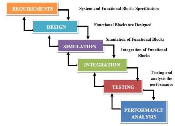
Fig. 2. Waterfall Methodology with Loopback
5. SA-I Afferent Circuit
In the SA-I circuit, a spike train is generated when force is applied to the sensor. SA-I afferents exhibit spike adaptation. “Fig 3” shows the Block Diagram of SA- I Afferent Circuit. The spiking rate is proportional to the force amplitude. SA-I consists of an inverting differentiator, integrator, Schmitt trigger, current mirrors, logic gates, and a LIF neuron circuit. A single-stage differential amplifier along with a capacitor and resistor are used to implement the differentiator circuit. The output signal of the differentiator circuit is given by equation (1)
_
-
^d^d
where
^sensor dt
+ Vd c
r dd d c = 9
In the above “Equation 1” the values of and are selected in such a way that it satisfies the time constant to match the biological signals. A low-power CMOS Schmitt trigger circuit is used to differentiate the positive and negative slopes of the sensor output. The output goes high for a positive edge and remains high until a negative edge occurs. The lower and upper trigger values are set to 0.8V and 1V. A CMOS inverter is used so that the control signal is inverted. An integrator circuit is also used to control the current flowing in the neuron circuit. The time constant for the integrator and differentiator circuits is of the order of several milliseconds. Two transistors are used to adjust the neuron input current. When the output of the Schmitt trigger is high, the transistor is ON and activates the neuron circuit to produce spiking responses. If is OFF, the neuron does not fire. The gate voltage of the transistor is proportional to the integrator‘s output. During the active time interval, integrator output increases and the spiking frequency of the neuron decreases. The integrator output is given by “equation (2)”,
∫ Vint = [ ∫ ^sensor dt
The current for transistor Tr1 is calculated from the MOSFET saturation current “equation (3)”, hrl = (7) VDD
-
Vint
-
| ^tp |2
In the “equation 3” the transistor ^VL is in the saturation region when it is active. The SA-I afferent circuit consists of SA-I afferents. SA-I afferents are responsible for sustaining mechanical stimulation. When an object indents the eskin sensor, the SA-I afferents generate electrical impulses or spikes in their activity. The frequency of spikes generated by these afferents correlates with the magnitude of force applied to the sensor. The adaptation of SA-I afferents enables the sensory fibers to differentiate between tactile and sustained stimuli. When a more vital indentation occurs, the SA-I afferents respond with a higher spike frequency, providing rapid and robust signaling about the initial force applied to the e-skin sensor. As the indentation continues, the firing rate adapts or decreases over time, conveying information about the duration and sustained nature of the applied force.
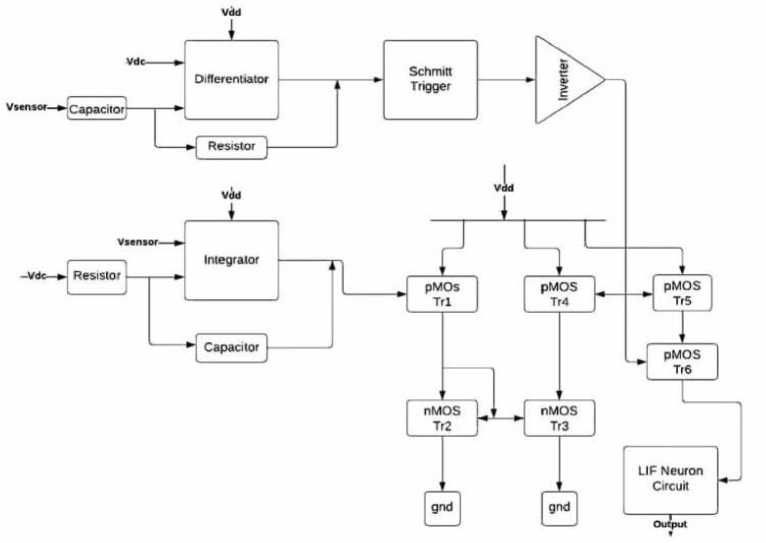
Fig. 3. Block Diagram of SA- I Afferent Circuit
-
5.1 Differentiator
The op-amp-based differentiator circuit consists of an operational amplifier, a resistor (R), and a capacitor (C) connected in a specific configuration. The input voltage ( Vi ) is applied to the inverting terminal of the op-amp, and the output voltage ( к ) is taken from the output terminal. Using the nodal analysis technique, we can derive the relationship between the input and output voltages in the op-amp differentiator circuit are as shown in “Fig 4”. Considering the voltage at the inverting input terminal as zero volts, we can write the nodal “equation 4” at that node as follows:
-С d( dt)+0- =0 (4)
Simplifying the “equation 5”, we get:
-С d ( dt)=T (5)
Solving for ^0 , we find:
dV;
V□ =-RCd( )
When RC = 1 second, the output voltage ( ^o) can be expressed as:
dvi
dt
The output voltage ( К ) of the op-amp-based differentiator circuit is directly proportional to the derivative of the input voltage (к) with respect to time. Thus, the circuit acts as a differentiator, providing an output that represents the rate of change of the input signal.
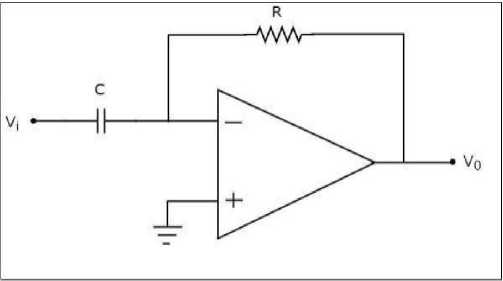
Fig. 4. Op amp-based differentiator
The differentiator circuit is a fundamental component within the biomimetic SA-I afferent circuit that is specifically designed to process the input signal from the sensor in a precise and accurate manner. Its primary purpose is to calculate the derivative of the input signal, which represents the rate of change of the sensor's output voltage over time. This circuit employs a single-stage differential amplifier in combination with a capacitor ( ^d ) and a resistor ( Rd ) to perform the differentiation operation. The output signal of the differentiator circuit, denoted as _ , is determined by the “equation (1)”:
^iff _
- Rd^d
^sensor dt
+ VdC
where
=
^dc represents a voltage bias typically set at half of the supply voltage ( Vdd ) as shown in the equation 8 The selection of appropriate values for Rd and Cd is crucial to ensure that the time constant of the differentiator circuit matches the characteristic time constant of the biological signals being processed. This accurate differentiation operation allows the circuit to capture the dynamic aspects of the sensor's response to applied forces, providing detailed information about the force magnitude and the rate of change. Incorporating the differentiator circuit within the SA-I afferent circuit, it contributes to the generation of spiking responses that closely mimic the behavior of natural SA-I afferents, enabling users to perceive and respond to various tactile stimuli with enhanced precision and realism.
-
5.2 Schmitt Trigger
The CMOS Schmitt trigger circuit utilizes the properties of CMOS technology to achieve the hysteresis effect. It typically consists of a voltage divider network, two cross-coupled inverters, and feedback resistors. The voltage divider network sets the threshold levels for the switching operation.
Operation:
-
i. Initial State: Assume that the output of the Schmitt trigger is initially at a low logic level (0) and the input voltage is increasing. Rising Threshold (Upper Threshold): As the input voltage rises, it reaches a specific threshold level determined by the voltage divider network. At this point, the first inverter, connected to the input, begins to change its output from low to high (1).
-
ii. Positive Feedback: The high output from the first inverter is cross-coupled to the second inverter's input. This positive feedback reinforces the switching action and ensures a quick transition to a high logic level at the output.
-
iii. Stable State (High Output): Once the output reaches a high logic level, the input voltage can decrease without affecting the output. This is because the second inverter, receiving a high input, will maintain its output at a low logic level, thanks to the cross-coupling.
-
iv. Falling Threshold (Lower Threshold): As the input voltage continues to decrease, it eventually reaches a lower threshold level determined by the voltage divider network. At this point, the second inverter starts changing its output from low to high (1).
-
v. Negative Feedback: The high output from the second inverter is cross-coupled to the first inverter's input, creating negative feedback. This reinforces the switching action in the opposite direction, ensuring a quick transition to a low logic level at the output.
-
vi. Stable State (Low Output): Once the output reaches a low logic level, the input voltage can increase without affecting the output. The first inverter, receiving a low input, will maintain its output at a high logic level due to the cross-coupling.
-
5.3 Integrator
The Schmitt trigger circuit plays a crucial role within the proposed biomimetic circuit for electronic skin with application in hand prostheses. This circuit is responsible for differentiating the positive and negative slopes of the sensor's output signal, enabling reliable detection of edges and transitions. The Schmitt trigger operates as a comparator with hysteresis, which ensures stable switching behavior and noise tolerance. In the context of the SA-I afferent circuit, the Schmitt trigger circuit distinguishes between positive and negative edges, indicating significant indentation and release of applied force, respectively. When a positive edge is detected, the Schmitt trigger's output goes high and remains high until a negative edge is encountered. The lower and upper trigger values are carefully set to appropriate voltage thresholds, typically around 0.8V and 1V, respectively as shown in below “equation 8”.
If
_ > 1V, sch = 0 → Transistor Tre is ON
_ < 0.8V, ^sch = → Transistor Tre is OFF (8)
The output of the Schmitt trigger circuit serves as a control signal for activating the subsequent neuron circuit in the SA-I afferent circuit. By incorporating the Schmitt trigger circuit, the biomimetic circuit closely replicates the behavior of natural SA-I afferents, enabling users of hand prostheses to receive realistic and intuitive sensory feedback, particularly in response to tactile stimuli.
The op-amp-based integrator circuit is as shown in “Fig 5” consists of an operational amplifier, a resistor (R), and a capacitor (C) connected in a specific configuration. The input voltage (Vi) is applied to the inverting terminal of the opamp, and the output voltage (Vo) is taken from the output terminal. Using the nodal analysis technique, we can derive the relationship between the input and output voltages in the op-amp integrator circuit.
Considering the voltage at the inverting input terminal as zero volts (virtual short concept), we can write the nodal “equation (9)” at that node as follows:
0- +Cd( dt)=0
Simplifying the “equation (10)”, we get:
-7=Cd( dt )
Rearranging the “equation (11)”, we find:
( dVo)=-Л
V dt / RC
Integrating both sides of the “equation (12)”, we have:
∫dVa = ∫(-RC)dt
Integrating, we get:
V =- ∫V i dt
When RC = 1 second, the output voltage ( к) can be expressed as:
V □ =-∫V i dt
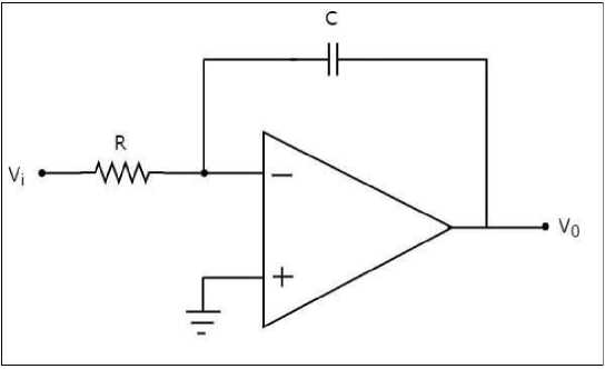
Fig. 5. Op-amp based integrator circuit
Integrator‘s primary function is to integrate the input signal from the sensor over time, providing an accumulated representation of the applied force. The integrator circuit plays a vital role in generating a slowly varying signal that is proportional to the force applied to the sensor. This is achieved through the integration process, which sums up the input signal's values over time. The output of the integrator circuit, denoted as Vint , is calculated by integrating the sensor's output voltage over time, with Rt and Cr representing the resistor and capacitor values chosen to achieve the desired time constant. The integrator output is given by
1 г
Vin t = [J vsensordt ]
The integration time constant is carefully selected to match the characteristic time constant of the SA-I afferents, ensuring an accurate representation of sustained forces. The slowly varying signal produced by the integrator circuit provides valuable information about the duration and sustained nature of the applied force. By adjusting the current flowing in the subsequent neuron circuit based on the integrator's output, the spiking frequency of the neuron circuit can be modulated, allowing users to perceive and interpret the force dynamics more effectively. The integrator circuit's role in the biomimetic circuit enables users of hand prostheses to experience a more natural and intuitive sensory feedback, enhancing their ability to interact with objects and the environment.
-
5.4 Role of current mirrors and logic gates
-
5.5 Leaky Integrate and Fire Neuron (LIF) Circuit
The role of current mirrors and logic gates in the biomimetic circuit for electronic skin is crucial for ensuring proper signal processing and control of the circuit's functionality. These components play key roles in shaping the input and output signals, enabling the circuit to emulate the behavior of tactile afferents effectively.
Current mirrors are fundamental building blocks in analog circuits and serve the purpose of replicating and mirroring currents in a circuit. In the biomimetic circuit, current mirrors are used to control the current flowing through the neuron circuit, which directly affects the spiking responses. By adjusting the current through the transistor in the current mirror configuration, the firing rate and response characteristics of the circuit can be modulated. This modulation enables the circuit to generate spiking responses that are proportional to the force or indentation depth sensed by the electronic skin.
Logic gates, on the other hand, are used to control the activation and deactivation of certain circuit components based on specific conditions. In the biomimetic circuit, logic gates are employed to determine whether the neuron circuit should fire or remain inactive. The output of the Schmitt trigger, which detects the positive and negative slopes of the sensor output, is fed into a logic gate. When the output of the Schmitt trigger is high, indicating the presence of a tactile stimulus, the logic gate activates the neuron circuit, resulting in spiking responses. Conversely, if the output of the Schmitt trigger is low, the logic gate keeps the neuron circuit deactivated, preventing spiking responses. This mechanism allows the circuit to produce spiking activity only in the presence of significant tactile stimulation, mimicking the behavior of SA-I afferents. The proper integration and utilization of current mirrors and logic gates ensure the accurate and reliable operation of the biomimetic circuit. By manipulating the currents and controlling the activation of circuit components, these elements contribute to the faithful replication of the behavior of tactile afferents. Their role in shaping the input signals, processing the signals, and determining the output responses is crucial for providing realistic sensory feedback in prosthetic hand applications.
The leaky integrate-and-fire (LIF) neuron circuit is a commonly used model in spiking neural networks, designed to mimic the behavior of biological neurons. This circuit is capable of converting analog input currents into output spike trains, which are the fundamental units of communication in neural systems “Ref. [28]”.
The behavior of the LIF neuron circuit is governed by the following differential “equation 16”:
тт (jU) =-(и - u e q) + RI (16)
In this equation, u represents the membrane potential of the neuron, and иeq is the equilibrium potential. тт refers to the membrane time constant, which determines the rate at which the membrane potential changes. The right-hand side of the equation consists of two terms: the first term represents the leakage of the membrane potential towards the equilibrium potential, and the second term represents the contribution of the input current.
When the membrane potential u crosses a threshold voltage uth, the neuron generates a spike, and the membrane potential is reset to the equilibrium potential. The LIF neuron circuit incorporates various sections to perform the leaky integration and spike generation processes. The input current, denoted as Ineuron, is injected into the leaky integrator section via a current mirror. The leaky integrator is implemented using a capacitor (C) for integration and a transistor for controlling the leakage. The transistor provides a variable conductance, allowing the stored charge on the capacitor to leak away gradually.
The leaky integrator section integrates the injected current over time using the capacitor and controls the leakage through the transistor. This process emulates the gradual leakage observed in biological neurons. The integrated potential is then compared to a threshold voltage using a Schmitt trigger, which detects when the potential crosses the threshold and generates an output spike.
Following the generation of a spike, the reset section of the circuit ensures that the membrane potential is reset to the equilibrium potential ( ue q ). The buffer section amplifies and isolates the spike signal for further processing or transmission. The LIF neuron circuit is characterized by its ability to process both excitatory and inhibitory input signals, allowing it to emulate the behavior of biological neurons accurately. The circuit parameters, such as the capacitance ( Cu ), supply voltage ( Удд ), and bias voltage ( Vb ), are crucial in determining the circuit's performance and behavior.
-
5.6 Implementation
Circuit simulation plays a crucial role in the development of electronic skin (e-skin) technologies, particularly in the design and optimization of biomimetic circuits. It allows researchers and engineers to evaluate the performance, functionality, and behavior of the circuit before its physical implementation. Circuit simulation provides a cost-effective and efficient means to assess the circuit's operation, validate its design choices, and identify potential issues or limitations.
In the context of e-skin development, circuit simulation allows for a comprehensive analysis of how the biomimetic circuit interacts with the sensor inputs and generates appropriate outputs. By mimicking the behavior of tactile afferents, the circuit should accurately respond to different levels of force, indentation, and other tactile stimuli. Through simulation, engineers can observe the circuit's response characteristics, such as spiking rates, adaptation properties, and dynamic range, under various input conditions. This enables fine-tuning and optimization of the circuit design to achieve the desired performance and functionality.
Moreover, circuit simulation enables a deeper understanding of the circuit's behavior and its relationship with the underlying biological principles. By comparing simulation results with known physiological responses of cutaneous mechanoreceptors, researchers can validate the biomimetic circuit's ability to replicate the sensory processing of tactile afferents. This alignment with biological principles is essential for creating e-skins that provide realistic and intuitive sensory feedback to users. The utilization of Cadence Virtuoso software is of paramount importance in the design and implementation of the proposed biomimetic circuit for electronic skin, specifically tailored for hand prostheses. As a widely used electronic design automation (EDA) tool, Cadence Virtuoso provides advanced capabilities for designing and simulating complex integrated circuits.
The software enables us to design the different components of the circuit like a differentiator, integrator, Schmitt trigger, logic gates, etc. Cadence Virtuoso also enables us to simulate the behavior of the designed circuitry. Through various simulation options, such as transient analysis, frequency-domain analysis, and parameter sweeps, the software allows for thorough testing and verification of the circuit's functionality. It helps ensure that the circuit operates as intended and accurately mimics the behavior of SA-I afferents. The software's optimization capabilities are valuable in refining the circuit design as shown in “Fig 6”.
The simulation parameters and optimization techniques in Cadence Virtuoso software are instrumental in validating the biomimetic circuit's behavior, fine-tuning its design, and optimizing its performance for electronic skin applications. Its powerful features and capabilities enable engineers to create and validate complex circuitry, ensuring the successful development of the proposed electronic skin technology.
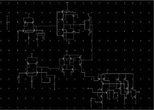
Fig. 6. Implementation of SA-I afferent circuit in Cadence Virtuoso
-
5.7 Extension
Cadence Virtuoso is a widely used Electronic Design Automation (EDA) software suite developed by Cadence Design Systems. It is primarily employed for designing and simulating integrated circuits (ICs) and semiconductor devices. Virtuoso offers a comprehensive set of tools that facilitate the design, verification, and manufacturing of complex ICs.
Key features of Cadence Virtuoso:
Schematic Editor: Virtuoso provides an intuitive and powerful schematic editor, enabling engineers to create electronic circuit schematics using a wide range of components and design rules.
The Schematic Editor includes the following features:
Circuit Creation, Wiring and Connectivity, Symbol Editing, Hierarchical Design, Design Rule Checking (DRC), Parameterized Components, Annotation and Documentation, Simulation Setup, and Integration with Layout Editor.
Layout Editor: The layout editor in Virtuoso allows users to draw physical layouts of the integrated circuits, ensuring that the final design is manufacturable and meets the required specifications. The Layout Editor is a critical stage in the IC design process, as it defines the physical representation of the circuit, which is ultimately used in the semiconductor fabrication process. Its capabilities play a key role in ensuring a successful design that meets manufacturing requirements and achieves optimal performance.
Simulation: Virtuoso supports various simulation methods, including analog, digital, mixed-signal, and RF simulations. Engineers can verify the functionality and performance of their designs through transient, frequencydomain, and other types of analysis.
Virtuoso supports various types of simulations, including
Analog Simulation: Used for analyzing continuous-time and continuous-value circuits, such as amplifiers, filters, and oscillators.
Digital Simulation: Analyzes digital circuits, including logic gates, flip-flops, and other digital components.
Mixed-Signal Simulation: Simultaneously analyzes both analog and digital parts of a mixed-signal circuit, often found in systems-on-chip (SoCs).
RF Simulation: Specifically tailored for high-frequency circuits like RF amplifiers, mixers, and filters.
By performing various types of simulations, designers can gain valuable insights into the behavior of biomimetic circuits and make informed design decisions to achieve optimal performance and reliability.
A layout is a visual representation of an integrated circuit, depicted using planar geometric shapes such as rectangles and polygons. It serves to illustrate the precise patterns of metal, polysilicon, oxide, or diffusion layers that form the circuit's essential components, including resistors, inductors, capacitors, and transistors.
Working with standard processes like 45nm, 90nm, or 180nm available in our lab, the final behavior of the integrated circuit is significantly influenced by the arrangement and connections of these geometric shapes. These configurations contribute to parasitic resistances and capacitances, which can have a notable impact on the circuit's overall performance. Hence, during the layout design phase, the designer must meticulously consider critical performance metrics, such as the power-delay product and chip size, while optimizing to meet specific criteria and design goals.
During the design of digital circuits, engineers typically adhere to an ASIC (Application-Specific Integrated Circuit) design flow. This approach involves utilizing standard cells, where the height remains consistent across the entire cell library. However, to accommodate different logical functions and drive strengths, the widths of these standard cells vary accordingly. The “Fig 7” illustrates the generalized concept of standard cell height in such design methodologies.
VDD BUS
P-TYPE TRANSISTORS
DIFFUSION SPACING
N-TYPE TRANSISTORS
GNDBUS
Cell Height
-
Fig. 7. Standard Cell Height
Design Rule Checking (DRC): The layout will be examined against specific design rules and guidelines to identify any violations.
Layout design using Virtuoso Layout Suite L Editor
-
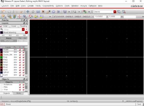
i. To access Virtuoso Layout Suite L Editor, begin by opening the Command Interpreter Window (CIW) and then proceed to select "File" from the menu, followed by "New" and "Cellview." This action will trigger the appearance of the 'New File' form, where you should input the required details as shown in the accompanying figure.
Cell: SAafferent11View: Layout
Once the information is filled in, click on the OK button to proceed. This action will initiate theopening of the layout view for the cell named "INVX1" in the Virtuoso Layout Suite L Editor.
-
ii. Upon launching Virtuoso Layout Suite L Editor is as shown in “Fig 8”, the corresponding window will be displayed on the screen.
-
Fig. 8. Layout Editor
The left side of the window contains a panel named 'Layers,' which is organized into three primary categories: layer color, layer name, and layer purpose. Each category provides specific details and information about the layers used in the layout. The table below outlines the details and descriptions of each layer in the 'Layers' panel is as shown in below “Table 1”.
Table 1. Details and descriptions of each layer in the –Layers panel
|
Color |
Matches the color in the Editing window.Each layer has its own color and pattern. |
|
Name |
The type of layer (Nwell, oxide, poly, etc) |
|
Purpose |
Drawing is used in layout, slot is used tocreate a hole for metal stress relief |
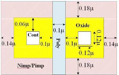
To design an NMOS transistor, specific rules must be followed for each layer as shown in fig 9. Here is a summary of the rules related to the NMOS transistor:
Oxide Layer: The oxide layer is used for isolating different components on the integrated circuit. The minimum oxide width must be greater than or equal to a certain value to ensure proper isolation.
Nimp Layer: The Nimp (N-type implant) layer is essential for creating the source and drain regions of the NMOS transistor. The minimum Nimp width needs to meet the design requirements for proper doping levels.
Cont Layer: The Cont (Contact) layer is responsible for connecting the transistor's source and drain regions to the metal layers. Proper alignment and minimum spacing rules must be followed for reliable connections.
Poly Layer: The Poly (Polysilicon) layer forms the gate of the NMOS transistor. The minimum Poly width and spacing must be observed to achieve the desired gate length and ensure proper transistor behavior.
The following figure illustrates some of the design rules mentioned above:
-
Fig. 9. Design Rules for layers
In the GPDK 90 nm Mixed Signal Process Spec, the PMOS transistor structure comprises five main layers:
Oxide, Poly, Pimp, Cont, and Nwell. To design a PMOS transistor, each layer must follow specific rules. The rules related to the PMOS transistor are similar to those of the NMOS, with the addition of the Nwell layer, which has its own set of rules as follows:
-
1) Oxide Layer: The Oxide layer is used for isolation purposes, ensuring proper separation between different components on the integrated circuit. The minimum width of the Oxide layer must meet the specified requirements for effective isolation.
-
2) Poly Layer: The Poly layer forms the gate of the PMOS transistor. Similar to the NMOS, the minimum Poly width, and spacing must be adhered to in order to achieve the desired gate length and ensure proper transistor behavior.
-
3) Pimp Layer: The Pimp (P-type implant) layer is responsible for creating the source and drain regions of the PMOS transistor. The minimum Pimp width should be designed to meet the desired doping levels.
-
4) Cont Layer: The Cont (Contact) layer is essential for connecting the PMOS transistor's source and drain regions to the metal layers. Proper alignment and minimum spacing rules must be followed for reliable connections.
-
5) Nwell Layer: The Nwell layer is an additional layer specific to PMOS transistors. It is used to create the substrate for the PMOS transistor. The rules for the Nwell layer are defined to ensure proper substrate doping and isolation.
-
iii. To establish the necessary connections in the layout, we need to connect the drain regions of both NMOS and PMOS transistors. Additionally, we must connect the sources of both MOS devices to their respective body terminals.
To achieve these connections, we will use the 'Metal1 (drw)' layer. This layer will be utilized to connect the drain regions of both NMOS and PMOS transistors. It will also be employed to establish connections between the sources of the MOS devices and their corresponding body terminals.
By accurately implementing these connections using the 'Metal1 (drw)' layer, we can ensure proper functionality and signal flow in the integrated circuit design, creating a well-organized and efficient layout for both NMOS and PMOS transistors.
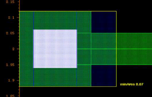
Also draw a ‗Metal1 (drw)‘ rectangle on the via is as shown in below “Fig 10”, because the default Metal1 rectangle area is less than the required minimum.
-
Fig. 10. Via on the metal
-
iv. For the 'in' pin, 'vdd!', and 'gnd!', select 'input' as the 'I/O type.' For the 'out' pin, choose 'output' as the'I/O type.'
By accurately creating these pin connections using the appropriate layers, we can ensure proper signal routing and connectivity for vdd!, gnd!, in, and out signals in the layout design.
-
v. The final layout will look as shown in “Fig 11”.
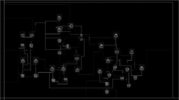
Fig. 11. Final Layout
6. Results
This work is implemented using Cadence Virtuoso. Following are the results of the signals generated when the simulation is done.
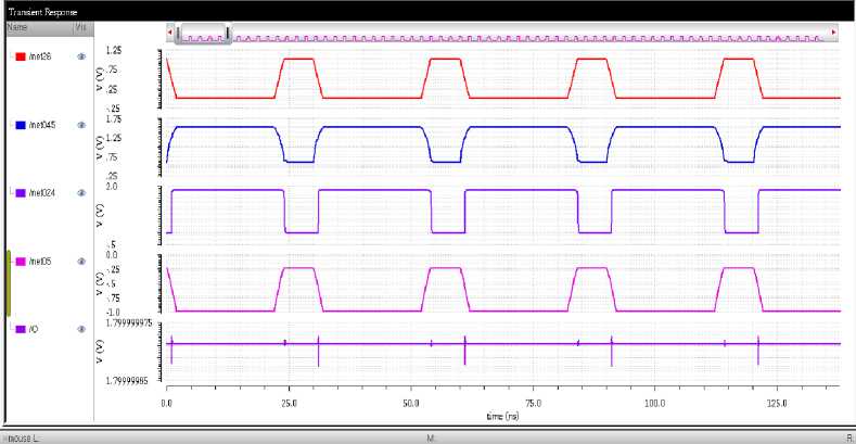
Fig. 12. Illustration of Different Stages Output for SA-I Circuit
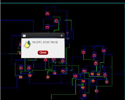
Fig. 13. DRC check for the layout
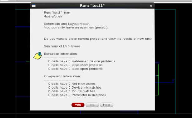
Fig. 14. LVS check
7. Discussion
Illustration of different stages of SA-I afferent circuit which includes waveform of (a) The first waveform indicates the ^sensor input. (b) Expected output from the differentiator circuit indicating the derivative of the sensor output voltage. It has an amplitude of up to1.522v (c) The output voltage of the Schmitt trigger of amplitude up to1.7983v (d)The output of the integrator circuit. It integrates the ^sensor . (e)The spikes generated from the LIF neuron circuit in response to the input is as shown in “Fig 12”.
The indentation stimulus profile, which has onset, hold, and offset phases, is applied to the sensor. The predicted output of the differentiator circuit, which is the derivative of the sensor output voltage at the offset phase output will be Vdd .t he s chmitt trigger circuit converts the analog emg signals or other input signals into digital signals with well-defined thresholds. Its output is a binary signal, which is high (1) when the input exceeds the higher threshold and low (0) when it goes below the lower threshold. The integrator circuit takes the differentiated EMG signal (from the differentiator) as input and performs the mathematical operation of integration. The output is the integral of the differentiated EMG signal with respect to time. The output of the integrator circuit that computes the ^sensor integral. The LIF circuit models the behavior of neurons in the brain. Its output represents the activity of the neuron in response to the integrated input signal, typically in the form of action potentials (spikes) when a certain thresholdis reached.
These outputs are essential indicators of the circuit's functionality and performance. The 0.25V amplitude from the integrator suggests that the circuit is effectively providing a slowly varying signal, proportional to the force applied to the sensor, which is a key characteristic of SA-I afferents in the human sensory system. On the other hand, the 1.5V amplitude from the differentiator implies that the circuit is efficiently capturing the dynamics of the SA-I afferent response to sustained indentation, showcasing its ability to detect changes in indentation depth.
Finally, the generation of output spike signals at the output of the LIF neuron circuit demonstrates successful replication of the neural behavior observed in SA-I afferents. The firing of spikes corresponds to the generation of electrical impulses in response to mechanical stimuli, further confirming the biomimetic nature of the circuit. “Fig 13” shows the DRC check for the Layout, and “Fig 14” shows the LVS check for the layout.
8. Conclusion
In conclusion, this work introduces a biomimetic circuit designed to replicate the behavior of slowly adapting (SAI) afferents, crucial for encoding sustained indentation and providing essential sensory feedback in upper limb prostheses. The circuit was meticulously designed and simulated using Cadence Virtuoso software, a powerful tool for circuit design and optimization, in the extension the schematic and layout of the circuit is designed. The results of the simulation, based on a grid of mechanoreceptors providing realistic inputs, demonstrated that the biomimetic circuit successfully emulates the response of SA-I afferents to sustained indentation. The circuit exhibited a slowly adapting discharge that linearly correlates with the depth of indentation, representing a significant advancement in providing sensory feedback for upper limb prostheses.
The proposed biomimetic circuit offers great promise in addressing the crucial need for sensory feedback in upper limb prosthetics. By integrating this circuit into upper limb prostheses, amputees can experience more intuitive and realistic sensations during interactions with their environment. The ability to replicate SA-I afferent behavior provides users with vital information about the magnitude and duration of applied forces, thereby enhancing their overall perception and control of the prosthesis. The findings of this study contribute significantly to the field of prosthetics, particularly in the development of more advanced and sophisticated upper limb prostheses. The successful implementation and simulation of the biomimetic circuit demonstrate its potential as a viable solution for providing amputees with enhanced sensory feedback, ultimately leading to an improved quality of life and seamless reintegration into daily activities.
9. Future Scope
The successful development of the Biomimetic circuit for electronic skin with application in hand prostheses opens up exciting possibilities for future advancements in the field of prosthetics and sensory feedback. Here are some potential future directions and opportunities for further exploration:
-
i. Enhanced Sensory Resolution: Continued research can focus on improving the resolution and fidelity of sensory feedback provided by the biomimetic circuit. This could involve fine-tuning the circuit design parameters, optimizing the integration of additional sensor types, or exploring novel methods for signal processing and interpretation.
-
ii. Multimodal Sensory Integration: Integrating multiple sensory modalities, such as touch, temperature, and proprioception, into the electronic skin and prosthetic devices can provide a more comprehensive sensory experience. Future work can investigate the integration of additional sensor types and the development of circuitry capable of processing and integrating multiple sensory inputs.
-
iii. Adaptive and Learning Systems: Building on the concept of biomimicry, future developments could focus on creating adaptive and learning systems within the electronic skin. These systems could adapt to individual users' needs and preferences, dynamically adjusting the sensitivity and response characteristics of the circuitry to optimize sensory feedback.
-
iv. Wireless and Miniaturized Designs: Shrinking the size and integrating wireless communication capabilities into the electronic skin and prostheses would enhance user comfort, portability, and ease of use. Future efforts can focus on developing miniaturized and energy-efficient designs that allow seamless integration with prosthetic limbs.
-
v. Clinical Applications and User Trials: Conducting comprehensive user trials and clinical studies to evaluate the effectiveness and user experience of the biomimetic circuit in realworld settings is crucial. Future research can involve collaborating with medical professionals and prosthesis users to validate the circuit's performance and gather valuable feedback for further refinement.
Acknowledgment
The satisfaction and euphoria that accompany the successful completion of my project work would be incomplete unless I mention the names of people who made it possible and whose guidance and encouragement served as a beacon light to my efforts with success. It gives me immense pleasure to acknowledge and express my deepest gratitude to all who helped me throughout my project work.
First and foremost, I owe a special heartfelt gratitude to my guide Dr. PunithKumar M B, Professor of Electronics and Communication Engineering, P.E.S College of Engineering, Mandya, for his able guidance, concern, inspiration, and constant support that needed throughout this project work.
I am thankful to all staff of Department of Electronics and Communication Engineering,P.E.S College of Engineering, Mandya, for their constant support and encouragement.
I am grateful to my parents, friends and to those who have directly or indirectly helped me in completing the project successfully.
