Design of 12B/14B: A Novel SERDES Encoding Technique

Автор: Ashok Kumar, Sanjeev Mehta
Журнал: International Journal of Information Technology and Computer Science(IJITCS) @ijitcs
Статья в выпуске: 9 Vol. 6, 2014 года.
Бесплатный доступ
In satellite systems, large amount of high speed data is required to be transmitted from one system to another. Conventional parallel data transmission requires a large number of cables/interface-packages and results in large weight and volume. Parallel interface in a typical future camera system requires >8000 cables between camera electronics and data handling system. In addition, with increase in transmission rate, problems associated with crosstalk become more critical. One possible solution identified is serial interface, also termed as SERDES (SERializer/DESerializer) interface. A typical SERDES interface comprises of encoder/decoder, PLL, timing-control and multiplexer/de-multiplexer. Encoding of serial data solves high speed serial data transmission problems by incorporating clock embedding, DC balancing, sync info insertion and error detection. DC balancing also solves the issue of Inter-Symbol Interference (ISI). Available SERDES interface devices have limitations like poor reduction factor, no clock embedding or non-availability of space qualified part. Hence, an attempt is made to understand and implement SERDES encoder/decoder with a goal of indigenous SERDES ASIC development. Due to 12-bit input interface, a novel 12B/14B encoding technique is designed and developed. The developed technique preserves many good properties widely used 8B/10B encoding technique. FPGA simulation results achieved >50MSPS parallel rate which will lead to >700 Mpbs serial rate. Developed technique is very efficient and suitable for onboard implementation.
SERDES, BER, 8B/10B, Disparity, DC-balance, AC-coupled, Run-length
Короткий адрес: https://sciup.org/15012152
IDR: 15012152
Текст научной статьи Design of 12B/14B: A Novel SERDES Encoding Technique
Published Online August 2014 in MECS
Today, a typical remote sensing camera requires processing of multiple video ports. Each port is being processed to yield typically ≥7-bit digitized video data, which needs to be transmitted to other subsystems for further processing/transmission. This is conventionally done using multiple cables (parallel data transmission). Increase in number of video ports increases weight, volume and power requirements. Table-1 shows comparison of detector data parallel interface (digitized CCD video data between camera electronics and data handling system) requirement of a typical previous and future missions.
With increase in transmission rates, problems associated with crosstalk start to become more critical. One possible solution to this problem is serial transmission i.e. to perform parallel-to-serial conversion at the transmitter end, transmit the serial stream preferably over a differential medium and convert the serial data back to parallel form at the receiver end. This interface is also termed as SERDES (SERializer at transmitter end / DESerializer at receiver end). It considerably reduces the number of interconnecting signals and overcomes the issues of crosstalk.
Table 1. Comparison of Interface Requirements
|
Missions/ Parameters |
Previous Missions |
Future Missions |
|
Sampling Rate (MSPS) |
4.2 |
10 |
|
Video Ports |
16 |
384 |
|
Interfaces |
320 |
8448 |
|
Interface Power (W) |
1.5 |
90.3 |
|
Harness Weight (excl. connector) (Kg) |
3.6 |
94.1 |
So, for high resolution electro-optical cameras, SERDES interface is a suitable candidate for communication between two sub-systems. Off the shelf SERDES devices [1] are available from few vendors. They have limitations like poor reduction factor, no clock embedding or non-availability in required operating frequency range. Most of these available devices operate in excess of >1Gbps with their patented design. Information of internal functional blocks is not available, which is required from reliability point of view. In addition, costs are on higher side and non-availability as space qualified part may hamper project schedule.
Hence, indigenous ASIC development is planned for SERDES interface. SERDES is a very complex device, which has encoder/decoder, PLL, timing-logic, clock and data recovery, LVDS block etc [2]. Encoder/decoder is one of the most critical design blocks as it provides preemphasis to media losses. Hence, as an initial step towards ASIC development, an attempt is made to understand and implement encoder/decoder blocks. Various SERDES encoding techniques are surveyed first. 8B/10B [3-6] is one of the best line encoding technique, which is used in 1GbE standard. Only issue with this technique is its byte oriented nature. For 12-bit satellite systems, it has to be implemented as two separate 8B/10B
SERDES, which produce 8 overhead bits (40%). Hence, for optimum use of channel bandwidth, new coding technique 12B/14B is developed and proposed. It preserves many good code properties of the 8B/10B. This paper presents theoretical background, design principles, performance characteristics and implementation aspects of this new encoding technique. Initially demonstration of performance using FPGA is considered.
-
II. Encoding Technique’S Properties And Their Survey
Basic functional block diagram of SERDES architecture is shown in Fig. 1. Main components of Serializer are encoder, PLL, control logic and multiplexer. Main components for deserializer are clock-data recovery (CDR), word synchronizer, and decoder and control logic.
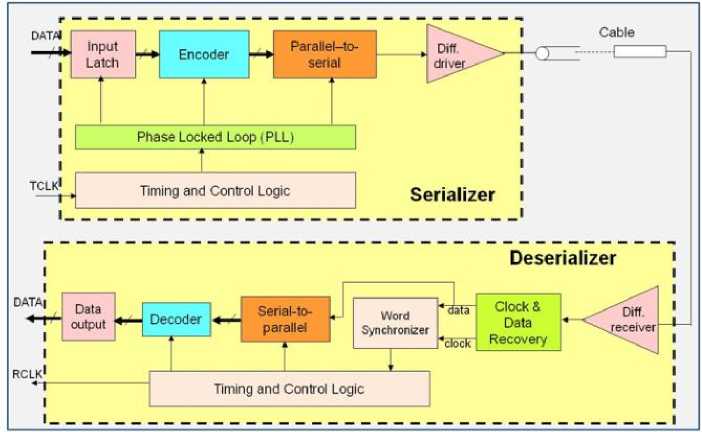
Fig. 1. Block Diagram of SERDES Architecture
The main requirements to be fulfilled by encoder are minimum Inter Symbol Interference (ISI) in the serial stream; suitability for AC coupled application, embedded clock information. These goals can be achieved with the following properties in the encoded data:
-
A. DC Balancing
A DC balanced serial data means that it has zero disparity, where disparity means difference in number of ones and zeros in a block of code (e.g. for code 11010101, disparity = +2). Hence, DC balancing requires sufficient data transitions which are incorporated intentionally through encoding. This property ensures that charge build-up is avoided in the transmission medium; making it suitable for AC coupled applications. DC balancing also reduces ISI. Effect of DC balancing is shown in Fig. 2, where many consecutive ones forces bit loss at transition.
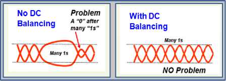
Fig. 2. Effect of DC Balancing
-
B. Small run-length
It is defined as the maximum number of contiguous zeros or ones possible in the serial data stream. It is also related with DC balancing. A small run-length data stream provides data transitions within a small length of data, which are mandate requirement for serial clock recovery from data stream. This also limits the spectral content of the serial stream that can ease the task of suppressing electromagnetic radiation. For example, given a 1 Gbps line rate after 8B/10B coding, the maximum and minimum 1st harmonic frequencies are 500 MHz and (500 MHz)/5 = 100 MHz. Hence, frequency spectra below 100 MHz could be suppressed.
-
C. Predefined control characters for synchronization
Such characters must be singular i.e. they must not appear in any sequence of valid data bits including overlapped data characters. These control characters are required to define word boundaries (i.e. locating LSB and MSB position of a word in serial data stream).
-
D. Error detection
Error detection combats the data loss in transmission. Encoding technique should detect single/multiple bit errors, if possible.
-
E. Minimum overhead bits
Encoding technique should incorporate minimum overhead bits to ensure maximum usage cable bandwidth.
Comparison of various standard encoding techniques [7] w.r.t. above mentioned parameters is given in Table-2. The performance of these encoding schemes with respect to transition density, DC balance and output data rate is detrimental in selecting the best method for SERDES application.
Table 2. Comparison of SERDES Encoding Techniques
|
Encoding Technique |
High transition Density |
DC Balance |
Effect on Data rate |
Remarks |
|
NRZ |
X |
X |
None |
Simple |
|
RZ |
√ |
X |
Increases by 100% |
Simple |
|
AMI |
X |
X |
None |
Simple |
|
Manchester Phase |
√ |
√ |
Increases by 100% |
- |
|
8B/6T |
√ |
√ |
Reduces |
Not suitable beyond 30MHz |
|
PAM-5 |
√ |
√ |
Reduces |
susceptible to noise |
|
8B/10B |
√ |
√ |
Increases by 25% |
Byte oriented |
As can be seen from the Table-2, NRZ, RZ and AMI schemes do not provide DC balancing. Multi-level schemes like 8B/6T are complex to design and susceptible to noise. The Manchester phase encoding has implication of 100 % overhead bits, however it provide very good transition density and DC balancing.
Based on the above comparison, it is seen that 8B/10B [3-6] encoding is the most suitable technique for high speed serial transmission. Some of the properties of 8B/10B are summarized below:
-
• It guarantees transition density of at least 30 transitions per 100 bits.
-
• It provides DC balance property, with disparity (difference between total number of ones and zeros for a given length) staying within +/-2. It guarantees a maximum run-length of 5 for encoded data.
-
• It contains singular control characters.
-
• It can detect all single-bit and some multiple-bit errors because many of the 10-bit code permutations are not valid.
Due to these reasons, many standards such as PCI Express, IEEE1394b, Serial ATA, Fiber Channel, Gigabit Ethernet, InfiniBand, XAUI, Serial RapidIO, DVB, HDMI and USB 3.0 etc use this popular 8B/10B coding. This technique is used at rates like 1.0625, 3.125 Gbps or even higher.
For 12-bit satellite systems, 8B/10B requires implementation of two separate 8B/10B SERDES, which produce 8 overhead bits. Hence, for optimum use of channel bandwidth, new coding technique 12B/14B needs to be developed and proposed. 12B/14B should preserve all good properties of 8B/10B. Details of development are given in next section.
-
III. Design of 12B/14B Encoding Technique
Similar to 8B/10B, 12B/14Bencoding is divided into two encoding 7B/8B and 5B/6B to reduce complexity.
The input 12-bit data is denoted by ABCDEFGHIJLK. The control character is denoted by K. The 7B sub-block (ABCDEFG) is written as ‘x’ and 5B sub-block (HIJKL) as ‘y’. Thus the data/control word is denoted by D.x.y/K.x.y. The output 14-bit data is denoted by ‘abcdefgmhjkln’. There are 212 = 4096 data characters and 22 control characters. The 12B/14B notation is shown in Fig. 4. While encoding, first of all DC balanced and run length limited codes are considered. For simplicity, minimum number of bit modification is considered. Nonzero disparity code points are assigned in complementary pairs to a single source data points.
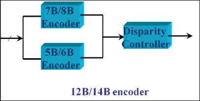
Fig. 3. 12B/14B Encoder Block Diagram
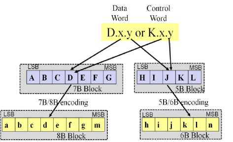
Fig. 4. Nomenclature for 12B/14B Encoding Technique
-
A. Disparity Control
Disparity is bounded between ±4, at sub-block level, block level, packet level, and even in whole stream. So, 8B block can have maximum 6 ones and minimum 2 ones. Disparity is higher for 7B/8B because 2 7 = 128 encoded data are required. For 8B codes, 70 ( 8 C 4 ) DC balanced codes and 56 ( 8 C 5 ) code of disparity ±2. For remaining 2 codes, ±4 disparity codes 56 ( 8 C 6 = 28) need to be considered. While, in 8B/10B encoding, disparity is bounded between ±2.
For controlling the disparity, disparity of current block and previous running disparity is checked. If combination of these two goes beyond limit, then current encoded block (8B or 6B) is complemented, this inverts current block disparity. This is shown in following table.
Table 3. Disparity Control Approach
|
Previous running disparity |
Current block disparity |
C omplement decision |
After block tx running disparity |
|
+4 (StateJJ) |
4 |
complement |
0 |
|
2 |
complement |
2 |
|
|
0 |
- |
4 |
|
|
-2 |
- |
2 |
|
|
-4 |
- |
0 |
|
|
+2(State_l) |
4 |
complement |
-2 |
|
2 |
complement |
0 |
|
|
0 |
- |
2 |
|
|
-2 |
- |
0 |
|
|
-4 |
- |
-2 |
|
|
0 (State_2) |
4 |
- |
4 |
|
2 |
- |
2 |
|
|
0 |
- |
0 |
|
|
-2 |
- |
-2 |
|
|
-4 |
Complement |
4 |
|
|
-2(State_3) |
4 |
- |
2 |
|
2 |
- |
0 |
|
|
0 |
- |
-2 |
|
|
-2 |
complement |
0 |
|
|
-4 |
complement |
2 |
B. Maximum Run Length control
Encoding technique is designed such that, maximum run length is limited to 7 only, at sub-block level, block level, packet level, and even in whole stream.
So if previous 6B is 000111, then next 8B can’t be 11111000, even when disparity allows this situation. These special cases are considered separately. To achieve this, at trailing and starting maximum 4 contiguous identical symbols are allowed in 7B/8B encoding and maximum 3 contiguous identical symbols are allowed in 5B/6B. If such codes come, then complementation is done to limit run length.
-
C. Encoding Map
Block diagram of encoder is shown in Fig. 5. Invalid control characters were also detected. Running disparity is kept within +4, ±2, 0. Disparity ‘-4’ is not used as it is not required. Disparity control block decides whether output code will be complemented or not. Based on previous disparity and current encoded output, an output disparity (i.e. running disparity) is generated, which will be used while encoding for next block. Table 4 shows 7B/8B encoding map for few 7B codes.
-
• For DC balance cases, output disparity is same as input disparity.
-
• For cases of disparity +2/+4, input disparity should be negative, otherwise complemented 8B (alternate) is transmitted.
-
• Encoding for control characters is different.
-
• Encoding for special cases (which can violate maximum run length rule) is also different (case D.15).
Fig. 5. 12B/14B Encoder block diagram
Disparity ‘++’ means +4, ‘+’ means +2 and ‘-’ means -2.
Table-5 shows 5B/6B encoding map. D.x.15 is coded differently, as it may violate maximum run length rule.
Table 6 shows encoding table for control characters. 12B/14B provides 4 COMMA characters (K.120.3, K.120.11, K.120.15 and K.120.19) and 18 other control characters too. These control characters can be assigned to IDLE, start of packet, end of packet, word alignment, abort and idle.
COMMA characters are singular in nature i.e. they must not appear in other sequence of valid bits including overlapped data characters. Also, they must occur with a uniform alignment relative to byte boundaries. To insert these properties in codes, Run length of 7 is kept only for COMMA characters. Encoding is done such that even a single bit error cannot change a valid code to COMMA character. For all control characters, complement form is required. Control characters are encoded differently.
Table 4. 7B/8B Encoding Map
|
Name |
Input 7В |
Disparity |
Output 8B abcde fg m |
Disparity |
alternate 8B abcde fg m |
Name |
Input 5B |
Disparity |
Output 6B |
Disparity |
alternate 8B |
||
|
ABCUt |
rw |
HIJK L |
Din |
hijk I n |
Dout |
hijk I n |
|||||||
|
D.O |
00000 |
00 |
01011 00 0 |
10100 11 1 |
D/K.x.O |
0000 0 |
+ |
0110 0 0 |
- |
1001 1 1 |
|||
|
D.1 |
10000 |
00 |
10001 11 1 |
+ |
01110 00 0 |
D/K.x.1 |
1000 0 |
+ |
1000 1 0 |
- |
0111 0 1 |
||
|
D.2 |
01000 |
00 |
- |
01110 10 1 |
10001 01 0 |
D/K.x.2 |
0100 0 |
+ |
0100 1 0 |
- |
1011 0 1 |
||
|
D.3 |
11000 |
00 |
11000 10 0 |
00111 01 1 |
D.x.3 |
1100 0 |
X |
1100 0 1 |
0 |
||||
|
0.12 |
00110 |
00 |
+ |
00110 10 0 |
11001 01 1 |
D/K.x.4 |
0010 0 |
+ |
0010 1 0 |
- |
1101 0 1 |
||
|
D.13 |
10110 |
00 |
X |
10110 00 1 |
0 |
D.x.5 |
1010 0 |
X |
1010 0 1 |
0 |
|||
|
D.15 |
11110 |
00 |
- |
11110000 |
0 |
00001 11 1 |
D.x.6 |
0110 0 |
X |
0110 0 1 |
0 |
||
|
D.22 |
01101 |
00 |
X |
01101 00 1 |
0 |
D/K.x.7 |
1110 0 |
- |
1110 0 0 |
0 |
0001 1 1 |
||
|
D.29 |
10111 |
00 |
X |
10111 00 0 |
0 |
D/K.x.8 |
0001 0 |
+ |
0001 1 0 |
- |
1110 0 1 |
||
|
D.30 |
01111 |
00 |
X |
01111 00 0 |
0 |
D.x.9 |
1001 0 |
X |
1001 0 1 |
0 |
|||
|
D.31 |
11111 |
00 |
+ |
10011 00 0 |
01100 11 1 |
D.x.10 |
0101 0 |
X |
0101 0 1 |
0 |
|||
|
D.39 |
11100 |
10 |
X |
11100 100 |
0 |
D.x.11 |
1101 0 |
X |
1101 0 0 |
0 |
|||
|
D.40 |
00010 |
10 |
00011 01 0 |
11100 10 1 |
D.x.12 |
0011 0 |
X |
0011 0 1 |
0 |
||||
|
D 49 |
10001 |
10 |
X |
10001 10 1 |
0 |
D.x.13 |
1011 0 |
1011 0 0 |
|||||
|
X |
0 |
||||||||||||
|
D.50 |
01001 |
10 |
X |
01001 10 1 |
0 |
||||||||
|
0.51 |
11001 |
10 |
X |
11001 10 0 |
0 |
D.x.14 |
0111 0 |
X |
0111 0 0 |
0 |
|||
|
D.52 |
00101 |
10 |
X |
00101 10 1 |
0 |
D.x.15 |
1111 0 |
- |
1111 00 |
0000 1 1 |
|||
|
0.53 |
10101 |
10 |
X |
10101 100 |
0 |
D/K.X.A15 |
1111 0 |
- |
0011 1 1 |
1100 0 0 |
|||
|
K.55.15 |
11101 |
10 |
— |
11101 10 1 |
++ |
00010 01 0 |
D/K.x.16 |
0000 1 |
- |
0110 1 1 |
+ |
1001 0 0 |
|
|
0.56 |
00011 10 |
X |
00011 10 1 |
0 |
D.x.17 |
1000 1 |
X |
1000 1 1 |
0 |
||||
|
0.57 |
10011 |
10 |
X |
10011 100 |
0 |
D.x.18 |
0100 1 |
X |
0100 1 1 |
0 |
|||
|
K.57.15 |
10011 |
10 |
10011 10 1 |
+ |
01100 01 0 |
D.x.19 |
1100 1 |
X |
1100 1 0 |
0 |
|||
|
D.58 |
01011 |
10 |
X |
01011 10 0 |
0 |
D.x.20 |
0010 1 |
X |
0010 1 1 |
0 |
|||
|
0.59 |
11011 |
10 |
- |
11011 100 |
+ |
00100 01 1 |
D.x.21 |
1010 1 |
X |
1010 1 0 |
0 |
||
|
0.64 |
00000 |
01 |
++ |
00100 01 0 |
11011 10 1 |
D.x.22 |
0110 1 |
X |
0110 1 0 |
0 |
|||
|
0.85 |
10101 |
01 |
X |
10101 01 0 |
0 |
D/K.X.23 |
1110 1 |
- |
1110 1 0 |
0001 0 1 |
|||
|
0.86 |
01101 |
01 |
X |
01101 01 0 |
0 |
D/K.x.24 |
0001 1 |
0011 0 0 |
- |
1100 1 1 |
|||
|
0.87 |
11101 |
01 |
- |
11101 01 0 |
+ |
00010 10 1 |
D.x.25 |
1001 1 |
X |
1001 1 0 |
0 |
||
|
K.87.15 |
11101 |
01 |
-- |
11101 01 1 |
++ |
00010 10 0 |
D.x.26 |
0101 1 |
X |
0101 1 0 |
0 |
||
|
0.88 |
00011 |
01 |
X |
00011 01 1 |
0 |
D/K.x.27 |
1101 1 |
1101 1 0 |
0010 0 1 |
||||
|
0.92 |
00111 |
01 |
X |
00111 01 0 |
0 |
||||||||
|
01000 10 1 |
D.x.28 |
0011 1 |
X |
0011 1 0 |
0 |
||||||||
|
0.93 |
10111 |
01 |
— |
10111 01 0 |
|||||||||
|
k.93.15 |
10111 |
01 |
10111 01 1 |
++ |
01000 10 0 |
D/K.x.29 |
1011 1 |
- |
1011 1 0 |
0100 0 1 |
|||
|
D.126 |
01111 |
11 |
00101 11 1 |
4- |
11010000 |
D/K.x.30 |
0111 1 |
- |
0111 1 0 |
1000 0 1 |
|||
|
0.127 |
11111 |
11 |
10010 11 1 |
* |
01101 00 0 |
D/K.x.31 |
1111 1 |
- |
1010 1 1 |
0101 0 0 |
|||
Table 5. 5B/6B Encoding Map
Table 6. Encoding Map for Control Characters
7В input 5В input Disparity 8B output 6B output Disparity alternate output
|
NAME |
ABCDE FG |
HIJK L |
Din |
abcde fg m |
hijkln |
Dout |
abcde fg m |
hijkln |
|
K.120.0 |
' 0001111 |
0000 0 |
- |
00011111 ' |
011000 |
0 |
11100000 |
100111 |
|
K.120.1 |
0001111 |
1000 0 |
- |
00011111 |
100010 |
0 |
11100000 |
011101 |
|
K.120.2 |
r 0001111 |
0100 0 |
- |
' 00011111 r |
010010 |
0 |
11100000 |
101101 |
|
K.120.3 |
r 0001111 |
1100 0 |
- |
' 00011111 |
110001 |
+ |
11100000 |
' 001110 |
|
K.120.4 |
' 0001111 |
0010 0 |
- |
' 00011111 ’ |
001010 |
0 |
11100000 |
' 110101 |
|
K.120.7 |
0001111 |
1110 0 |
- |
00011111 r |
000111 |
+ |
11100000 |
111000 |
|
K.120.8 |
" 0001111 |
0001 0 |
- |
' 00011111 r |
000110 |
0 |
11100000 |
' 111001 |
|
K.120.11 |
r 0001111 |
1101 0 |
- |
' 00011111 r |
110100 |
+ |
11100000 |
' 001011 |
|
K.120.15 |
r 0001111 |
11110 |
- |
' 00011111 r |
110000 |
0 |
11100000 |
' 001111 |
|
K.120.16 |
r 0001111 |
0000 1 |
- |
' 00011111 r |
100100 |
0 |
11100000 |
' 011011 |
|
K.120.19 |
' 0001111 |
1100 1 |
- |
00011111 ' |
110010 |
+ |
11100000 |
001101 |
|
K.120.23 |
' 0001111 |
1110 1 |
- |
00011111 r |
000101 |
0 |
11100000 |
' 111010 |
|
K.120.24 |
0001111 |
0001 1 |
- |
00011111 |
001100 |
0 |
11100000 |
110011 |
|
K.120.27 |
r 0001111 |
1101 1 |
- |
' 00011111 r |
001001 |
0 |
11100000 |
' 110110 |
|
K.120.29 |
r 0001111 |
1011 1 |
- |
' 00011111 r |
010001 |
0 |
11100000 |
' 101110 |
|
K.120.30 |
' 0001111 |
0111 1 |
- |
' 00011111 ’ |
100001 |
0 |
11100000 |
' 011110 |
|
K.120.31 |
" 0001111 |
1111 1 |
- |
00011111 r |
010100 |
0 |
11100000 |
' 101011 |
|
K.55.15 |
1110110 |
11110 |
- |
11101101 |
110000 |
’ 00010010 |
■ 001111 |
|
|
K.57.15 |
1001110 |
1111 0 |
- |
10011101 |
110000 |
0 |
' 01100010 |
001111 |
|
K.87.15 |
1110101 |
1111 0 |
- |
11101011 |
110000 |
+ |
00010100 |
001111 |
|
K.93.15 |
1011101 |
11110 |
- |
' 10111011 |
110000 |
+ |
” 01000100 |
' 001111 |
K.117.15 1010111 11110 - 10101111 110000 + 01010000 001111
-
D. Decoding Map
Block diagram of implemented decoder is shown in Fig 6. Invalid codes are detected first. Disparity check is also performed to detect any error. These are explained in next section.
Decoding map for 8B/7B and 6B/5B is shown in Table 7 and 8 respectively. For any code, decoded code is unique, it doesn’t depend on disparity. So, even if some code shows disparity violation, remaining code will be decoded without any error.
Fig. 6. Decoder Block Diagram
Table 7. 8B/7B Decoding Map
|
Name |
Input 8 В |
Output 7B |
к |
Disparity |
Disparity |
|
|
abcde fq m |
ABCDE |
FC |
Din |
Пт it |
||
|
DO |
01011 000 |
00000 |
00 |
0 |
+ |
|
|
DO |
10100 11 1 |
00000 |
00 |
0 |
- |
+ |
|
D.1 |
10001 11 1 |
10000 |
00 |
+ |
||
|
D.1 |
01110 00 0 |
10000 |
00 |
+ |
- |
|
|
D.25 |
10101 00 1 |
10101 |
00 |
о |
X |
o |
|
D.26 |
01101 00 1 |
01101 |
00 |
n |
X |
о |
|
D.27 |
11101 000 |
11101 |
00 |
X |
о |
|
|
D.55 |
00010 01 1 |
11101 |
10 |
о |
+ |
|
|
K.55.15 |
11101 10 1 |
11101 |
10 |
1 |
++ |
|
|
K.55.15 |
00010 01 0 |
11101 10 |
1 |
++ |
— |
|
|
D.56 |
00011 10 1 |
00011 |
10 |
0 |
X |
0 |
|
D.57 |
10011 100 |
10011 10 |
0 |
X |
0 |
|
|
K.57.15 |
10011 10 1 |
10011 |
10 |
1 |
+ |
|
|
K.57.15 |
01100 01 0 |
10011 10 |
1 |
+ |
||
|
D.58 |
01011 100 |
01011 |
10 |
0 |
X |
|
|
D.37 |
11101 01 0 |
11101 |
01 |
0 |
+ |
|
|
0.87 |
00010 10 1 |
11101 |
01 |
0 |
+ |
|
|
K.87.15 |
11101 01 1 |
11101 |
01 |
1 |
++ |
|
|
K.87.15 |
00010 10 0 |
11101 |
01 |
1 |
++ |
— |
|
D 88 |
00011 01 1 |
00011 |
01 |
0 |
X |
о |
|
D.89 |
10011 01 0 |
10011 |
01 |
Ci |
X |
|
|
D.97 |
10000 11 1 |
10000 |
11 |
X |
о |
|
|
D S8 |
01000 11 1 |
01000 |
11 |
Q |
X |
о |
|
D.99 |
11000 11 0 |
11000 |
11 |
X |
о |
|
|
D.109 |
10110 11 0 |
10110 |
11 |
о |
- |
+ |
|
D.109 |
01001 00 1 |
10110 |
11 |
0 |
+ |
|
|
D.110 |
01110 11 0 |
01110 |
11 |
0 |
+ |
|
|
D.116 |
00101 11 0 |
00101 |
11 |
0 |
X |
|
|
D.117 |
10101 11 0 |
10101 |
11 |
0 |
+ |
|
|
□.117 |
01010 00 1 |
10101 |
11 |
0 |
+ |
|
|
K.117.15 |
10101 11 1 |
10101 11 |
1 |
++ |
||
|
K.117.15 |
01010 00 0 |
10101 |
11 |
1 |
++ |
— |
|
D.118 |
01101 11 0 |
01101 |
11 |
0 |
+ |
|
|
D.118 |
10010 00 1 |
01101 |
11 |
0 |
||
|
D.118 |
11101 11 0 |
11101 |
11 |
0 |
++ |
|
|
D.119 |
00010 00 1 |
11101 |
11 |
0 |
++ |
— |
|
D.120 |
00011 11 0 |
00011 |
11 |
0 |
X |
о |
|
K.120.y |
00011 11 1 |
00011 |
11 |
- |
+ |
|
|
K.120.y |
11100 000 |
00011 |
11 |
1 |
+ |
|
|
D.121 |
10011 11 0 |
10011 |
11 |
Q |
- |
+ |
|
D.126 |
11010 000 |
01111 |
11 |
о |
+ |
|
|
D.127 |
10010 11 1 |
11111 |
11 |
n |
- |
+ |
D.127 01101 000 11111 11 0
Table 8. 6B/5B Decoding Map
|
Name |
Input 6B hijk I n |
Output SB HIJK L |
К |
Disparity |
Disparity |
|
Din |
Dout |
||||
|
D/K.X.O |
011000 |
0000 0 |
X |
+ |
|
|
D/K.X.O |
1001 1 1 |
0000 0 |
X |
+ |
|
|
D/K.x.1 |
100010 |
1000 0 |
X |
+ |
|
|
D/K.x.1 |
0111 0 1 |
1000 0 |
X |
+ |
|
|
D/K.x.2 |
010010 |
0100 0 |
X |
+ |
|
|
D/K.x.2 |
1011 0 1 |
0100 0 |
X |
||
|
D x.3 |
11000 1 |
11000 |
0 |
X |
0 |
|
K.120.3 |
11000 1 |
11000 |
1 |
+ |
0 |
|
К 120.3 |
0011 1 0 |
11000 |
1 |
0 |
|
|
D/K.x.4 |
001010 |
0010 0 |
X |
+ |
|
|
D/K.x.4 |
1101 0 1 |
0010 0 |
X |
+ |
|
|
D.x.S |
10100 1 |
10100 |
0 |
X |
0 |
|
D.x.6 |
0110 0 1 |
01100 |
0 |
X |
0 |
|
D/K.x.7 |
111000 |
11100 |
X |
0 |
|
|
D/K.x.7 |
0001 1 1 |
11100 |
X |
+ |
0 |
|
D/K.x.8 |
0001 1 0 |
0001 0 |
X |
+ |
|
|
D/K.x.8 |
11100 1 |
0001 0 |
X |
+ |
|
|
Dx.9 |
1001 0 1 |
1001 0 |
0 |
X |
0 |
|
D.x.10 |
0101 0 1 |
0101 0 |
0 |
X |
0 |
|
D.x.11 |
1101 00 |
1101 0 |
0 |
X |
0 |
|
K.120.11 |
1101 00 |
1101 0 |
1 |
+ |
0 |
|
К 120.11 |
0010 1 1 |
1101 0 |
1 |
0 |
|
|
D.x.13 |
1011 00 |
1011 0 |
0 |
X |
0 |
|
D.x.14 |
0111 0 0 |
0111 0 |
0 |
X |
0 |
|
D.X.P15 |
1111 00 |
1111 0 |
0 |
||
|
D.X.P15 |
0000 1 1 |
1111 0 |
0 |
||
|
D/K.X.A15 |
0011 1 1 |
1111 0 |
X |
* |
|
|
D/K.X.A15 |
110000 |
1111 0 |
X |
||
|
D/K.x.16 |
01101 1 |
0000 1 |
X |
4. |
|
|
D/K.x.16 |
1001 0 0 |
0000 1 |
X |
+ |
|
|
D.x.17 |
1000 1 1 |
1000 1 |
0 |
X |
0 |
|
D.x.15 |
01001 1 |
0100 1 |
0 |
X |
0 |
|
D.x.19 |
1100 1 0 |
1100 1 |
0 |
X |
0 |
|
К 120.19 |
1100 1 0 |
1100 1 |
1 |
+ |
0 |
|
K.120.19 |
0011 0 1 |
1100 1 |
1 |
0 |
|
|
D.x.20 |
0010 1 1 |
0010 1 |
0 |
X |
0 |
|
D.x.21 |
101010 |
1010 1 |
0 |
X |
0 |
|
D.x.22 |
0110 1 0 |
0110 1 |
0 |
X |
0 |
|
D/K.x.23 |
1110 10 |
1110 1 |
X |
4- |
|
|
D/K.x.23 |
0001 0 1 |
1110 1 |
X |
+ |
|
|
D/K.X.24 |
0011 0 0 |
0001 1 |
X |
+ |
|
|
D/K.x.24 |
11001 1 |
0001 1 |
X |
4- |
|
|
D.X.25 |
1001 10 |
1001 1 |
0 |
X |
0 |
|
D.x.26 |
0101 1 0 |
0101 1 |
0 |
X |
0 |
|
D/K.x.27 |
110110 |
1101 1 |
X |
4- |
|
|
D/K.x.27 |
0010 0 1 |
1101 1 |
X |
+ |
|
|
D.x.28 |
0011 1 0 |
0011 1 |
0 |
X |
0 |
|
D/K.x.29 |
1011 1 0 |
1011 1 |
X |
4. |
|
|
D/K.X.29 |
0100 0 1 |
1011 1 |
X |
+ |
|
|
D/K.x.30 |
0111 1 0 |
0111 1 |
X |
+ |
|
|
D/K.X.30 |
1000 0 1 |
0111 1 |
X |
+ |
|
|
D/K.x.31 |
1010 1 1 |
11111 |
X |
+ |
|
|
D/K.x.31 |
0101 00 |
11111 |
X |
-
E. Error Detection Capability
Error detection can be carried out by checking current decoded block disparity and previous block disparity (overall disparity should be within ±4).
Single and multiple bit error can be checked by detecting invalid combinations. Out of 16384 codes, only 7012 codes (57%) are valid codes. This can be explained as follows.
-
• Codes that doesn’t require complementation (like 01011010 i.e. both DC balanced and no maximum run length violation) for 8B =68 codes, for 6B = 18 codes, overall 68 * 18 = 1224 codes.
-
• Remaining 4096-1224 = 2872 codes requires two output forms.
-
• Control characters = 22 (all control char have alternate form).
So, overall valid decoded data = (2872 * 2) + 1224 + (22*2) = 7012.
-
IV. Implementation Results
Data flow can be summarized as follows. After every power-on sequence, this sequence should be followed.
-
1. Idle packet transmission for receiver initialization and locking
-
2. Word alignment sequence transmission
-
3. Idle sequence transmission (optional)
-
4. Start of packet transmission
-
5. Data packet transmission
-
6. End of packet transmission (optional)
-
7. Idle sequence transmission (optional)
Implementation (Encoder-Decoder):
However LUT based implementation was possible, combinational logic based design was carried out to save logic area for other functional blocks.
The encoder and decoder designs are simulated for space grade FPGA. The simulated report summary is given in Table 8.
Table 8. Simulation Results Summary
|
Parameter |
Encoder |
Decoder |
|
Total Logic |
205 / 32248 |
235 / 32248 |
|
Elements |
(<1%) |
(<1%) |
|
Requested Sampling rate |
100 MHz |
100 MHz |
|
Achieved Sampling rate |
63 MHz |
58 MHz |
The implemented SERDES Encoder/Decoder meets all specifications. It meets the sampling rate requirement of future mission (>40MSPS). As a next step, design of other functional blocks like timing-logic, PLL, LVDS drivers and CDR has been initiated.
-
V. Conclusion
A technology-independent design is carried out in FPGA. Planned interface will reduce interfaces by a factor of 12. Differential serial transmission will result in power reduction by factor of 12. Weight/volume reduction would be quite signification as less number of connectors/harnesses/packages will be required. The design occupies only a small portion of the available logic resources, indicating that it can be integrated with other functional blocks of the sub-systems. Same design can work for higher speed with selection of higher speed FPGA. This design can be integrated with other block of SERDES. Timing logic design can be having higher redundancy in case of bit errors.
Список литературы Design of 12B/14B: A Novel SERDES Encoding Technique
- Datasheet of COTS SERDES (TLK2711, DS90UR241)Dave Lewis, “SERDES Architecture and Applications”, application note by National Semiconductor Corporation
- Ashok Kumar, Sanjeev Mehta, “Indigenous Development of SERDES Interface for Miniaturization”, 1st International conference on emerging technology trends in electronics, communication and networking, pp 1-6 (2012)
- X. Widmer and P. A. Franaszek, “A DC-Balanced, Partitioned -Block, 8Bl10B Transmission Code”, IBM J Res. Develop. 27, 440-451 (1983).
- Actel, “Implementing an 8B/10B Encoder/Decoder for Gigabit Ethernet in the Actel SX Family”, Application Note.
- XILINX, XAPP336 (v1.3), “Design of a 16b/20b Encoder/Decoder Using a CoolRunner XPLA3 CPLD”
- Lattice semiconductor Corporation,“8B/10B Encoder/Decoder”, Reference Design RD1012
- “Data Encoding Techniques”, www.rhyshaden.com
- Ashok Kumar, “Electrical evaluation of Very High Speed Data Transmission Device”, National Conference on Advances in Engineering and Science, April 2012.
