Filter Loop Reduction in DT BP Sigma-Delta Modulator Assisted by Noise Coupling Technique

Author: Reza Gholami, Gholamreza Ardeshir, Hossein Miar-Naimi
Journal: International Journal of Intelligent Systems and Applications(IJISA) @ijisa
Article in issue: 8 vol.6, 2014.
Free access
In bandpass modulators, a 2N-order loop filter can lead to an N-order noise shaping in the band of interest. This caused a bandpass modulator with more complex structure than a lowpass modulator and increased the power consumption and area of the modulator. In this paper, we proposed a discrete-time bandpass modulator using the noise-coupling technique that only needs to a second- order loop filter to have a second-order noise shaping. To realize a noise coupled bandpass modulator, we need to implement Z-2 delay block in the analog domain, but the proposed modulator uses only Z-1 delay blocks to apply the noise coupling technique. This simplifies the structure of the modulator and reduces the power consumption, area, and nonlinearity of the modulator. The error in the coupling path is considered and the effect of it on the modulator resolution is analyzed. According to the simulation results, the proposed modulator results in SNR = 84.9 dB at 80 MHz sampling frequency, 200 KHz bandwidth and OSR = 200.
Sigma-delta modulator, bandpass, discrete-time, noise coupling, loop filter
Short address: https://sciup.org/15010587
IDR: 15010587
Text of the scientific article Filter Loop Reduction in DT BP Sigma-Delta Modulator Assisted by Noise Coupling Technique
Published Online July 2014 in MECS DOI: 10.5815/ijisa.2014.08.01
Considering the development of different wireless standards in RF communication systems, trends have evolved towards multi-standard receivers that are compatible with different modulations, bandwidths, and SNRs. One way to realize this receiver is to perform the analog to digital conversion closer to antenna [1]-[3]. Regarding this, to implement multi-standard receivers, wideband and high resolution converters are needed. Also, these converters should have low power consumptions in order to increase the battery life.
Bandpass sigma-delta modulators are suitable for such systems because analog to digital conversion occurs only in the desired band around the central frequency (Fc) of the modulators. Thus, they have high resolution, low power consumption, and little sensitivity to low frequency noise and offset comparing to lowpass modulator [2].
To achieve an N-order noise shaping in the bandpass modulators, a 2N-order loop filter is needed. This results in higher power consumption, more area, and circuit complexity. On the other hand, there are three design factors to increase the resolution of the sigma-delta modulator [4], [5]: (1) the number of quantizer bits; (2) order of loop filter; (3) oversampling ratio (OSR).
Increasing each one of these factors results in higher resolution at the cost of more power consumption.
To reduce the circuit complexity and power consumption, different solutions have been proposed. A power-efficient resonator has been proposed based on positive feedback. It used only one opamp that halves the power consumption of the modulator [6]. In [7] a hybrid loop filter is used in the modulator to reduce the power consumption. Also in [8] a new resonator is proposed to reduce the circuit complexity of the modulator. In the aforementioned architectures, changing the resonator at system or circuit level is the way that used to reduce power consumption and circuit complexity. Doublesampling technique was used in [9] which reduces the number of opamps to one for each resonator. This caused reduction of the resonator power consumption. Also, this technique doubles the settling time of the resonators and simplifies the design of the opamps [10].
Another way is to use the noise coupling technique. This technique is used to increase the order of the lowpass [11]-[18] and complex bandpass modulators [19], [20]. In this technique, processing of the quantization noise and applying it to the quantizer input can lead to increase order of the noise shaping. If the order of the noise shaping in noise coupled modulator is identical to that of the conventional modulator, then the noise coupled modulator has been lower order loop filter comparing to conventional one. Reduction of the loop filter order results in lower power consumption and less complex circuitry. Furthermore, this technique reduces the nonlinearity and improves dynamic range of the modulator.
In this paper, we used noise coupling technique to reduce the order of the loop filter in bandpass modulators. We need to implement Z-2 delay block to be able to use this technique in bandpass modulators. Implementation of Z-2 delay block is a difficult task in the analog circuits design because it needs complicated clock signals [14]. To tackle this problem, the proposed modulator is designed such that it only needs Z-1 delay blocks. This paper is organized as follows. Using noise coupling technique in the lowpass modulators is described in Section II. In Section III, the proposed modulator is studied and Section IV compares the simulation results of the proposed modulator with the conventional one. Finally, the conclusion is given in section V.
II. Noise Coupling Technique in Lowpass
Modulators
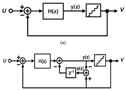
Noise coupling technique has been used to increase the order of the lowpass sigma-delta modulators. Figure 1(a) shows a conventional lowpass modulator.
(b)
Fig. 1. (a) Conventional lowpass modulator; (b) First order noise coupled modulator
According to (7), one zero at DC frequency is added to the noise transfer function of the modulator. It is caused the order of the noise shaping increases by one. Therefore, by choosing an integrator as the loop filter, the NTF of the noise coupled modulator will be of order 2. Noise coupled modulator is achieved the 2-order noise shaping while it only uses one integrator inside the loop. By choosing a suitable noise coupling function, higher order noise shaping can be achieved. For example, by choosing 2Z-1-Z-2 as the noise coupling function, 3-order noise shaping can be achieved.
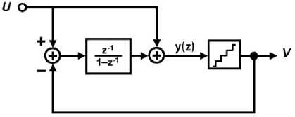
A first order low distortion modulator and a second order one are shown in Figure 2(a) and Figure 2(b), respectively [21]. By applying the input signal directly to the input node of the quantizer, the loop filter only processes the quantization noise. This reduces the amplitude of the internal signals and the nonlinear effects in the modulator and therefore simplifies the design of the opamps. Also, a first order noise coupled modulator is shown in Figure 2(c).
Using linear approximation for the qunatizer, the noise transfer function (NTF) and signal transfer function (STF) of the modulator are obtained as follows:
v ( z ) = [ ( u ( z ) - v ( z ) )x H ( z ) ] + E ( z ) (1)
v ( z) = u (z) x 1 + Hzz ) + £ ( z) x i + Hz ) (2)
(a)
STF =
H ( z )
1 + H ( z )
NTF
1 + H ( z )
In (1), v(z) is the modulator output, u(z) is the modulator input, ε(z) is the quantization noise and H(z) is the transfer function of the loop filter. If an integrator is used as the loop filter, STF will be a delay function and NTF will be a highpass function.
A first order noise coupled modulator is shown in Figure 1(b) [13]. Quantization noise E(z) is obtained by subtracting the modulator output from the quantizer input and is fed back to the input node of the quantizer after one clock period according to Figure 1(b). This increases the order of the modulator without any change at the loop filter architecture. To apply the noise coupling technique, we need one adder and one Z-1 delay block as shown in Figure 1(b). The z-domain equations for the noise coupled modulator can be expressed as follows:
e(z) = v(z) - y(z) = e( z)
v(z) = [(u(z)-v(z))xH(z)] - z 1 x ^(z) + ^(z)
v(z) = u (z)x 1+H(z) + f(z) x(1 z )x 1+H(z)
NTF = з x x (1-z-1) = NTF x (1-z-1)(7)
new 1+H (z)
(b)
(c)
Fig. 2. (a) First order low distortion modulator; (b) Second order low distortion modulator; (c) First order noise coupled modulator
Both the second order low distortion modulator and noise coupled modulator are achieved 2-order noise shaping while the noise coupled modulator needs only one integrator inside the loop. This shows that using noise coupling technique can reduce the order of the loop filter in the modulator. In the noise coupled modulator, in comparison with the modulator of Figure 2(b), an Integrator has been removed and a delay block has been added instead.
Using noise coupling technique improves the linearity and stability of the modulator. This occurs because there
are several factors that cause the coupled noise acts as a dither input [12]. These factors are: thermal noise, Flicker noise, offset, mismatch errors, and the nonlinearities of the opamps and switches.
The noise coupled modulator is designed as the low distortion architecture, thus it does not need another adder to couple the noise to the modulator. Regarding this, the number of active elements in the noise coupled modulator is decreased and therefore the power consumption and circuit complexity is reduced.
Also, design of the noise coupled modulator as the low distortion architecture improves the linearity of the modulator because the amplitude of the internal signal is reduced in this architecture. According to Figure 2(c), the NTF and STF of the modulator can be expressed as follows:
e ( z ) = v ( z )- y ( z ) = e ( z )
v ( z) = ( u ( z ) - v ( z ) ):
z
. -1
1 - z -
-
z
- 1
x e(z) + u (z) + e(z)
v (z) = u (z) x 1 + e( z) x (1-z 1)
STF = 1, NTF = (1-z-1)2
-
III. Proposed Modulator
Bandpass modulators are used to digitize the IF and RF signals. If an IF or RF signal is wanted to digitize, using these modulators have several important advantages compared with the lowpass modulators, including little sensitivity to the offset and low frequency noise, higher resolution, and greater reliability. The power consumption of these modulators is less than lowpass modulators because the analog to digital conversion performs only in the band of interest around the central frequency (F c ) of the modulators. To digitize an IF or RF signal by a lowpass modulator, a very high bandwith is needed. It is caused the lowpass modulators have more power consumption than the bandpass one.
To convert the RF and IF signals, we need a bandpass modulator that has a loop filter with complex conjugate poles. Thus, to achieve an N-order noise shaping, a 2N-order loop filter is needed. One way to realize a bandpass modulator is using the conventional mathematical transformation to transform a lowpass architecture to a bandpass one [23]. This transformation is
Z - 1 ^- Z - 2 (12)
By applying (12) to a lowpass modulator, the zeros of NTF move to a non-zero frequency on the unity circle. In system level, this is equivalent to replace the integrators by resonators in the lowpass modulator. This lead to a bandpass modulator that has complex conjugate poles on the unity circle at Fs/4 frequency. Using the resonators instead of integrators in bandpass modulators causes the NTF of the bandpass modulator to be a band-stop transfer function. Regarding this, the modulator shapes the quantization noise away from the frequencies around Fs/4.
A conventional fourth order bandpass modulator is shown in Figure 3 that it has a second order noise shaping in the Fs/4 Frequency [22]. The A and B coefficients are used to adjust the internal signal swings of the modulator.
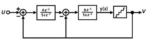
Fig. 3. Conventional 4-order bandpass modulator
By applying the transformation of (12) to the first order noise coupled modulator that is shown in Figure 2(c), a noise coupled bandpass modulator is realized. In system level, this is equivalent to replace the integrator by a resonator and Z-1 delay block by a Z-2 delay block. Figure 4 is shown the noise coupled bandpass modulator.
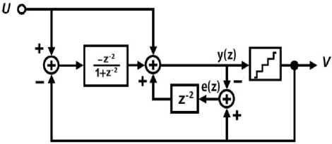
Fig. 4. Noise coupled bandpass modulator
In this architecture, quantization noise is applied to the quantizer input after two clock periods. This increases the order of the noise shaping by one. According to Figure 4, the z-domain equations for the modulator are obtained as follows:
e ( z ) = v ( z )- У ( z ) = e ( z )
v ( z ) = ( u ( z ) - v ( z ) ) x
- z - 2 1 + z - 2
- 2
+ z x e ( z ) + u ( z ) + e ( z )
v ( z ) = u ( z ) + e ( z ) x ( 1 + z 2 )
STF = 1 , NTF = ( 1 + z 2 ) 2
Equation (16) shows the order of the noise shaping in the modulator of Figure 4 is identical to the conventional fourth order modulator, while it uses only one resonator inside the loop. Thus, the order of the loop filter in the noise coupled modulator is reduced by the noise coupling technique. The modulator of Figure 4 makes use of low distortion architecture to reduce the internal swings and the nonlinear effects in the modulator. Using low distortion architecture is caused the STF of the modulator to be flat according to (16).
To realize the noise coupled bandpass modulator, we need to implement Z-2 delay block. Implementation of such delay block is a difficult task in the analog circuits design because it needs complicated clock signals. One way to solve this problem is to implement it as the time interleaved architecture [24].
Although, the time interleaved architecture simplifies the implementation of Z-2 delay block but the nonidealities and timing mismatches among paths make spurious tones in the band of interest. This reduces the resolution of the modulator. The time interleaved architecture reduces the power consumption by reducing the sampling frequency of each path, but increases the complexity and area of the modulator.
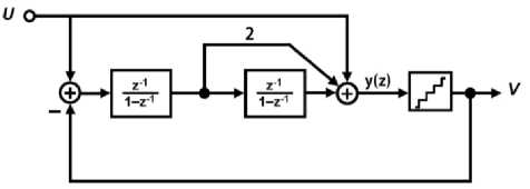
In this paper, a noise coupled bandpass modulator is proposed that need not to implement Z-2 delay block. The proposed modulator is shown in Figure 5 that only needs Z-1 delay blocks.
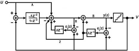
Fig. 5. Proposed second order bandpass modulator
The A and B coefficients in this modulator are used for dynamic range scaling. If A = B = 1 and the linear model for the quantizer is considered, NTF and STF of the modulator are obtained as follows:
e 1( z ) = v ( z )- y ( z ) = £ ( z )
-L
6 2 ( z ) = £ ( z ) x (1 + z )
v ( z ) = ( u ( z ) - v ( z ) ) x-
- 2
- z
1 + z - 2
+ z 1 x e 2( z )
- 2 z 1 x e i( z ) + u ( z ) + z 1 x e ^( z ) + £ ( z )
V ( z ) = U (z ) + £ (z ) x ( 1 + Z 2 )
STF = 1, NTF = ( 1 + z 2 ) 2
According to (21), STF = 1 and therefore input signal appears in the output without any change. The NTF of the proposed modulator has 4 complex conjugate zeros at Z=±j on the unity circle. Thus, this modulator has a noise shaping of order 2 in the F s /4 frequency while it uses only a second order filter inside the loop. Considering the NTF of the proposed modulator, quantization noise is attenuated in the desired band and it is increased near F s /2 and DC frequencies. By removing the out-of-band noise by decimation filter at the modulator output, resolution of the modulator is increased.
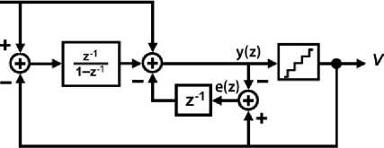
The equivalent block diagram of the proposed modulator is illustrated in Figure 6. According to Figure 6, only Z-1 delay block is used in the coupling paths that it can be easily implemented in the analog domain. If it is assumed that the conventional modulator of Figure 3 makes use of low distortion architecture, the derived modulator has two resonators and one adder. Therefore, a low distortion conventional modulator needs 5 opamps. Comparing this with the proposed modulator shows that one resonator is removed in the proposed modulator while two Z-1 delay blocks and one adder are added to it according to Figure 6.
Also Z-1 delay blocks in the feedback paths are easily implemented in the digital domain. Regarding this, the proposed modulator needs 4 opamps to be implemented, although it is designed as the low distortion architecture. Thus the proposed modulator consumes less power and has reduced number of the active elements.
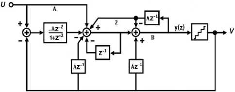
Fig. 6. Equivalent block diagram of proposed modulator
In this architecture two adders are needed to couple the noise to the modulator. It is caused more power consumption but the proposed modulator has advantage of zero optimization [2]. The zero optimization can be done by adjusting the gain of path with gain 2 while the modulator of Figure 4 does not have this ability. Choosing proper gain for this path is caused to increase the resolution of the modulator. Figure 7 shows the proposed modulator with zero optimization.
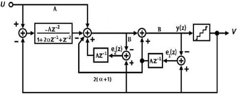
Fig. 7. Proposed modulator with zero optimization
Zero optimization technique moves the zeros of NTF to the optimum frequencies that are obtained as follows [9]:
F
Fs
0 4 ±
Fb 23
According to the resonator transfer function and couple path function, the value of α that is caused to place the zeros at optimum frequencies is given
a
[
= sin П x OSR 1 273
Noise coupling technique improves the linearity of the sigma-delta modulator because the correlation of the quantization noise and coupled noise is very low. In fact, coupled noise acts as a dither input. Adding a dither input to the modulator randomizes the signals and reduces the correlation of those. This diminishes the spurious tones at the output of the modulator. Temperature noise and nonideal effects in the opamps and coupling paths result in decorrelation of the quantization noises in the modulator [25].
Although, the noise coupling technique reduces the nonlinear effects in the modulator, but increases the swing of the internal signals. Increasing the number of quantizer bits can be reduced the amplitude of the quantization noise and therefore results in reduction of the signal swings at the internal nodes of the modulator. In the proposed modulator, dynamic range scaling is used to reduce the swing of the internal signals. By choosing suitable values for A and B, the signal swing can be adjusted to a reasonable range.
The noise coupling technique does not affect the stability of modulator because the noise coupling paths do not change the loop gain of the modulator. Thus the stability of the proposed modulator is comparable to that of a conventional 4-order modulator with dither.
If the quantization noise is coupled to the modulator input, the noise coupled architecture would have been very sensitive to the coupling path errors [2]. However, in the proposed modulator, noise is coupled to the quantizer input. It is caused the errors do not have significant effect on the resolution of the modulator because the loop filter has a high in-band gain and therefore it attenuates the added noise to the modulator output that is caused by theses errors.
As illustrated in Figure 8, if the coupling paths errors are considered, the noise transfer function of the modulator is obtained as follows:
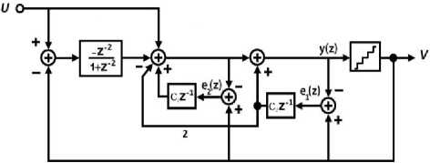
Fig. 8. Proposed modulator with gain error in coupling paths
IV. Simulation Results
Nonideal effects of the opamps and other elements that used in the sigma-delta modulator affect its real behavior. In this paper, the behavior of the modulator is simulated by taking into account all nonideal effects such as: KT/C noise, sampling jitter, and opamps nonideal parameters [26]. Simulation results of the proposed modulator are compared with the conventional modulator of Figure 3. In Table 1 the values used for nonideal effects in both modulators are shown.
Table 1. Nonideal Parameters’ Values
|
Parameter |
Value |
|
Sampling jitter |
6 ps |
|
Sampling Capacitor |
0.8 pf |
|
Opamp Finite Gain |
30 dB |
|
Opamp Finite Bandwidth |
100 MHz |
|
Opamp Slew Rate |
400 V/µs |
|
Saturation Voltage |
±1 V |
Only the nonideal effects of the first resonator are considered because the effect of nonidealities in the second resonator or coupling paths are shaped by the same transfer function as the quantization noise and do not have significant effect on the modulator output.
e1 ( z ) = v ( z) - y ( z) = e ( z) (24)
- 1
62 ( z ) = e ( z ) x (1 + C 2 Z ) (25)
NTF
(l + z ^) x ( l + C 1 C 2 z ^)-
I + ( C 1 - C 2) x z
.-1
The error of path with gain of 2 is disregarded to simplify the analysis. According to (26), errors in coupling paths move the NTF zeros. Thus, the zeros of NTF do not happen at F s /4 frequency and the noise in the desired band is increased. According to this equation, added noise is shaped by 1+ Z-2 function and therefore the paths error effect on the resolution is reduced.
By reducing the order of the loop filter and the number of active elements in the proposed modulator, the power consumption, area, and circuit complexity of the modulator are reduced while this reduction does not affect the first resonator architecture.
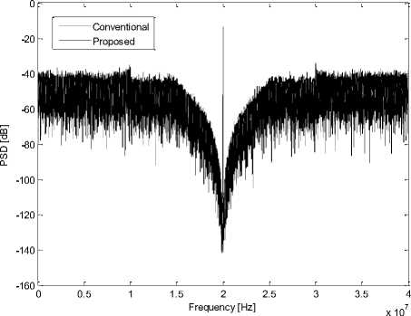
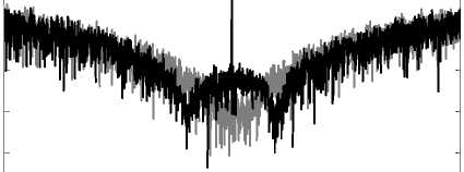
Fig. 9. Power spectral densities of the proposed modulator and the modulator of Figure 3
Values for A and B are chosen by simulation, such that the value of SNDR becomes Maximum. In both modulators, these coefficients are chosen A = 0.4 and B = 2.5 according to the exhaustive simulation results. The
power spectral densities of the proposed modulator and the conventional modulator of Figure 3 are shown in Figure 9.
According to Figure 9, the proposed modulator acts as a conventional fourth order modulator and achieves a second order noise shaping. The NTF of the proposed modulator is the same as a band-stop filter. According to (21), the central frequency of the proposed modulator is expected to be at F s /4 frequency that it is clear from Figure 9.
Input Amplitude [dB]
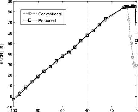
Fig. 10. SNDR variation with input signal amplitude
Real Part
(a)
Considering that, the coupled noise acts as a dither input for the proposed modulator, spurious tones at the output of the modulator are reduced. This increases the SNDR of the proposed modulator. The SNDR of the proposed modulator is 84.9 dB and 84.3 dB for the conventional one. In both modulators, the input signal amplitude is -6 dB FS . Figure 10 shows the SNDR variation with input signal amplitude.
According to Figure 10, the behavior of both modulators is similar in the small amplitudes but when the input signal is increased, the proposed modulator has better response. Also, it saturates in the larger input amplitude because the nonlinear effects and internal signal swings are reduced by using low distortion technique in this modulator. In the proposed modulator, peak SNDR is 85.35 dB for a -3 dB FS input signal while it saturates at -1 dB FS . However, for the modulator of Figure 3, the input signal saturation level is -6 dB FS and peak SNDR is 84.3 dB at this level. The poles and zeros of the noise transfer function of the proposed modulator are shown in Figure 11(a), while the coupling path error is disregarded. However, in Figure 11(b), it is shown by taking into account this error.
As shown in Figure 11, coupling path error moves the NTF zeros of the proposed modulator on the unity circle. This increases the noise in the band of interest and therefore the SNDR value is reduced at the output of the proposed modulator. According to (26), maximum reduction of the SNDR occurs when C1= -C2. Figure 12 shows SNDR variation with the coupling path error in the worst case.
(b)
Fig. 11. The poles and zeros of NTF (a) without coupling path error; (b) with coupling path error
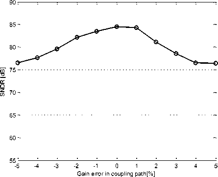
Fig. 12. SNDR variation with coupling path error
According to Figure 12, with ±5% error in the coupling path, SNDR of the modulator changes about 8 dB. The SNDR variation of the proposed modulator is low because the effect of coupling path error is reduced due to high gain of the resonator in the band of interest.
Reduction in the gain of the opamps that are used in the resonators results in increasing the noise at the modulator output. Therefore, it reduces the SNDR value of the proposed modulator. Figure 13 shows SNDR variation with opamp gain. Only the opamps gain of the resonator is considered because the noise caused by coupling path error at the modulator output is shaped by the same transfer function as the quantization noise. Therefore, it does not have significant effect on the resolution of the proposed modulator.
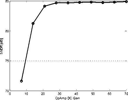
Fig. 13. SNDR variation with opamp gain
-20
-40
-60
Simulation shows that the proposed modulator is less sensitive to opamp gain variation. As shown in Figure 13, the SNDR is relatively constant with the different opamp gains. Figure 14 shows the histogram of the resonator output swing for the proposed modulator. By choosing suitable values for A and B coefficients, resonator output swing is reduced and the probability of unstable behavior is minimized. Also, this reduces the nonlinear effects in the modulator and therefore increases the SNDR value.
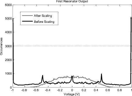
Fig. 14. Histogram of resonator output swing
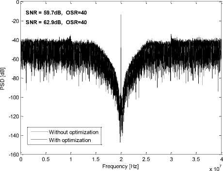
If the zero optimization technique is used in the proposed modulator, the SNDR of the modulator increases. Figure 15 is shown that the zero optimization technique moves the zeros of NTF to the optimum frequencies and increases the SNDR of the proposed modulator.
(a)
Without optimization With optimization
-80
-100
-120
-140
1.85 1.9 1.95 2 2.05 2.1 2.15
Frequency [Hz]
x 107
-160
(b)
Fig. 15. (a) Power spectral density of the proposed modulator; (b) Expanded view of PSD
Table 2 shows the simulation results of the proposed modulator. By considering the values in Table 2, the proposed 2-order noise coupled modulator is achieved SNDR = 85.35 dB at 80 MHz sampling frequency, 200 KHz bandwidth, and OSR = 200. The number of active elements that are used in the proposed modulator is less than previously reported modulators in the literatures. In Table 3, simulation results of the proposed modulator are compared with the other modulators.
Table 2. Simulation Results
|
Parameter |
Value |
|
Sampling Frequency |
80 MHz |
|
OSR |
200 |
|
Central Frequency |
20 MHz |
|
Bandwidth |
200 KHz |
|
Quantizer Bits |
1 |
|
Sampling Number |
65536 |
|
Maximum SNDR |
85.35 dB |
Table 3: Comparison Chart
|
Parameter |
Proposed modulator |
[27] |
[28] |
|
Order |
4 |
4 |
4 |
|
F s (MHz) |
80 |
20 |
80 |
|
OSR |
200 |
100 |
200 |
|
F c (MHz) |
20 |
5 |
20 |
|
BW(KHz) |
200 |
100 |
200 |
|
B |
1 |
1 |
1 |
|
Peak SNDR(dB) |
85.35 |
84.7 |
89.4 |
-
V. Conclusion
In a bandpass sigma-delta modulator, to have an N zero in the central frequency of the modulator, we need a 2N-order loop filter. This results in more power consumption and circuit complexity. In this paper, we used the noise coupling technique to reduce the order of loop filter and therefore power, and circuit complexity in bandpass modulator. Also, this technique resulted in reduction of nonlinear effect and improvement in the dynamic range of the modulator. To apply the noise coupling technique to a bandpass modulator, we need to implement Z-2 delay block but the proposed modulator was designed such that only needs Z-1 delay blocks. The simulation results of the proposed modulator were compared with the results of the conventional one and showed the resolution of the proposed modulator is slightly better. The proposed modulator was achieved 85.35 dB peak SNDR at -3 dBFS input amplitude in the 80 MHz sampling frequency and OSR=200.
References Filter Loop Reduction in DT BP Sigma-Delta Modulator Assisted by Noise Coupling Technique
- S. Norsworthy, R. Schreier, and G. Temes, “Delta-Sigma Data Converters: Theory, Design and Simulation”, IEEE Press, 1997, Institute of Electrical and Electronics Engineers, Inc., New York.
- R. Schreier and G. C. Temes, “Understanding Delta-Sigma Data Converters”, IEEE Press, 2004, J. Wiley & Sons Interscience, New York.
- J. Mitola, “The software radio architecture”, IEEE Communication Magazine, vol. 33, no. 5, pp. 26–38, May 1995.
- J. M. de la Rosa, “Sigma-Delta Modulators: Tutorial Overview, Design Guide, and State-of-the-Art Survey”, IEEE Transactions on Circuits And Systems—I: Regular Papers, January 2011, Vol. 58, No. 1, pp. 1 – 21.
- Kyehyung Lee, Jeongseok Chae, Mitsuru Aniya, Koichi Hamashita, Kaoru Takasuka, Seiji Takeuchi, and Gabor C. Temes, “A Noise-Coupled Time-Interleaved Delta-Sigma ADC With 4.2 MHz Bandwidth, 98 dB THD, and 79 dB SNDR”, IEEE Journal Of Solid-State Circuits, Vol. 43, No. 12, December 2008, pp. 2601-2611.
- Hyungil Chae, Jaehun Jeong, Gabriele Manganaro, Michael Flynn, “A 12mW Low-Power Continuous-Time Bandpass ΔΣ Modulator with 58dB SNDR and 24MHz Bandwidth at 200MHz IF”, IEEE International Solid-State Circuits Conference, San Francisco, CA , February 2012, pp. 148-150.
- Ramin Zanbaghi and Terri S. Fiez, “A Novel Low Power Hybrid Loop Filter for Continuous-Time Sigma-Delta Modulators”, IEEE International Symposium on Circuits and Systems, Taipei, May 2009, pp. 3114 – 3117.
- Hwi-Ming Wang and Tai-Haur Kuo, “The Design of High-Order Bandpass Sigma-Delta Modulators Using Low-Spread Single-Stage Structure”, IEEE Transactions on Circuits And Systems—II: Express Briefs, April 2004, Vol. 51, No. 4, pp. 202 – 208.
- Shu-Chuan Huang and Chia-Te Fu, “A Tunable SC Bandpass Delta-Sigma Modulator for Multi-Standard Applications”, IEEE Asia Pacific Conference on Circuits and Systems, Macao, 2008, pp. 1156 – 1159.
- Takaya Yamamoto, Masumi Kasahara, and Tatsuji Matsuura, “A 63 mA 112/94 dB DR IF Bandpass SD Modulator With Direct Feed-Forward Compensation and Double Sampling”, IEEE Journal of Solid-State Circuits, August 2008, Vol. 43, No. 8, pp. 1783 - 1794.
- Kyehyung Lee and Gabor C. Temes, “Enhanced split-architecture delta-sigma ADC”, IEEE International Conference on Electronics, Circuits and Systems, Nice, December 2006 , pp. 427 – 430.
- K. Lee and M. Bonu and G.C. Temes, “Noise-coupled delta sigma ADCs”, Electronics Letters, November 2006, Vol. 42, No. 24.
- K. Lee, G. C. Ternes, and F. Maloberti, “Noise-coupled multi-cell delta sigma ADCs”, IEEE International Symposium on Circuits and Systems, New Orleans, LA, May 2007, pp. 249-252.
- Y. Wang and G. C. Ternes, “Delta Sigma ADCs with second-order noise-shaping enhancement”, IEEE International Midwest Symposium on Circuits and Systems, Cancun, August 2009, pp. 345 - 348.
- Kyehyung Lee, Jeongseok Chae, Mitsuru Aniya, Kaoru Takasuka, Seiji Takeuchi, and Gabor C. Temes, “A Noise-Coupled Time-Interleaved Delta-Sigma ADC With 4.2 MHz Bandwidth, 98 dB THD, and 79 dB SNDR”, IEEE Journal of Solid-State Circuits, December 2008, Vol. 43, No. 12, pp. 2601 - 2612.
- Yan Wang and Gabor C, “Temes, Noise-Coupled Continuous-Time ΔΣ ADCs”, 52nd IEEE International Midwest Symposium on Circuits and Systems, August 2009, pp. 1 - 4.
- Y. Wang and G.C, “Temes, Noise-coupled continuous-time delta-sigma ADCs”, Electronics Letters, March 2009, Vol. 45 No. 6.
- Y. Jung, S. Lee, C. H. Chen and G.C. Temes, “Double noise coupling ∆Σ analogue-to-digital converter”, Electronics Letters, May 2012, Vol. 48, No. 10.
- H. San and H. Kobayashi, “Complex bandpass ΔΣAD modulator with noise-coupled architecture”, IEEE International Midwest Symposium on Circuits and Systems, Knoxville, TN, August 2008, pp. 486-489.
- H. San and H. Kobayashi, “Complex bandpass ΔΣAD modulator with noise-coupled image rejection”, IEEE International Midwest Symposium on Circuits and Systems, Cancun, August 2009, pp. 357-360.
- J. Silva, U. Moon, J. Steensgaard, and G. C. Temes, “Wideband lowdistortion ∆Σ ADC topology”, Electronics Letters, vol. 37, no. 12, pp.737–738, June 2001.
- A. K. ong, “Bandpass Analog-To-Digital Conversion For Wireless Applications”, Ph.D. dissertation, Stanford Electronics Laboratories, Stanford Univ., September 1998.
- Teemu Salo, “Bandpass Delta-Sigma Modulators for Radio Receivers”, Ph.D. dissertation, Department of Electrical and Communications Engineering, Helsinki University of Technology, April 2003.
- Franco Maloberti, “Data Converters”, Springer, 2007.
- Kyehyung Lee, Matthew R. Miller, and Gabor C. Temes, “An 8.1 mW, 82 dB Delta-Sigma ADC With 1.9 MHz BW and 98 dB THD”, IEEE Journal Of Solid-State Circuits, Vol. 44, No. 8, August 2009.
- Piero Malcovati, Simona Brigati, Member, Fabrizio Francesconi, Franco Maloberti, Paolo Cusinato, and Andrea Baschirotto, “Behavioral Modeling of Switched-Capacitor Sigma–Delta Modulators”, IEEE Transactions on Circuits And Systems —I: Fundamental Theory And Applications, Vol. 50, No. 3, March 2003.
- Hiva Hedayati And Sayyed Mahdi Kashmiri, “A 13 Bit Band-Pass Double-Sampling Delta-Sigma A/D Converter For 5 MHz IF Signals”, Canadian Conference on Electrical and Computer Engineering, Vol. 1, May 2003, pp. 65 – 68.
- X. Liuet, Honglin Xu, Jiajun Zhou, Song Chen, Jiang Yang, “An improved fourth-order band-pass sigma-delta modulator with a novel resonator”, IEEE International Conference on Optoelectronics and Microelectronics, August 2012, pp. 510 - 513.
