FPGA Based High Accuracy Synchronous Acquisition Design for Binocular Vision System

Author: Lili Lin, Wenhui Zhou
Journal: International Journal of Information Technology and Computer Science(IJITCS) @ijitcs
Article in issue: 3 Vol. 3, 2011.
Free access
This paper proposes a coarse-to-fine two-level synchronous data acquisition and transmission system for binocular stereo vision, which satisfies strict synchronous requirement of stereo vision. Specifically, this synchronization system design contains: coarse level synchronous based on hardware circuit design and the fine level synchronous based on hardware description language (HDL) design. The former includes the synchronization design of clock and external trigger. The latter utilizes a multi-level synchronous control strategy from field-level to pixel-level, which consists of field-synchronous acquisition of the two-channel video inputs, two-channel Ping-pong buffers switch control module, and pixel-synchronous bit-splicing and PCI transmission module. The experiments of synchronous acquisition and display demonstrate the high reliability and great performance of this synchronous system.
Binocular Stereo Vision, Synchronous Acquisition, Ping-pong Buffer, FPGA
Short address: https://sciup.org/15011622
IDR: 15011622
Text of the scientific article FPGA Based High Accuracy Synchronous Acquisition Design for Binocular Vision System
Published Online June 2011 in MECS
The techniques of stereo vision are used widely in many fields, such as stereo film / 3DTV [1], virtual reality [2], 3D modeling [3], robot navigation [4], and etc. Binocular stereo vision is the most basic and common stereo vision system, and it consists of stereo pairs acquisition, image rectification, stereo corresponding, 3D reconstruction and 3D display [5]. Stereo pairs acquisition is the crucial premise of stereo vision system, and it directly affects the subsequent processing. Its difficulty is how to implement real-time and high precision synchronous acquisition of the two-channel video signal [6]. Most existed multi-channel image capture cards are based on time-division operation or multi-branch switch, which can not satisfy the requirements of real-time synchronous acquisition of the two-channel or multichannel video.
We have designed and made a FPGA based binocular stereo vision acquisition system [7, 8]. On the basis of
This work is supported by the National Natural Science Foundation of China (60902077), and the National Natural Science Foundation of Zhejiiang Province (Y1091074) .
this work, we further propose a coarse-to-fine two-level synchronous technique: the hardware circuit based coarse level design and the hardware description language (HDL) based fine level design. The latter is our focus in this paper, and a field-to-pixel synchronous control strategy is proposed. Experiment results demonstrate the proposed synchronous binocular stereo acquisition system has high reliability and excellent performance.
-
II. Block Diagram of Hardware System
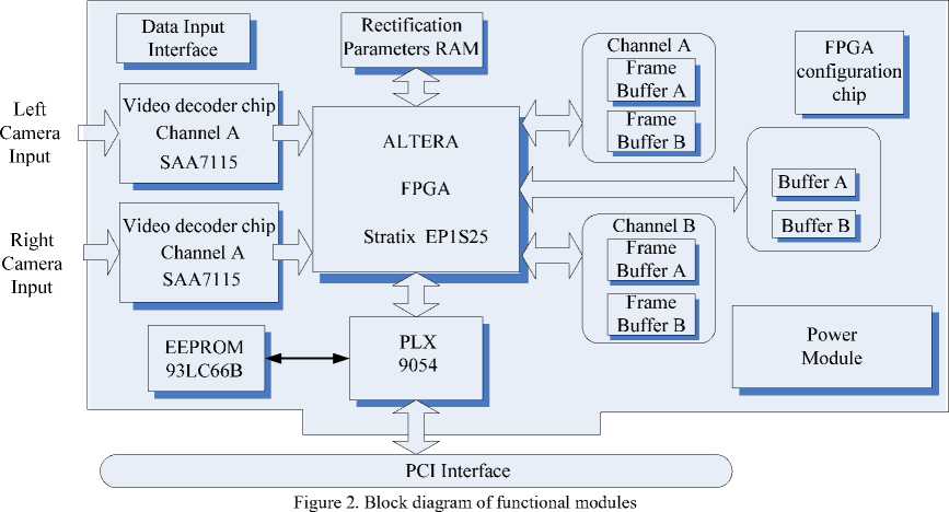
The whole hardware system is a 10-layer PCB board, as shown in Fig.1, and it can be partitioned into four modules in function, namely, video input module, video decoder module, PCI data transmission module, and video processing module. The input two-channel synchronous video signal is decoded by video decoder chip, and the output digital signal Y-CB-CR is written into the frame buffer of each channel. FPGA reads the image intensity data from frame buffer, and written them into the special buffer after geometry rectification. SRAM uses the Ping-pong buffer manipulation. And data is transferred to the computer by PCI bus. The functional module diagram of the hardware system is illustrated in Fig.2.
The key of the whole system is the synchronous acquisition and transmission of the video data from two cameras. The synchronous performance directly affects the accuracy and robustness of the follow-up stereo match algorithm. A two-level synchronous strategy based
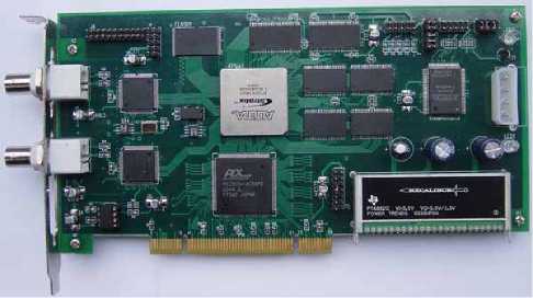
Figure 1. 10-layer PCB board of the hardware system
on software and hardware is proposed in this paper, and can achieve accurate synchronous acquisition and transmission in pixel-level.
-
III. Design Diagram of two-level synchronous Scheme
The two-level synchronous scheme consists of video decoder chips and its controller, clock synchronous circuit, SRAM and its Ping-pong buffer control, and PCI bus controller.
NXP Semiconductors' SAA7115 [9] video decoder chip is selected in our design, because it is a 9-bit video decoder with adaptive PAL/NTSC Comb Filter and a high performance scaler. It can realize horizontal and vertical down-scaling and up-scaling to randomly sized window. It supports multiple video standards, and can realize the control of intensity, contrast, and saturation. FPGA chip is Altera Company’s StratixTM EP1S25F780 [10]. It has about 25 thousands logic units, 1899K bits on-chip RAM and eighty 9-bit×9-bit hardware multipliers, so it satisfies the requirements of most stereo acquisition processing. Four 256K×16-bit SRAM chips CY7C1041CV33 of Cypress Company are selected as Ping-pong buffer. PCI bus controller is the PLX Company’s 32-bit PCI 9054 [11], which is compatible with PCI v2.2 specification. It has advanced data pipeline architecture and two dependent DMA channels. Its local bus clock and the burst transmission speed can achieve 50MHz and 132MB/s, respectively. In our hardware platform, the image transmission speed is about 46MB/s.
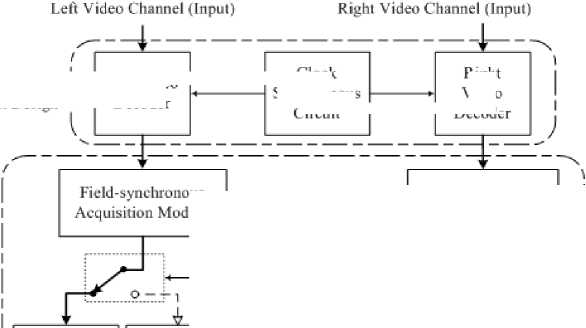
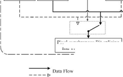
The main contribution of this paper is to propose a coarse-to-fine two-level synchronous acquisition system, which includes the synchronous designs of hardware circuit and HDL, and the diagram is shown in Fig.3. Hardware circuit synchronization is to implement the input clock synchronization of two-channel video decoders and the external trigger synchronization. While the HDL synchronization is to implement the field- synchronous acquisition of the two channels video inputs, two-channel Ping-pong buffer switch control module, and pixel-synchronous bit-splicing and transmission.
-
IV. Synchronous Design of Hardware circuit
The synchronous design of hardware circuit includes two video acquisition channels, clock synchronous circuit, and two Ping-pong buffer channels. The hardware diagram and the clock synchronous circuit are shown in Fig.4.
To ensure the synchronous decoding of the two-channel video signal, two video decoders SAA7115 have the same configuration parameters. The image resolution is 320×240, and the video decoding data format is YCrCb 4:2:2. Four SRAMs are divided into two group buffers and used as Ping-pong buffers for video acquisition. Synchronous switch control strategy is adopted between the two group Ping-pong buffers.
By zero delay buffer CY2305, clock synchronous circuit divides the output of crystal oscillators into two synchronous clocks, which are used as the input clocks of two SAA7115 chips. To reduce the delay offset between these input clocks, the matched length rules must be kept during the clock routing.
-
V. Synchronous Design of HDL
The aim of HDL synchronous design is to implement the field-to-pixel synchronization. Following the modular design idea, the HDL synchronous system can be partitioned into field-synchronous acquisition module, two-channel Ping-pong buffer switch control module, and pixel-splicing and transmission module. Each module is described by Verilog HDL, and the online timing logic verification is done by the online logic analyzer embedded in the Quartus II. For the module whose timing logic is difficult to observe online, we use the ModelSim to perform function simulation.
Right
Decoder
Left Frame Buffer A
Fi eld- synchronous Acquisition Module
Left Frame Buffer В
Two-channel Ping-pong Buffer Switch Control Module
Synchronous |
Circuit Design I
Synchronous HDL Design
Left Video
Decoder
Clock Synchronous Circuit
Right Frame
Buffer A
Right Frame
Buffer В
Control Signal Flow
Spliced Data
Figure 3. Diagram of the synchronous acquisition system Signal Flow
Pixel-synchronous Bit-splicing and Transmission Module
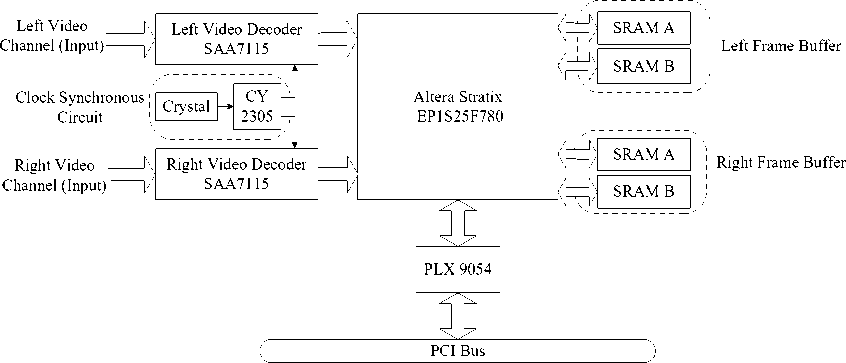
Figure 4. Diagram of hardware system and the clock synchronous circuit
-
A. Field-synchronous acquisition module
In this module, two-channel video data are acquired field-synchronously, and written into the corresponding buffers. The output pixel clock of SAA7115 is used as sampling clock. When the field synchronization signal of SAA7115 is valid, the two-channel video data are captured and written to the buffers simultaneously. After
capturing a field of video data, Ping-pong buffer switch is performed according to the synchronous signal RAM_RWEN of the two-channel Ping-pong buffer switch control module, and waiting for the synchronization signal of next field. Repeat this process until the field-synchronous acquisition of the two-channel video is finished.
When video data are written into the buffer, the YC b C r data of each output pixel of SAA7115 are spliced to a 16-bit data and written into the Ping-pong buffer, where Cb or C r is written in the upper-byte, and Y in the lower-byte. Fig.5 is the timing logic of writing video data to buffer, captured by the Quartus II TimeQuest timing analyzer. When the data valid signal S7115A_IDQ is enabled, the data bus S7115A_IPD has four 8-bit valid data (two pixels). Namely, Cb=0x7FH, Y=0x19H, and Cr=0x82H, Y =0x13H. The spliced data 0x7F19H and 0x8213H are written to address 0x12BFFH and 0x12C00H, respectively. At the end of the current field signal, the synchronous signal RAM_RWEN is inverted to perform Ping-pong switch. In Fig.6, LCCDA_NCE, LCCDA_NOE and LCCDA_NWE are chip-selection, read enable, and write enable signals, respectively. They are all low voltage effective.
The interface program of SAA7115 is followed.
-
--read data from the left camera 7115A_Reg[].d = 7115A_IPD[]; 7115A_Reg[].clk = 7115A_ICLK;
7115A_Reg[].ena = 7115A_IDQ & 7115A_IGPH & 7115A_IGPV & 7115A_IGP0;
-
--assemble SAA7115A's data and SAA7115B's data into 16-bit at next 7115A_ICLK
LeftCCD_Reg[].d =
(LeftCCD_Reg[7..0],7115A_Reg[]);LeftCCD_Reg[].clk = 7115A_ICLK;
LeftCCD_Reg[].ena = 7115A_IGPH & 7115A_IGPV & 7115A_IGP0;
-
B. Two-channel Ping-pong buffer switch control module
The design of Ping-pong buffer can satisfy the requirements of pipeline acquisition, transmission and real-time processing of videos. For the two-channel video acquisition, this paper proposes the two-channel Pingpong buffer architecture and the synchronous Ping-pong control module. The synchronous switch and control of two-channel Ping-pong depend on the synchronous signal RAM_RWEN.
Two-channel Ping-pong buffer switch control module is the core of binocular vision synchronous acquisition and transmission. As shown in Fig.3, this module controls the two-channel Ping-pong switch by the synchronous signal RAM_RWEN, and ensures the switch from coarse field-synchronization to fine pixelsynchronization in the Ping-pong buffer.
In practical system, it is difficult to achieve accurate field synchronous. The generation of RAM_RWEN is the key of the whole synchronous control. Since the external trigger of clock synchronization and field synchronization is guaranteed by the hardware circuit synchronous design, we only need detect the descend edge of the field end signal, and take it as the flip trigger signal of RAM_RWEN.
Because the time scope observed by the Quartus II online logic analyzer is limited and the difference between the delays of actual two-channel field synchronous signal is bigger, it is hard for online logic analyzer to simultaneously observe the descend edge of the two-channel field synchronous signal. This paper uses ModelSim to perform the timing logic simulation of this module, and the timing is shown in Fig.4. When the descend edges of the left and right channel field synchronous signal S7115A_IGPV and S7115B_IGPV are detected, the corresponding flags AFLAG and BFLAG are set to high voltage, then the Ping-pong switch control signal is inverted, and AFLAG and BFLAG are set to low voltage to wait for the next field switch.
|
Type |
Alias |
Name | |
|
S7115AJDQ |
||
|
0 S7115AJPD |
||
|
0- LCCDA_ADDR |
||
|
0 LCCDA_DATA |
||
|
■_z |
LCCDA.NWE |
|
|
■_z |
LCCDA_NCE |
|
|
■_z |
LCCDA_NOE |
|
|
RAM_RV/EN |
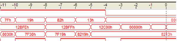
Figure 5. The timing of field synchronous acquisition module
4 /test/CLK_5OMHZ
4 /test/S7115A_IGPV
4 /test/uut/S7115A_IGPV_Dl
4 /test/uut/S7115A_IGPV_D2
4 /test/uut/AFLAG
4 /test/S7115B_IGPV
4 /test/uut/S7115B_IGPV_Dl
4 /test/uut/S7115B_IGPV_D2
4 /test/uut/BFLAG
О
О
О
О
О
О
О
О
О
+ /test/uut/RAM RWEN
Figure 6. Simulation timing of two-channel Ping-pong buffer switch control module
To guarantee the stable detection of the descend edge of field signal, the deburring design is used in this module. Take the descend edge detection of left channel field signal S7115A_IGPV for example, there are two delay registers S7115A_IGPV_D1 and S7115A_IGPV_D2, and they are assigned values on the rising edge of system clock to implement one and two clock delays, respectively. When the rising edge trigger detects the value of S7115A_IGPV_D1 and S7115A_IGPV_D2 are 1and 0, respectively, the flag bit AFLAG is set to high.
-
C. Pixel-splicing and transmission module
The synchronous pixel-splicing of the two-channel video data is implemented in this module, and the spliced 32-bit data flows are transmitted to the computer by PCI bus. When transmission module receives the read request signal from PCI 9054, FPGA selects the corresponding SRAM in Ping-pong buffer to read according to the synchronous signal RAM_RWEN. Two-channel 16-bit data are read out from the same address of the two-channel buffer, and are spliced into 32-bit data, where the
left and right channel video data are the low 16-bit and high 16-bit, respectively. Since the data are read out from the same address, the two-channel 16-bit data have the same image coordinate, and thus realize the pixel level synchronous transmission of the two-channel video.
To make it easy to incorporate the subsequent image rectification and match algorithms, this paper utilizes the finite state machine to accomplish the read-write timing, as shown in Fig.7. This state machine has seven states, and they are idle, start, single cycle start, single cycle termination, burst start, burst waiting, and burst termination. These seven states are corresponding to the idle, start, single transmission pattern waiting, single transmission pattern termination, burst transmission pattern waiting, burst transmission pattern repetition, burst transmission pattern termination, respectively. NADS and NBLAST signals are valid address signal and the burst last transfer signal, respectively. They are asserted by PCI 9054, and low voltage effective.
And the AHDL program of the state machine is listed below.
NADS is high
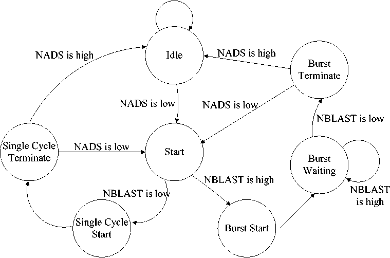
Figure 7. Read and write state machine of PCI 9054
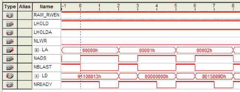
Figure 8. The read timing of PCI 9054
case PCIState is when S_PCI_Idle => if(!9054_NADS) then
PCIState = S_PCI_Ready;
else
PCIState = S_PCI_Idle;
-
end if;
when S_PCI_Ready => if(!9054_NBLAST) then
PCIState = S_PCI_Single;
elsif(9054_NBLAST) then
PCIState = S_PCI_BurstReady;
else
PCIState = S_PCI_Idle;
-
end if;
when S_PCI_Single =>
PCIState = S_PCI_End;
when S_PCI_BurstReady =>
PCIState = S_PCI_Burst;
when S_PCI_Burst => if(!9054_NBLAST) then
PCIState = S_PCI_BurstEnd;
else
PCIState = S_PCI_Burst;
-
end if;
when S_PCI_BurstEnd =>
PCIState = S_PCI_End;
when S_PCI_End => if(!9054_NADS) then
PCIState = S_PCI_Ready;
else
PCIState = S_PCI_Idle;
-
end if;
when others =>
PCIState = S_PCI_Idle;
end case
The PCI read timing logic captured by the Quartus II online analyzer is shown in Fig.8, where LHOLD is asserted by PCI 9054 to request the local bus. LHOLDA is request acknowledge signal. When PCI 9054 receives LHOLDA, it drives the bus and continues the transfer.
NLWR is PCI write/read control signal. It asserted high for read, and asserted low for write. NREADY is read / write data bus valid signal, it is asserted low for valid data will be present on the bus LD.
-
VI. Experiments and results
We carried out two set experiments to verify the performance of the synchronous system designed by us, and the hardware platform is the self-made binocular stereo vision capture card shown in Fig.1.
The first set of experiment is to synchronously acquire binocular stereo video and display them on the LCD screen. The video display speed equals the frame rate of binocular video acquisition, and is 25 frames per second. The spliced 32-bit data are transmitted to the computer by PCI bus. Then the computer program retrieves the left and right images from the high 16-bit data and the low 16-bit data, respectively.
In Fig.9, (a) and (b) are the left and right image pairs captured at the same time. Experiment results indicate the acquired left and right images at any time are the same frame of the left and right video.
The second set of experiment is to capture a CRT display whose refresh rate is 60Hz in binocular synchronous fashion. Since the CRT display is progressive scanning, the scan frequency and sampling frequency are mismatched. Therefore, a highlight horizontal scroll bar caused by the fly back of electron gun can be observed in the captured video sequences. Experiment results demonstrate the highlight scroll bars always locate at the same position in the left and right images captured at any time, as illustrated by Fig.10.
The above experiment results demonstrate the proposed pixel level binocular synchronous acquisition and transmission system possess high reliability and good performance.
The work of this paper is the premise and guarantee of the implementation of embedded binocular stereo vision system. In this paper, we use the modular design method, which make it easy to incorporate subsequent module, such as geometric rectification, stereo match, and etc. Future work will focus on implementing FPGA based stereo vision modules.
References FPGA Based High Accuracy Synchronous Acquisition Design for Binocular Vision System
- O. Schreer, C. Fehn, N. Atzpadin, etc. “A Flexible 3D TV System for Different Multi-Baseline Geometries,” IEEE International Conference on Multimedia and Expo, 1877-1880, 2006
- P. Zemcik, “Hardware acceleration of graphics and imaging algorithms using FPGAs,” 18th Spring Conference on Computer Graphics, pp.25-32, 2002.
- D. Chaikalis, N.P. Sgouros and D. Maroulis. “A real-time FPGA architecture for 3D reconstruction from integral images,” Journal of Visual Communication and Image Representation, vol. 21, no. 1, pp. 9-16, 2010
- Wen-Chung Chang, Shu-An Lee. “Real-time feature-based 3D map reconstruction for stereo visual guidance and control of mobile robots in indoor environments,” IEEE International Conference on Systems, Man and Cybernetics, vol. 6, no.7, pp. 5386-5391, 2004.
- M.Z. Brown., D. Burschka and G..D. Hager, “Advances in computational stereo,” IEEE Transactions on Pattern Analysis and Machine Intelligence, vol. 25, no. 8, pp. 993-1008, 2003.
- S. Wong, S. Vassiliadis and S. Cotofana. “A sum of absolute differences implementation in FPGA hardware,” the 28th EUROMICRO Conference, Dortmund, Germany, pp.183-188, 2002
- Wenhui Zhou, Xin Du, Xiuqing Ye. “FPGA based binocular stereo vision system (in Chinese),” Journal of Image and Graphic, vol. 10, no.9, pp. 1166-1170, 2005.
- Min Ye, Wenhui Zhou, Weikang Gu. “FPGA based real-tim image filter and edge detection (in Chinese),” Chinese Journal of Sensors and Actuators, vol. 20, no. 3, pp. 623-627, 2007.
- NXP Semiconductors. SAA7115: PAL/NTSC/SECAM video decoder with Adaptive PAL/NTSC Comb Filter, High Performance Scaler, I2C Sliced Data Readback and SQ Pixel Output. 2002
- Altera Corporation. Stratix Device Handbook, Volume 1 & 2. Version 3.5. June 2006
- PLX Technology. PCI 9054 Date Book. Version 2.1. January 2000.
