Fredkin circuit in nanoscale: a multilayer approach

Author: Abdullah-Al-Shafi, Ali Newaz Bahar
Journal: International Journal of Information Technology and Computer Science @ijitcs
Article in issue: 10 Vol. 10, 2018.
Free access
Nanotechnologies, exceedingly Quantum-dot Cellular Automata (QCA), presents a notable perception for upcoming nanocomputing. Feature extent of circuits is moving to sub-micron point that produces the sophisticated device intricacies. In this work, QCA is considered as an application technique for reversible logic. A multi-layer reversible Fredkin circuit is proposed with QCA nanotechnology. The accomplishment of the outlined circuit is substantiated with five existing Fredkin gate, which exhibits from 71.20% to 37.50% improvement in term of cell intricacy. The proposed design uses 55 cells concerning only 0.03 μm2 area and latency is 0.75. The power consumption by the proposed circuit is also presented in this literature. The proposed design has been realized with QCADesigner version 2.0.3.
Quantum-dot Cellular Automata (QCA), Fredkin Gate, QCADesigner, Energy dissipation
Short address: https://sciup.org/15016305
IDR: 15016305 | DOI: 10.5815/ijitcs.2018.10.05
Text of the scientific article Fredkin circuit in nanoscale: a multilayer approach
Published Online October 2018 in MECS
Due to the exponential diminution in element size in CMOS archetype, devices are further disposed to extreme leakage current and power dissipation. In accordance with Moore's law [1], every 18 months the measure of transistors that could be cohesive into a particular chip is doubled that causes in saving area and lessening device magnitudes. In this outlook, quantum-dot cellular automata (QCA) is the appropriate nominee that has not any of the mentioned complications and abilities particularly minimal power dissipation with small magnitude feature and high switching frequency [2]. Landauer [3] presented that, irrespective of the underlying technology, typical logic circuits deplete heat in an order of kTln2 joules for every bit of information that is dropped. Afterward, Bennett [4] established that if computations are executed devoid of abolishing the information then rationally zero dissipation is possible. Because of favorable assets like minimal extent, extreme packing thicknesses and lower signal interruptions, QCA has achieved consideration in recent times. It was initially outlined in binary formula, however, multi-valued logic (MVL) which offers rapid implementation and inputs/outputs fall [5]. Besides, reversibility in a quantum computing is outlined a bijective relation concerning inputs to outputs that directs to minimize power dissipation. Rest of the literature is prepared as follows: Section 2 represents the synopsis of QCA and reversible logic. Section 3 signifies the proposed multi-layer Fredkin gate. The comprehensive comparison of the proposed gate with the existing designs are organized in Section 4. Overall power dissipation by the outlined circuit is discussed in Section 5. Lastly, conclusions are pointed in Section 6.
-
II. Summary: Background of Binary QCA
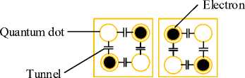
The binary quantum-dot is a four-sided cell alongside four quantum dots engaging the four apexes of the cell. Every single cell embraces two additional charges and the electrons can channel between dots and ultimately subjugate the antipodal locations due to Coulombic repulsion to complete minimal area [2]. Based on repulsion law of Coulomb, two electrons can individually engage antipodal positions in the cell. Therefore, each cell can encompass polarization status of either P = +1 or P = -1 with binary states 1 and 0, individually are explained in Figure 1.
P= + 1 P= -1
Fig.1. Four dotted QCA cell with binary encoding
The QCA assemblies of the essential gates are illustrated in Figure 2 to 4; specifically, QCA wire, majority voter and the inverter. QCA wires can be either made up of 45o cells or 90o cells. These cells used to transmit binary data from one side to another. Three input majority voter (Maj3) is the fundamental logic gate in QCA which can be comprised by five QCA cells where three used as inputs, one is output and another is the unique middle cell. The middle cell sometimes familiar as device cell that shifts to principal polarization [6] and determines the stable output. Quite a few designs based on basic building blocks of QCA are organized in [7-26]. The logical equation of Maj3 is as follows:
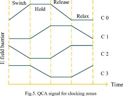
Clock signals for every single state are different and 90o phase shifted. The clocking flow is presented in Figure 5. Two particular kinds of crossover approach usually used in QCA circuit specifically, coplanar and multilayer. Multilayer crossover utilizes more than one layer of QCA cells, whereas coplanar crossover uses two separate cells for wire-crossing. In this study, multi-layer approaches are utilized [28].
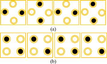
Fig.2. QCA wire (a) 45o (b) 90o
MV (A, B, C) = AB+BC+CA (1)
B=1
Maj Output=1

Fig.3. Fundamental form of 3-input majority voter gate
The QCA inverter basically transmits the cell polarization to the reverse polarization as presented in Figure 4. QCA circuits require apposite clocking to switch the flow of information that also supports essential power to operate the circuit. To operate the input to the anticipated output, signals need to be conceded through four stable clock zones [27] namely, Relax, Switch, Hold, and Release.
Reversible logic accomplishes the reversible purpose where the output shapes can be utilized to recuperate input outlines by reason of one to one mapping. Orthodox logic circuits cannot reinstate the inputs from the generated outputs, defined to as reversibility. In this phase, reversible computing in the field of nanotechnology, specifically, quantum computing, widespread studies have been considered. Two methodologies are there to realize reversibility: substantial reversibility and logical reversibility. Substantial reversibility indicates that there must be some requirements for computation in opposite manner. Logical reversibility defines bijective relation between outputs and inputs, thus inputs can be reasoned from the outputs. A number of efforts to implement reversible circuit have been completed in many scientific papers [10, 12-14, 18-23, 25, 26, 29]. Moreover, parity-conserving reversible circuits were designed in [30] for identifying inaccuracies in reversible circuits.
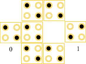
Fig.4. Seven cell QCA inverter
III. Proposed Fredkin Gate in QCA
Fredkin circuit is a 3×3 reversible logic circuit [31]. The stable input A, B and C to Fredkin circuit have distinctive output as P =AB+ A', Q = A'B+ AC and R = A. Its quantum charge is five [26]. The appropriate truth table is presented in Table 1 and majority voter-based equation of Fredkin circuit consistent to truth table as explained in Table 1 can be obtained as
Table 1. Truth Table of proposed Fredkin circuit
Input Output
|
A |
B |
C |
P |
Q |
R |
|
0 |
0 |
0 |
0 |
0 |
0 |
|
0 |
0 |
1 |
1 |
0 |
0 |
|
0 |
1 |
0 |
0 |
1 |
0 |
|
0 |
1 |
1 |
1 |
1 |
0 |
|
1 |
0 |
0 |
0 |
0 |
1 |
|
1 |
0 |
1 |
0 |
1 |
1 |
|
1 |
1 |
0 |
1 |
0 |
1 |
|
1 |
1 |
1 |
1 |
1 |
1 |
P = mv(mv(A, B, 0), mv(A', C, 0), 1) (2)
Q = mv(mv(A', B, 0), mv(A, C, 0), 1) (3)
R = A (4)
The designed QCA structure of Fredkin circuit is presented in Figure 6 and QCA outline is in Figure 7. The proposed circuit is realized with only three majority voters and one inverter. Simulation result of designed gate is showed in Figure 8. Figure 8 establishes that for series of fixed inputs (A, B, C) as (0, 0, 0), the related series of outputs (P, Q, R) will be (0, 0, 0). For series of inputs (A, B, C) as (0, 0, 0), the relevant series of outputs (P, Q, R) will be (1, 0, 0). Correspondingly, for all input patterns, consistent results are presented in Figure 8. The results and the speculative values of Fredkin circuit as presented in Table 1 are equated which assesses the computation suitability of the proposed circuit.
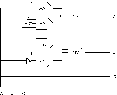
Fig.6. Proposed layout of Fredkin gate in QCA
The designed model has been functionally simulated with the QCADesigner ver. 2.0.3. Successive parameters in the bistable approximation and coherence vector simulation are employed which are the default forms in QCADesigner. These parameters are listed as: size of cell 18nm, temperature 1K, dot diameter, 5.0, samples number 12800, time step 1.0e-16, convergence tolerance 0.001, relaxation time 1.0e-15, radius of effect 65 nm, clock amplitude factor 2, relative permittivity 12.900000, layer separation 11.50, clock low 3.80e–023, clock high 9.80e–022, concentrated iterations per sample 100.
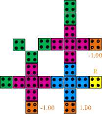
Layer 2

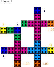
Main layer
Fig.7. QCA simulated circuit design of proposed Fredkin gate max: 1.00e+000 A min: -1.00e+000
max: 1.00e+000 C min: -1.00e+000
max: 1.00e+000 B min: -1.00e+000
max: 9.57e-001 P min: -9.59e-001
max: 9.26e-001 R min: -9.26e-001
max: 9.57e-001 Q min: -9.59e-001
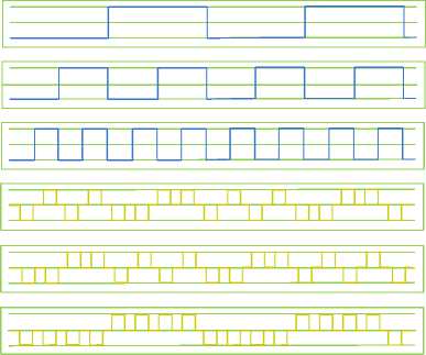
Fig.8. Simulated waveform for Fredkin gate
-
IV. Intricacy Study and Comparison Analysis of Proposed Fredkin Circuit
The hardware complications of the outlined design are organized in Table 2. From the table, it is perceived that the proposed Fredkin circuit requires three majority gate and single inverter. Number of cell required to design the gate is 55, and the area utilized by Fredkin gate is 0.03 µm2. The cell extent of Fredkin gate is 0.018 µm2 which outcomes in 60% area use regarding the overall extent.
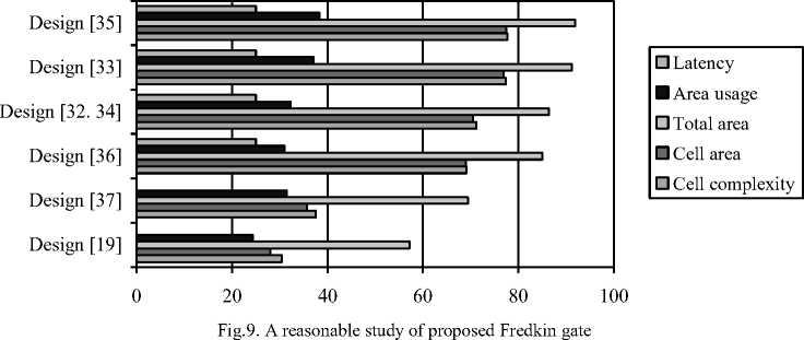
The outlined QCA design of Fredkin circuit is compared with the existing designs [19, 32–37] as presented in Table 2. The outlined Fredkin circuit has 30.38, 28 and 57.14% enhancements over [19] in terms of figure of cell, cell area, and total area, correspondingly, while over [36], the enhancements are 69.10, 68.97, 85 and 25%, in terms of overall cell, cell area, total area and latency respectively. Likewise, other enhancements are assessed and presented in Figure 9. The assessment evidently defines that the outlined circuit is faster and enhanced than that of the existing ones.
Table 2. Performance criterions of proposed circuit
|
Parameter |
Proposed |
Design in [19] |
Design in [37] |
Design in [36] |
Design in [32, 34] |
Design in [33] |
Design in [35] |
|
Cell intricacy |
55 |
79 |
88 |
178 |
191 |
243 |
246 |
|
Cell area (µm2) |
0.018 |
0.025 |
0.028 |
0.058 |
0.061 |
0.078 |
0.080 |
|
Total area (µm2) |
0.03 |
0.07 |
0.098 |
0.2 |
0.22 |
0.34 |
0.37 |
|
Area usage (%) |
60 |
35.71 |
28.58 |
29 |
27.72 |
22.94 |
21.62 |
|
Latency |
0.75 |
0.75 |
0.75 |
1.0 |
1.0 |
1.0 |
1.0 |
-
V. Power Dissipation by Proposed Circuit
Power dissipation assessment is a vital aspect in QCA circuit [38]. This part presents the overall power depletion by the designed circuit. The procedure organized in [39] is utilized to realize the depleted energy by the designed circuit in this study. The total depleted energy by any QCA circuit is deviated based on the utilized majority gate along with the number of used inverters [39].
Because of intrinsic nature, every single QCA cell in a circuit has consistent power depletion. Power consumption of QCA circuit will be elevated if the number of inverters and majority voter is raised. During a single clock cycle, the dissipated energy by any QCA layout can be estimated by accumulating the power consumption of all inverters as well as majority gates.
Hamming distances between input variation to majority gate and to inverter are used to estimate their power dissipations [39]. The assessment is completed at several levels of channeling energy. The functional temperature is measured at T = 2 K. The estimation outcomes corresponding to Table 3 is surveyed in Figure 10. The symbolizations T, γ, E k are utilized to characterize the temperature in which the procedure is carried out, channeling energy, and kink energy, correspondingly.
The competence of the proposed design under thermal unpredictability is verified in this study. To verify the proficiency, the polarization outcome on each output cell at several temperatures is perceived [40]. The results are presented in Figure 11 which clarifies that by growing the temperature, the average output polarization (AOP) for every single output of the proposed circuit is reduced.
Table 3. Power dissipation by proposed circuit at T=2 K
|
Design |
Power depletion |
|||
|
γ =0.25 E k |
γ =0.50 E k |
γ =0.75 E k |
γ =1.0 E k |
|
|
Fredkin gate |
98.3 |
101.8 |
107.3 |
113.6 |
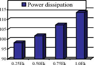
Fig.10. Power dissipation by the proposed Fredkin gate
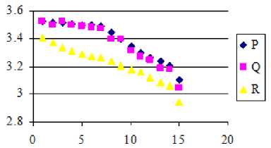
Fig.11. Temperature influence of the proposed circuit
The circuit executes competently up to temperature T = 14 K and after this temperature, the AOP of every output is very minimal, and the signals reduce. QCA Designer is utilized to attain AOP for every single output cell. For instance, the highest and lowest polarization for output cell ‘Q’ of proposed circuit is 9.57e–001 and -9.59e–001 at temperature T = 1 K, correspondingly. Therefore, the AOP for output cell ‘OUT’ is calculated as [(highest polarization+ lowest polarization)/2=] 3.524 as presented in Figure 11.
-
VI. Conclusion
In nanoscale logic design, device density and heat depletion are the perplexing concerns. QCA and reversible logic together can resolve these issues. In this literature, an efficient reversible Fredkin logic gate is proposed. We survey the performance of the proposed circuit and then compared with the existing layouts. The designed Fredkin circuit is faster and improved than that of the previous models and offered considerably enhancement overall measured metrics for example extent, cell extent, delay and complexity. Besides the power depletion and reliability of the proposed circuit is reported. Energy depletion by the proposed circuit indicates that the design depletes minimum energy. The assessment of simulation outcome with truth table defines the design precision of the circuit.
References Fredkin circuit in nanoscale: a multilayer approach
- Nanotechnologies, exceedingly Quantum-dot Cellular Automata (QCA), presents a notable perception for upcoming nanocomputing. Feature extent of circuits is moving to sub-micron point that produces the sophisticated device intricacies. In this work, QCA is considered as an application technique for reversible logic. A multi-layer reversible Fredkin circuit is proposed with QCA nanotechnology. The accomplishment of the outlined circuit is substantiated with five existing Fredkin gate, which exhibits from 71.20% to 37.50% improvement in term of cell intricacy. The proposed design uses 55 cells concerning only 0.03 μm2 area and latency is 0.75. The power consumption by the proposed circuit is also presented in this literature. The proposed design has been realized with QCADesigner version 2.0.3.
- R. R. Schaller, “Moore's law: past, present and future”, IEEE spectrum, vol. 34, no. 6, pp. 52-59, 1997.
- C. S. Lent, P. D. Tougaw, W. Porod and G. H. Bernstein, “Quantum cellular automata”, Nanotechnology, vol. 4, no. 1, p. 49, 1993.
- R. Landauer, “Irreversibility and heat generation in the computing process”, IBM J. Res. Dev, vol. 5, no. 3, pp. 183–191, 1961.
- C. H. Bennett, “Logical reversibility of computation”, IBM J. Res. Dev, vol. 17, no. 6, pp. 525–532, 1973.
- M. Mohammadi, A. Niknafs and M. shghi, “Controlled gates for multi-level quantum computation”, Quantum Inf Process, vol. 10, no. 2, pp. 241–256, 2011.
- I. Amlani, A. Orlov, G. Toth, G. H. Bernstein, C. S. Lent, and G. L. Snider, “Digital Logic Gate Using Quantum-dot Cellular Automata”, Science, vol. 284, no. 5412, p. 289-291, 1999.
- A. N. Bahar, M.S. Uddin, Md. A. A. Shafi, M. M. R. Bhuiyan and K. Ahmed, “Designing efficient QCA even parity generator circuits with power dissipation analysis”, Alexandria Engineering Journal, 2017, in press.
- Md. A. A. Shafi, A. N. Bahar, M. A. Habib, M. M. R. Bhuiyan, F. Ahmad, P. Z. Ahmad and K. Ahmed, “Designing Single Layer Counter in Quantum-dot Cellular Automata with Energy Dissipation Analysis”, Ain Shams Engineering Journal, 2017, in press.
- Md. A. A. Shafi, A.N. Bahar, M. M. R. Bhuiyan, S. M. Shamim and Kawsar Ahmed, “Average output polarization dataset for signifying the temperature influence for QCA designed reversible logic circuits”, Data in Brief, vol. 19, pp. 42-48, 2018.
- Md. A. A. Shafi and A. N. Bahar, “Ultra-Efficient Design of Robust RS Flip-flop in Nanoscale with Energy Dissipation Study”, Cogent Engineering, Vol. 4, No. 1, pp. 1391060, 2017.
- M. K. Hassan, N. M. Nahid, A. N. Bahar, M. M. R. Bhuiyan, Md. A. A. Shafi and K. Ahmed, “Dataset demonstrating the temperature effect on average output polarization for QCA based reversible logic gates”, Data in Brief, vol. 13, pp. 713-16, 2017.
- Md. A. A. Shafi, A. N. Bahar, F. Ahmad and K. Ahmed, “Performance Evaluation of Efficient Combinational Logic Design Using Nanomaterial Electronics”, Cogent Engineering, vol. 4, No. 1, pp. 1349539, 2017.
- Md. A. A. Shafi and A. N. Bahar, “A Novel Binary to Grey and Grey to Binary Code Converter in Majority Voter-Based QCA Nanocomputing”, Journal of Computational and Theoretical Nanoscience, vol. 14, no. 5, pp. 2416-2421, 2017.
- P. K. Biswas, A. N. Bahar, M. A. Habib and Md. A. A. Shafi, “Efficient Design of Feynman and Toffoli Gate in Quantum dot Cellular Automata (QCA) with Energy Dissipation Analysis”, Nanoscience and Nanotechnology, vol. 7, no. 2 pp. 27-33, 2017.
- Md. A. A. Shafi, A. N. Bahar, F. Ahmad, M. M. R. Bhuiyan and K. Ahmed, “Power analysis dataset for QCA based multiplexer circuits”, Data in Brief, vol. 11, pp. 593-96, 2017.
- A. N. Bahar, F. Ahmad, N. M. Nahid, K. Hasan, Md. A. A. Shafi and K. Ahmed, “An optimal design of conservative efficient reversible parity logic circuits using QCA”, International Journal of Information Technology, 2018, in press.
- Md. A. A. Shafi and A.N. Bahar, “Optimized design and performance analysis of novel comparator and full adder in nanoscale”, Cogent Engineering, vol. 3, no. 1, pp. 1237864, 2016.
- Md. A. A. Shafi and A. N. Bahar, “Novel Binary to Gray Code Converters in QCA with Power Dissipation Analysis”, International Journal of Multimedia and Ubiquitous Engineering, vol. 11, no. 8, pp. 379-396, 2016.
- Md. A. A. Shafi, “Analysis of Fredkin Logic Circuit in Nanotechnology: An Efficient Approach”, International Journal of Hybrid Information Technology, vol. 9, no. 2, pp. 371-380, 2016.
- Md. A. A. Shafi, “Synthesis of Peres and R Logic Circuits in Nanoscopic Scale”, Communications on Applied Electronics, vol. 4, no. 1, pp. 20-25, 2016.
- Md. S. Islam, Md. A. A. Shafi and A. N. Bahar, “A New Approach of Presenting Universal Reversible Gate in Nanoscale”, International Journal of Computer Applications, vol. 134, no. 7, pp. 1-4, 2016.
- Md. S. Islam, Md. A. A. Shafi and A. N. Bahar, “Implementation of Binary to Gray Code Converters in Quantum Dot Cellular Automata”, Journal on Today’s Ideas -Tomorrow’s Technologies, vol. 3, no. 2, pp. 145-160, 2015.
- Md. A. A. Shafi and A. N. Bahar, QCA: An Effective Approach to Implement Logic Circuit in Nanoscale”, 5th International Conference on Informatics, Electronics & Vision (ICIEV), Dhaka, Bangladesh, pp. 620-624, 2016.
- Md. A. A. Shafi and A. N. Bahar, “Energy Optimized and Low Complexity 2-Dimensional 4 Dot 2 Electron Flip-flop and Quasi Code Generator in Nanoscale”, Journal of Nanoelectronics and Optoelectronics, vol. 13, no. 6, pp. 856-863, 2018.
- Md. A. A. Shafi, A. N. Bahar and Md. S. Islam, “A Quantitative Approach of Reversible Logic Gates in QCA”, Journal of Communications Technology, Electronics and Computer Science, vol. 3, pp. 22-26, 2015.
- Md. A. A. Shafi, Md. S. Islam and A. N. Bahar, “A Review on Reversible Logic Gates and its QCA Implementation”, International Journal of Computer Applications, vol. 128, no. 2, pp. 27-34, 2015.
- D. A. Antonelli, D. Z. Chen, T. J. Dysart, X. S. Hu, A. B. Kahng, P. M. Kogge, R. C. Murphy and M. T. Niemier, “Quantum-Dot Cellular Automata (QCA) Circuit Partitioning: Problem Modeling and Solutions”, Design Automation Conference (DAC), ACM, pp. 363–368, 2004.
- Md. A. A. Shafi, R. H. Aneek and A. N. Bahar, “Universal Reversible Gate in Quantum-Dot Cellular Automata (QCA): A Multilayer Design Paradigm”, International Journal of Grid and Distributed Computing, vol. 10, no. 1, pp. 43-50, 2017.
- A. Peres, “Reversible logic and quantum computers”, Phys. Rev. A, vol. 32, no. 6, pp. 3266, 1985.
- A. Roohi, R. Zand, S. Angizi and R. F. Demara, “A parity-preserving reversible QCA gate with selfchecking cascadable resiliency”, In: IEEE Transactions on Emerging Topics in Computing, 2016.
- E. Fredkin and T. Toffoli, “Conservative logic”, Int. J. Theor. Phys, vol. 21, pp. 219–253, 1982.
- X. Ma, J. Huang, C. Metra and F. Lombardi, “Reversible gates and testability of one dimensional arrays of molecular QCA,” J. Electron. Test, vol. 24, no. 1, pp. 297–311, 2008
- H. Thapliyal and N. Ranganathan, “Reversible logic-based concurrently testable latches for molecular QCA,” IEEE Trans. Nanotechnol, vol. 9, no. 1, pp. 62–69, 2010.
- Z. Mohammadi, M. Mohammadi and M. Hasani, “Designing of testable reversible QCA circuits using a new reversible MUX 2×1,” J. Adv. Comput. Res, vol. 3, no. 1, pp. 51–64, 2012
- H. Thapliyal, N. Ranganathan and S. Kotiyal, “Design of testable reversible sequential circuits,” IEEE Trans. Very Large Scale Integr. (VLSI) Syst, vol. 21, no. 7, pp. 1201–1209, 2013
- Z. Mohammadi and M. Mohammadi, “Implementing a one-bit reversible full adder using quantum-dot cellular automata,” Quant. Inf. Process, vol. 13, no. 9, pp. 2127–2147, 2014
- J. C. Das and D. De, “User authentication based on quantum-dot cellular automata using reversible logic for secure nanocommunication,” Arabian Journal for Science and Engineering, vol. 41, no. 3, pp.773-784, 2016.
- J. Timler and C. S. Lent, “Power gain and dissipation in quantum-dot cellular automata,” J. Appl. Phys, vol. 91, no. 2, pp. 823-831, 2002.
- W. Liu, S. Srivastava, L. Lu, M. O’Neill and E. E. Swartzlander, “Are QCA cryptographic circuits resistant to power analysis attack?,” IEEE Trans. Nanotechnol, vol. 11, no. 6, pp. 1239–1251, 2012.
- V. Pudi and K. Sridharan, “Efficient design of a hybrid adder in quantum-dot cellular automata,” IEEE Trans. Very Large Scale Integr. (VLSI) Syst, vol. 19, no. 9, pp. 1535–1548, 2011.
