Inventions of scientists, engineers and specialists from different countries in the area of nanotechnologies. Part VI

Author: Leonid A. Ivanov, Li D. Xu, Konstantin E. Razumeev, Zhanna V. Pisarenko, Aleksey V. Demenev
Journal: Nanotechnologies in Construction: A Scientific Internet-Journal @nanobuild-en
Section: Review of nanotechnological inventions
Article in issue: 6 Vol.13, 2021.
Free access
Introduction. Advanced technologies impress people’s imagination demonstrating the latest achievements (materials, methods, systems, technologies, devices etc.) that dramatically change the world. This, first of all, concerns nanotechnological inventions designed by scientists, engineers and specialists from different countries. Main part. The article provides an abstract overview of inventions of scientists, engineers and specialists from different countries: Russia, USA, China, Kazakhstan, Sweden. The results of the creative activity of scientists, engineers and specialists, including inventions in the field of nanotechnology and nanomaterials allow, when introduced to industry, achieving a significant effect in construction, housing and communal services, and related sectors of the economy. For example, the invention «A method to obtain polymer-composite material and a composite reinforcement» relates to construction materials and is designed to reinforce building structures, that allows obtaining strengthened stressed composite reinforcement with improved physical-mechanical characteristics, increased resistance to aggressive environments. A method to obtain polymer-composite material is a multi-stage production of colloid solution on the basis of epoxy resin with addition of carbon nanotubes and applying heat and ultrasound impact. Introduction of modifiers (fillers) in polymer matrix in a certain ratio and fillers orientation make it possible to create a polymer strengthened for mechanical loads and with increased resistance to aggressive media (acid-resistance and alkali-resistance). The following inventions in the field of nanotechnology can also be interesting for specialists: a method to obtain biocide suspension applied on wallpaper and wall finishings, a method of aerosol spraying of nanoparticles in constant electric field, a method to obtain amorphous nanostructured diamond-like coating, a polymer composite heat-conducting paste with nanofiber modifier, a plant to provide controlled electroimpulse obtaining of nanoparticles of current conducting materials, etc. Conclusion. One of the most challenging tasks the economy of every country faces is to increase industrial competitiveness through technological upgrade. From the side of the state and companies the principal object to control in this process are the people and enterprises dealing with introduction of inventions and new technologies
Nanotechnologies in construction, carbon nanotubes, nanoparticles, polymer composite material, nanostructured coating, nanofiber modifier.
Short address: https://sciup.org/142230541
IDR: 142230541 | DOI: 10.15828/2075-8545-2021-13-6-370-378
Text of the scientific article Inventions of scientists, engineers and specialists from different countries in the area of nanotechnologies. Part VI
INTRODUCTION dvanced technologies impress people’s imagination demonstrating the latest achievements (materials, methods, systems, technologies, devices etc.) that dramatically change the world. This primarily concerns nanotechnological inventions designed by scientists, engineers and specialists from different countries.
REVIEW OF NANOTECHNOLOGICAL INVENTIONS
MAIN PART
A method to obtain polymer-composite material and a composite reinforcement (RU 2755343 С1)
The invention relates to construction materials and is designed to reinforce building structures, that allows obtaining strengthened stressed composite reinforcement with improved physical-mechanical characteristics, increased resistance to aggressive environments [1]. A method to obtain polymer-composite material is a multi-stage production of colloid solution on the basis of epoxy resin with addition of carbon nanotubes (CNT) and applying heat and ultrasound impact. Colloid solution is the basis for polymer composite material which consists of epoxy resin, hardener, accelerator, plasticizer and multi-layer carbon nanotubes. The polymer composite material obtained as a result of the described method is used in production of stressed strengthened composite reinforcement. It comprises (Fig. 1) stressed reinforcing fibers of direct glass roving made of alkali-resistant E-glass with drawing power 50–1500 kg, a polymer and a twisted thread of direct glass roving made of alkali-resistant E-glass.
Introduction of modifiers (fillers) in polymer matrix in a certain ratio and fillers orientation make it possible to create a polymer strengthened for mechanical loads and with increased resistance to aggressive media (acidresistance and alkali-resistance). The most efficient matrix is the nanomodified polymer matrix in which regular epoxy resin is replaced with modified epoxy resin. Up to the moment of hardening it is a colloid solution in which dispersed medium is a regular epoxy resin and dispersed phase is carbon nanomaterials: multi-layer carbon nanotubes, concentration of dispersed phase (carbon nanomaterial) in dispersed medium is 0.001–5% of dispersed medium mass. Optimal concentration of carbon nanomaterial is 0.1% of dispersed medium mass.
Particles of carbon nanomaterials tend to form agglomerates and aggregates. It is necessary to destroy them and to distribute particles evenly in the whole volume of polymer and to achieve its homogeneity. To prevent formation of agglomerates and aggregates as well as to distribute CNT evenly in the whole volume of polymer, it is proposed to create consequently colloid compositions: from 10% concentrated colloid solution to the solution with use rate (up to 0.1% concentration) with concentration decrease step 10:1. If concentration decrease step is more than 100:1, distribution of CNT is not sufficiently even, and the step less than 10:1 is not cost-efficient. To prevent formation of agglomerates and aggregates vacuum dissolver with heating and ultrasound mixer are used.
Composite reinforcement is a beam of reinforcing fibers safely packed in polymer matrix. Tensile strength and modulus of elasticity of composite reinforcement is determined by the threads of glass, basalt, carbon or aramid reinforcing fibers which are a part of its loading core (reinforcement trunk). Even strong tension (stress) of these threads make them perform simultaneously as single entity and significantly increases tensile strength and modulus of elasticity of composite reinforcement. Polymer matrix is used to joint these threads in a solid durable bearing core as well as to provide protection from extraneous impacts of aggressive media. Strengthened stressed composite reinforcement is applied for reinforcing:
– regular building structures and products;
– prestressed building structures and products;
– monolithic concrete and precast buildings;
– thermal-insulating wall panels;
– marine and portside facilities;
– soil basements of buildings and structures;
– foundation of highways and roads;
– different soil nailings;
– anchorage in soil of retaining walls and facilities.
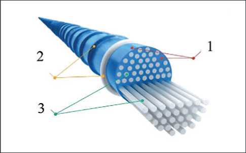
Fig.1. View of strengthened stressed composite reinforcement in section:
1 – polymer composite material;
2 – twisted thread of direct glass roving;
3 – stressed reinforcing fibers.
A method to obtain biocide suspension applied on wallpaper and wall finishings (RU 2757849 С1)
Today the task concerning disinfection of surfaces and air in public rooms, especially in medical centers, is of great importance. One of the ways to resolve this problem is the application of lacquer coatings on the basis of water-dispersed paints with nanosize particles of silver, copper or gold with increased biocide activity which protect painted surfaces from formation of bacteria and fungi as well as eliminate pathogenic microorganisms and inhibit the process of bacterial growth [2].
The aim of the invention is to create a method to obtain biocide suspension on the basis of silver nanoparticles on carbon matrix and lacquer paints, possessing
REVIEW OF NANOTECHNOLOGICAL INVENTIONS high bactericidal activity in respect to strains of different classes of microorganisms which are pathogenic for humans and mammals. The biocide suspension is to be applicable as a coating with bactericidal and fungicidal properties on the paper walls used in production and personal service rooms, in childcare centers, as well as in crowded halls, etc.
Imposed task is solved by developing method to obtain biocide suspension. These are the stages of the method:
-
1. Addition of powder of silver nanoparticles on carbon matrix with nanoparticle sizes 1–500 nm in basic liquid in such a way to provide ratio between weight percentage of silver nanoparticles on carbon matrix and basic liquid to be equal 0–5%;
-
2. Ultrasound dispersion;
-
3. Preparation of biocide suspension by retention and draining of obtained dispersion.
The invention can be used in construction and chemical industry. The invention provides high bactericidal activity respect to strains of various classes of microorganisms.
A method to obtain nanolithographic pictures with ordered structure with hyperbranched surface (RU 2757323 С1)
The invention refers to nanotechnologies, in particularly, to the methods used to form nanomaterials as nanolithographic pictures with ordered structure with hyperbranched surface and can be used to obtain new generation of nano- and microelectronic devices [3].
At present, to form lithographic pictures, including those with nanoresolution, two basic technological approaches are applied. The first one is a logical development of classical microelectronic technology concept and it is based on the usage of optical, X-ray or electron-beam lithography. Shortened length of radiation wave mode when exposing a photoresist makes it possible to create pictures in which size of certain elements is less 100 nm. The second technological approach, in its essence, is a purely nanotechnological one and is based on a probe that moves on the substrate surface and contacts with it in local areas. That results in formation of a specified spatial profile in the form of nano- or microrelief.
One of the important nanotechnological tasks is to develop new methods aimed at obtaining nanomaterials with hyperbranched surface. Such materials possess unique photocatalytic and adsorption properties, as well as high specific surface of interaction with environment, that determines their application in designing devices for nano- and microelectronics, including highly efficient gas and vacuum sensors. To obtain them, various physical and chemical methods are applied, in particularly, solgel technology. Combination of this technology with the latest methods of forming nanolithographic pictures will make it possible to produce nanomaterials with ordered structure with hyperbranched surface.
The technical result of the invention is that due to combination of probe lithography and sol-gel method nanolithographic pictures with ordered structure with hyperbranched surface are formed. That is achieved due to the following: the known method used to form nanolithographic pictures employs method of probe lithography in which mechanical impact of the probe on the substrate leads to formation of spatial profile in the form of areas of specified geometry. Additionally, sol-gel synthesis method implies that substrate surface is covered with film-forming sol on the basis of 2-aminoethanol, 2-metoxyethanol, zink acetate and sodium acetate. After that, low-temperature annealing under 80°С and photoannealing by means of ultraviolet wave radiation are performed. The result is that nanolithographic picture with ordered structure with hyperbranched surface emerges in the area of spatial profile in the form of specified shapes that act as growth points.
A method of aerosol spraying of nanoparticles in constant electric field (RU 2756323 С2)
The invention refers to creation of nanostructured coatings that consist of nanoparticles of different materials and can be used to obtain coatings with controlled anisotropic properties. The invention can be also used to design new components of photonics and optoelectronics [4]. The method of aerosol spraying of nanoparticles in constant electric field includes precipitation of colloid nanoparticles on hard substrates in constant electric field which strength is 105-108 V/m and which is created between focusing grid-cathode and heated metal anode plate-base. Spraing on the substrate is performed under the pressure 1–10 atm and coordinatewise scanning with specified rate and distance of spraying nozzle – a substrate with controlled surface area and possibility to form a thin film or layered structure due to multiple precipitation. The technical result is the improved method of aerosol spraying of nanoparticles in constant electric field which is different in the following way: when spraying colloid solutions, it allows focusing drop flow by negatively charged grid on the surface of heated substrate which efficiently evaporates liquid and provides even precipitation of nanoparticles without their further movement in a small evaporating liquid drop.
Description of the method (Fig. 2): from the metal spraying nozzle, fixed to L-shaped crossbar by means of rectangular clamp (1), under pressure supplied by compressor (1–10 atm), colloid solution with metal nanoparticles is sprayed through focusing metal grid, to which negative contact is attached to control course of projection of particles (2). The metal grid is placed under the injector nozzle at the adjustable distance to the substrate
REVIEW OF NANOTECHNOLOGICAL INVENTIONS
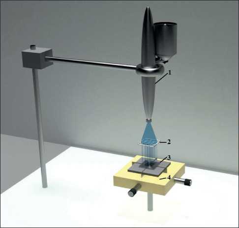
Fig. 2. A method of aerosol spraying of nanoparticles in constant electric field through which sprayed colloid solution is precipitated on the substrate, to which a positive charge is supplied, with temperature set in the range 20–100oС due to thermal element (3) located on positioning stage (4). This scheme allows changing angles of projection of particles and drops in precipitation process, as colloid particles possess negative charge. In this case, under electric field with strength 105–108 V/m, passing through the grid, all particles get acceleration towards positive contact – anode – and get focused in each cell owing to Coulomb repulsion from negatively charged grid surface. In precipitation process the particles, due to difference between their charges, are fixed on the surface (Fig. 3).
Control of spraying is conducted by means of servomotor, programmed with microcontroller, that allows
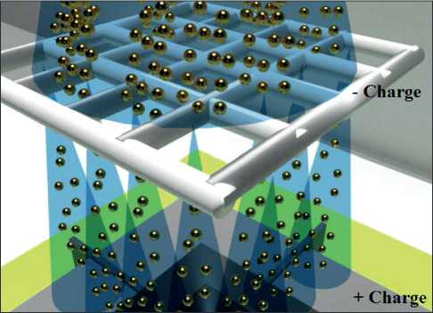
Fig. 3. In precipitation process the particles, due to difference between their charges, are fixed on the surface manipulating consumption of sprayed colloid solution. Selection of the pressure supplied by compressor is due to the fact that efficient spraying without destroying nanoparticles and their agglomerates occurs in the range 1–10 atmospheres. Rate of substrate displacement by means of positioning table varies, in dependence on the distance between spraying nozzle and the surface of precipitated layer.
A method to obtain amorphous nanostructures diamond-like coating (RU 2757303 С1)
The invention refers to technology of applying hard durable nanostructured coatings of amorphous diamondlike carbon and can be used in metal forming, mechanical engineering, medicine, solar power engineering, optoelectronics, photonics, production of liquid crystal display devices, shields with high hardness to increase performance characteristics of surface of the products used in various areas. A method to obtain amorphous nanostructures diamond-like coating consists of applying at least one layer of carbon diamond-like film by means of cathode spraying of graphite, at this, adhesive layer preliminary is formed out of the vacuum chamber. The adhesive layer is formed by applying powder of graphite, titanium, chrome, aluminum or mixture of them on detail surface and by exposing to ultrasound indentor [5].
Under the impact of ultrasound indentor the adhesive material, preliminary applied on the detail surface, diffuses through this surface, that provides high adhesive durability of the coating.
Since the adhesive layer is applied on the surface of detail out of the vacuum chamber, that reduces total time of application of dimond-like coating in vacuum chamber, rises its performance and pass-through capacity. When a large amount of articles is produced, ultrasound process of application of adhesive layer can be combined by time with application of diamond-like coating in vacuum chamber, that additionally increases pass-through capacity of the whole technological system.
A polymer composite heat-conducting pastewith nanofiber modifier (RU 2757253 С2)
The preregistered technical solution refers to the field concerning heat-conducting materials and can be used to joint heat-stressed surfaces of different details and items. The efficiency of thermal transfer depends on thermal conduction coefficient as well as square of contacting area in materials. Therefore, to provide maximum possible thermal conductivity one needs to provide dense contact between surfaces. Since surfaces of any materials are not absolutely flat, there are air gaps which dramatically decrease thermal transfer in the system. Application of heat-conducting pastes (thermal paste) is the optimal
REVIEW OF NANOTECHNOLOGICAL INVENTIONS and widely used approach to solve this problem. In concrete terms, this application for an invention is related to the method aimed at using certain composition of nanostructured mixture which is compound of binder, as a rule, organosilicic and filler (heat-conducting material). At this, the mixture possesses a wide temperature range of performance, it is incombustible, non-toxic, is not electrically conductive, it does not decay after long usage and it is cheap [6].
A modifier is preferably made of carbon nanotubes (CNT) or fibrous silica, that possess high thermal conductivity 150–3500 Watt/ (m•К), clearly defined anisotropic structure which provides formation of “heat-conducting bridges” between spherical particles and high affinity to organic binder.
The polymer composite heat-conducting paste contains heat-conducting non-organic filler in the form, for example, of aluminum nitride particles and/or graphite, and a filler in the form of organic polysiloxane. At this, polydimethylsiloxane and nanofiber modifier, taken in amount from 0.1 to 15% of mass of non-organic filler powder, are used as organic polysiloxane. Increase of content of fiber and nanofiber modifiers by more than 15% leads to the loss of mechanical characteristics and impossibility to apply heat-stressed surfaces for jointing.
A plant to provide electroimpulse controlled obtaining of nanoparticles of current conducting materials (RU 2756189 С1)
An invention refers to powder metallurgy and production of nanostructures which can be used to produce equipment for quantum informatics, radiophotonics and nanoelectronics, as well as to obtain coatings and can be implemented in additive technologies [7]. A plant to provide electroimpulse controlled obtaining of nanoparticles of current conducting materials (Fig. 4) contains a charging 3 and a discharging 8 circuit. The charging 3 circuit consists of laboratory auto-transformer (LATR) 5, input pins 1 and 2 of which are connected to electric network of varying voltage power and output – to the primary winding of high-voltage step-up transformer (HVST) 5, the secondary winding of which is connected to high-voltage electric condenser 7 via protective current-limiting resistors 6. To control performance mode, there are volt meters 14 and 15 on outputs of LATR 4 and HVST 5. Discharging circuit 8, parallel-connected to high-voltage electric condenser 7 by means of output pins of the latter, consists of electric-spark dispersion reactor 11, filled with dielectric liquid in which working dispersed electrodes with outputs 12 and 13 are immersed. The electrodes rotate relative to each other, there is a working inter-electrode gap 10 between them. The discharging circuit 8 also comprises a variable air spark discharger 9 which breakdown voltage is more than that of working
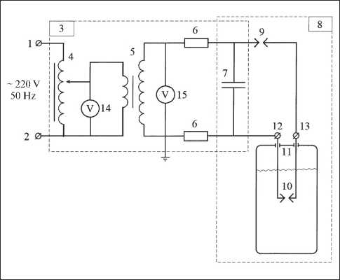
Fig. 4. A functional configuration of the plant for electroimpulse controlled obtaining of nanoparticles and nanopowders of metal and semi-conducting materials and alloys inter-electrode gap 10. The technical result provides stable generation of electric-spark discharge under small power of discharge impulses less than 100 mJ and inter-electrode gap more than 50 µm in order to obtain nanoparticles of current conducting materials, close to nanodispersed.
The technical result is achieved due to the following: the plant for electroimpulse controlled obtaining of nanoparticles and nanopowders of metal and semiconducting materials and alloys consists of rotating relative each other working dispersible electrodes, immersed in electro-spark dispergating reactor filled with dielectric liquid, charging and discharging circuits parallel-connected to each other and high-voltage electric condenser, input pins to connect charging circuit to varying voltage electric network, output pins of discharging circuit to connect to working disperse electrodes. At this, charging circuit consists of laboratory autotransformer which output is connected to the primary winding of high-voltage step-up transformer, the secondary winding of which is connected to high-voltage electric condenser via protective current-limiting resistors. The discharging circuit that consists of high-voltage electric condenser and working inter-electrode gap between working disperse electrodes also comprises a variable air spark discharger which breakdown voltage is more than that of working inter-electrode gap.
Photoelectric converter (RU 2756171 С1)
The invention refers to solar energy, in particularly, to photoelectric converters and can be used in electronic industry to convert photo energy into electrical energy. One of the main stages in production of photoelectric
REVIEW OF NANOTECHNOLOGICAL INVENTIONS converter is a formation of ohmic contacts. Decrease of transition contact resistance and increase of conductivity in contact bars of front ohmic contact makes it possible to significantly reduce ohmic losses and to rise efficiency of emission conversion into electrical energy [8].
The task of the invention is to increase electrical conductivity of contact bars of front ohmic contact due to increase of adhesion of contact layers and reduction of ohmic losses by decreasing transition contact resistance. The imposed task is achieved due to the following: photoelectric converter consists of a substrate of n-type conductivity, photosensitive А3В5 heterostructure with wide area window and a contact layer GaAs of p-type conductivity, anti-reflecting coating on the surface of wide area window in the areas free from front ohmic contact, back ohmic contact and front ohmic contact on the surface of contact layer GaAs, containing layers Ag and Au. A novelty in the photoelectric converter is that fron ohmic contact comprises successive located the first layer of nickel and chrome alloy (NiCr) with content of chrome (15–50) mass.% with thickness (5–25) nm, a layer of Ag with thickness (500–5000) nm, the second layer of NiCr alloy with content of chrome (15–50) mass. % with thickness (50–100) nm and a layer of Au with thickness (30–100) nm.
After the layers of front and back contacts have been applied, photoelectric converter is exposed to thermal treatment under the temperature (390–410)oС for (50– 70) seconds. The mode of thermal treatment for contact is determined by the condition to minimize specific transition resistance as well as to provide not deep position of metal-semiconductor interface.
A device to obtain nanoparticles from gases and liquid vapors under ultra-low temperatures (RU 2756051 С1)
The invention refers to nanotechnologies, in particularly, this device allows obtaining particles of small sizes (nanoparticles) from materials, existing under room temperature in the form of gases or vapors, condensation of which takes place on the surface of superfluid liquid [9].
The invention contains cryostat with superfluid helium as a low-temperature substrate for condensation of nanoparticles, a pipe to supply mixture of helium and required admixture, an ampoule to collect nanoparticles, a device to maintain the level of superfluid helium higher than pipe end to create low-temperature substrate for condensation of nanoparticles on the surface of superfluid helium and to prevent mixture losses in the process of formation of nanoparticles.
When the device works (Fig. 5), a flow of admixture-helium mixture (8) is supplied in condensation pipe (3) to the surface of superfluid helium in ampoule (4). The level of admixture-helium mixture in the ampoule is maintained to be constantly (10) higher than condensation
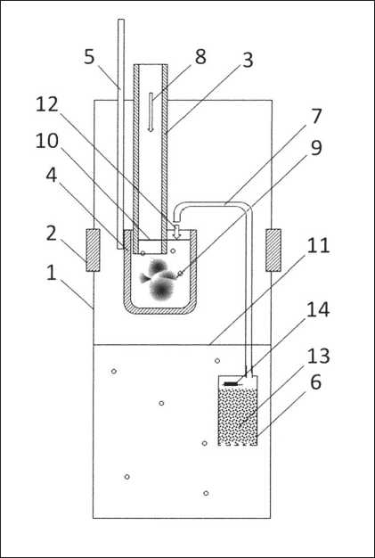
Fig. 5. A device to obtain nanoparticles from gases and liquid vapors under ultra-low temperatures: 1 – helium cryostat with vacuum isolation, 2 – windows, 3 – condensation tube, 4 – ampoule for collecting nanoparticles, 5 – stick, 6 – cryopump, 7 – pouring tube, 8 – flow of admixture-helium mixture, 9 – condensed nanoparticles, 10 – level of helium in ampoule, 11 – level of helium in cryostat, 12 – flow of pouring superfluid helium, 13 – fine powder, 14 – heater pipe end in order to prevent losses of condensed mixture. A mixture of small amount (order of several percents) of admixture (for example, gases: deuterium, methane, nitrogen or vapors of water, heavy water, spirit, etc.) and gaseous helium while travelling in condensation pipe is cooled from room temperature to helium one for several tens of seconds and nanoparticles are formed (9). At this, helium atoms prevent from forming big particles. In the mixture cooling process an intensive evaporation of superfluid helium takes place, that decreases helium level in the ampoule. If helium level is lower that bottom end of condensation pipe, condensation process stops. To maintain the constant level of superfluid helium in ampoule higher than the end of condensation pipe, a cryopump (6) was used. The principle of cryopump is based on the ability of superfluid component to flow through small gaps between particles of fine powder (13), while normal component of helium (after having been heated by heater (14) in upper
REVIEW OF NANOTECHNOLOGICAL INVENTIONS part of cryopump and transition of superfluid component into normal one) possesses big hydraulic resistance when passing through the powder. Due to increased pressure in cryopump superfluid helium raise up in pouring pipe (8), that supplies helium in ampoule (4) despite of the fact that helium level in cryostat (11) can be significantly lower than in the ampoule (10). The application of such tool as cryopump prolong time needed to accumulate nanoparticles and increases the outcome of the final product.
An accumulative device and production system(RU 2755803 С1)
A series of inventions refers to an accumulative device and production system to obtain material of carbon nanotubes. The accumulative device to collect films of carbon nanotubes or fibers of carbon nanotubes contains preliminary adjusting mechanism to control orientation of at least one beam of carbon nanotubes aggregates, a winding mechanism to wind and collect aggregates of carbon nanotubes extracted from preliminary adjusting mechanism [10].
At this, the preliminary adjusting mechanism consists of the first preliminary adjusting submechanism and the second preliminary adjusting mechanism containing at least the third wheel element to extract aggregates of carbon nanotubes. The third wheel element is made in such a way to rotate and is circled by numerous first collar steps which are present on it to adjust orientation of carbon nanotubes. The width of the first collar step is not more than 10 µm, at this, neighboring first collar steps are separated from each other with gaps which are not more than 100 µm.
Production system to obtain material of carbon nanotubes fibers of carbon nanotubes contains synthesizing device for flotation catalytic synthesis of carbon nanotube aggregates, which contains a reactor possessing at least one growing tube and the accumulative device, located on the side of delivery end of synthesizing device to collect aggregates of carbon nanotubes produced by synthesizing device. A series of inventions makes it possible to adjust mechanical, electrical and thermal properties of collected materials of carbon nanotubes.
The specialists can also be interested in the following inventions related to nanotechnologies:
-
• A method for producing a composite material with oriented carbon nanotubes [11];
-
• A method to produce polarization-sensitive nanocomposite film on the basis of cupric selenide [12];
-
• A method to produce indicator microcapsules with the use of magnetic and plasmon nanoparticles [13];
-
• Chemical compounds for coatings of nanostructures [14];
-
• Phase change materials for building construction: An overview of nano-microencapsulation [15];
-
• A method to obtain antifriction polymer composite [16];
-
• Electrochemical method to obtain nanofibers of metal copper [17];
-
• A method to obtain thermoplastic non-woven material on the basis of micro- and nanofibers from aroma polyetherimide [18];
-
• A method to determine location of polyethylene gas pipeline and places of possible illegal tapping of those pipeline [19];
-
• A composition for coating of metal products [20];
-
• A method to transfer graphene on polymer substrate [21];
-
• A method to obtain pyrocarbon coating from guanidin derivative [22];
-
• A sensitive element of luminous sensor and a method to obtain it [23];
-
• Experimental assessment of cement mortar using nano oxide compounds [24];
-
• A method to determine burning temperature of reaction multi-layered nanofilms with the effect selfpropagating high-temperature synthesis [25];
-
• A method of synthesis of antipathogenic carbon-silver nanostructured powder [26];
-
• A method to create suspension on the basis of detonation nanodiamond [27];
-
• A method to obtain modified lignosulphate agent to treat boracic solution [28];
-
• Evolution of PV technology from conventional to nanomaterials [29];
-
• A method to obtain nanopowder of iron carbide [30];
-
• A method to obtain optical semi-conducting material on the basis of nanodispersed cadmium oxide, doped with lithium [31].
CONCLUSION
One of the most challenging tasks the economy of every country face is to increase industrial competitiveness through technological upgrade. From the side of the state and companies the principal object to control in this process are the people and enterprises dealing with introduction of inventions and new technologies. Therefore, we hope that the information published in this section will be in demand and useful for specialists.
REVIEW OF NANOTECHNOLOGICAL INVENTIONS
References Inventions of scientists, engineers and specialists from different countries in the area of nanotechnologies. Part VI
- Belkin S.V., Chalenko K.А A method to obtain polymer-composite material and a composite reinforcement. RF Patent 2755343-09-15. 2021.
- Maltsev V.А., Novopashin S.А., Moiseenko V.V. A method to obtain biocide suspension applied on wallpaper and wall finishings. RF Patent 2757849-10-21. 2021.
- Averin I.А., Pronin I.А., Karmanov А.А. et al. A method to obtain nanolithographic pictures with ordered structure with hyperbranched surface. RF Patent 2757323. 2021-10-13.
- Kutrovskaya S.V., Kucherik А.О., Osipov А.V., Samyshkin V.D. A method of aerosol spraying of nanoparticles in constant electric field. RF Patent 2756323. 2021-09-29.
- Okhlupin D.N., Korolev А.V., Sinev I.V. et al. A method to obtain amorphous nanostructures diamond-like coating. RF Patent 2757303. 2021-10-13.
- Shishkin R.А., Kiseev V.M., Sazhin О.V. A polymer composite heat-conducting paste with nanofiber modifier. RF Patent 2757253. 2021-10-12.
- Diteleva А.О., Kukushkin D.Yu., Savkin А.V., Sleptsov V.V. A plant to provide electroimpulse controlled obtaining of current conducting nanoparticles. RF Patent 2756189. 2021-09-28.
- Soldatenkov F.Yu., Malevskaya А.V. Photoelectric converter. RF Patent 2756171. 2021-09-28.
- Efimov V.B., Mezhov-Deglin L.P., Lokhov A.V. A device to obtain nanoparticles from gases and liquid vapors under ultra-low temperatures. RF Patent 2756051. 2021-09-24.
- Li Da, Jin Hehua, Li Jinwan et al. An accumulative device and production system. RF Patent 2755803. 2021-09-21.
- Ivanov L.A., Xu L.D., Razumeev K.E., Feoktistova V.M., Prokopiev P.S. Inventions of scientists, engineers and specialists from different countries in the area of nanotechnologies. Part V. Nanotechnologies in Construction. 2021; 13(5): 311–318. https://doi.org/10.15828/2075-8545-2021-13-5-311-318.
- Miheev G.M., Kogai V.Ya.-S., Styapshin V.M., Mogileva T.N. A method to produce polarization-sensitive nanocomposite film on the basis of cupric selenide. RF Patent 2758150. 2021-10-26.
- Dubovik А.Yu., Kurshanov D.А., Rogach A., Arefina I.А. A method to produce indicator microcapsules with the use of magnetic and plasmon nanoparticles. RF Patent 2758098. 2021-10-26.
- Akselsson О., Sansone А. Chemical compounds for coatings of nanostructures. RF Patent 2757904. 2021-10-22.
- Ivanov L.A., Xu L.D., Pisarenko Zh.V., Nguyen C.T., Muminova S.R. Inventions of scientists, engineers and specialists from different countries in the area of nanotechnologies. Part IV. Nanotechnologies in Construction. 2021; 13(4): 242–251. Available from: doi: 10.15828/2075-8545-2021-13-4-242-251.
- Goryainov G.I., Goryainov А.G., Sarakuz О.N. A method to obtain antifriction polymer composite. RF Patent 2757862. 2021-10-21.
- Karfidov E.А., Nikitina E.V., Kazakovtseva N.А. et al. Electrochemical method to obtain nanofibers of metal copper. RF Patent 2757750. 2021-10-21.
- Svetlichny V.M., Vaganov G.V., Myagkova L.А. et al. A method to obtain thermoplastic non-woven material on the basis of micro- and nanofibers from aroma polyetherimide. RF Patent 2757442. 2021-10-15.
- Ivanov L.A., Xu L.D., Bokova E.S., Demenev A.V., Ivanov V.A. Inventions of scientists, engineers and specialists from different countries in the area of nanotechnologies. Part III. Nanotechnologies in Construction. 2021; 13(3): 158–165. Available from: doi: 10.15828/2075-8545-2021-13-3-158-165.
- Li R.I., Psarev D.N., Kiba M.R. et al. A composition for coating of metal products. RF Patent 2757271. 2021-10-12.
- Grebenko А.K., Aitkulova А.D., Krasnikov D.V., Nasibulin А.G. A method to transfer graphene on polymer substrate. RF Patent 2757239. 2021-10-12.
- Antishin D.V., Shalygina Т.А., Pehotin K.V. A method to obtain pyrocarbon coating from guanidin derivative. RF Patent 2756308. 2021-09-29.
- Pavlov S.А., Pavlov А.S., Maksimova Е.Yu. et al. A sensitive element of luminous sensor and a method to obtain it. RF Patent 2757012. 2021-10-08.
- Ivanov L.A., Xu L.D., Bokova E.S., Ishkov A.D., Muminova S.R. Nanotechnologies: are view of inventions and utility models. Part V. Nanotechnologies in Construction. 2020; 12(6): 331–338. Available from: doi: 10.15828/2075-8545-2020-12-6-331-338.
- Korzh I.А. A method to determine burning temperature of reaction multi-layered nanofilms with the effect self-propagating high-temperature synthesis. RF Patent 2757067. 2021-10-11.
- Novopashin S.А., Maltsev V.А. A method of synthesis of antipathogenic carbon-silver nanostructured powder. RF Patent 2755619. 2021-09-17.
- Plotnikov V.А., Makarov S.V., Bogdanov D.G., Shutkin А.А. A method to create suspension on the basis of detonation nanodiamond. RF Patent 2757049. 2021-10-11.
- Kulyashova I.N., Badikova А.D., Fedina R.А., Begalieva R.S. A method to obtain modified lignosulphate agent to treat boracic solution. RF Patent 2756820. 2021-10-06.
- Ivanov L.A., Xu L.D., Bokova E.S., Ishkov A.D., Muminova S.R. Inventions of scientists, engineers and specialists from different countries in the area of nanotechnologies. Part I. Nanotechnologies in Construction. 2021; 13(1): 23–31. Available from: doi: 10.15828/2075-8545-2021-13-1-23-31.
- Zhigach А.N., Leipunsky I.О., Berezkina N.G. et al. A method to obtain nanopowder of iron carbide. RF Patent 2756555. 2021-10-01.
- Krasilnikov V.N., Baklanova I.V., Tyutyunnik A.P. A method to obtain optical semi-conducting material on the basis of nanodispersed cadmium oxide, doped with lithium. RF Patent 2754888. 2021-09-08.
