Low Noise Amplifier for 2.45 GHz Frequency Band at 0.18 μm CMOS Technology for IEEE Standard 802.11 b/g WLAN

Author: Viranjay M. Srivastava, Ravinder Kumar
Journal: International Journal of Intelligent Systems and Applications(IJISA) @ijisa
Article in issue: 9 vol.4, 2012.
Free access
This paper presents the design of low noise amplifier (LNA) at 2.45 GHz and integrated at 0.18 µm RF CMOS process technology. This type of LNA at 2.45 GHz is use in the Bluetooth receiver. The proposed method is useful to optimize noise performance and power gain while maintaining good input and output matching. The amplifier is designed to be used as first stage of a receiver for wireless communication. The main aim of designer is to achieve low noise figure with improved gain with the help of CMOS technology by using single stage n-MOS amplifier. The simulation results show a forward gain of 14.0 dB, a noise-figure of 0.5 dB and stability factor is approximate unity, in which the circuit operates at 14.2 mA drain current with supply voltage of 3.5 V and biasing voltage of 1.5 V.
Advanced design system, Low noise amplifier, Input and output matching, RFIC, VLSI
Short address: https://sciup.org/15010308
IDR: 15010308
Text of the scientific article Low Noise Amplifier for 2.45 GHz Frequency Band at 0.18 μm CMOS Technology for IEEE Standard 802.11 b/g WLAN
Published Online August 2012 in MECS
A low noise amplifier (LNA) requirement is important with regard to system performance due to growth of modern communication systems [1-4]. Low noise amplifier is use as the first block in front-end of receiver in wireless communication to amplify the desired band of signals without adding significant noise to the signal. This amplifier is a non-linear characteristic device and causes two main problems one is blocking and other is inter-modulation [5-7]. Low noise amplifier is used to reduce the external as well as internal noise [8]. The LNA can be designed and fabricated in user defined CMOS technology as topologies are the generalized schematic of circuit [9, 10]. The complete circuit can be designed using analog RF circuit designing procedure for desired frequency band and specifications. We have used an inductive source degenerated LNA topology for the application in WCDMA have minimum noise figure [11]. The design of matching network circuit is called the topology of LNA. The interference always occurs at the receiver end. Signal amplification is typically focused at the analog baseband stage.
The circuit requires current reusing and transformer feedback techniques to reduce the current consumption while optimizing the input matching and noise performance [12]. The common-gate transformer feedback transconductance boosting is used to minimize the current consumption then gain is doubled due to the sum of n-MOS and p-MOS transconductances. The main function of the LNA is mutually dependent on a set of design parameter values. LNA design with deep n-well into a fully integrated LNA with forward biasing exhibits better power gain and noise-figure performance [13]. The smallest signal that can be received at the receiver end whose defines the receiver sensitivity. The largest signal can be received by a receiver establish the upper power level limit whose can be controlled by the system while preserving voice quality.
The RF front-end circuit is shows in figure 1. The LNA follows the antenna and its output drives the mixer. It is first block after antenna in receiver frontend [14, 15]. Its main function is to amplify low signals without adding noise.
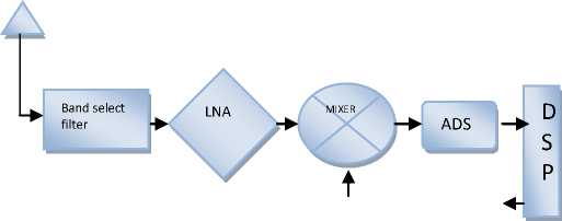
Fig.1 RF front-end circuit
In this paper, we have designed a single stage LNA circuit and input/output matching technique for IEEE 802.11 and Bluetooth standard over a frequency band of 2.45 GHz at 0.18 µm CMOS technology. Bluetooth supports a very short range approximately 10 meters. The proposed CMOS LNA is designed for IEEE standard 802.11(b) and 802.11(g). The organization of the paper is as follows: The IEEE standard WLAN are discussed in the Section II. The designs of LNA are given in the Section III and the simulated results are discussed in the Section IV. Finally, Section V concludes the work.
CMOS Technology for IEEE Standard 802.11 b/g WLAN
-
II. IEEE Standard (802.11b/g) WLAN
The Institute of Electrical and Electronics Engineers (IEEE) created the WLAN 802.11(b) standard in Sept. 1999. Standard 802.11(b) supports the bandwidth up to 11 Mbps. These have lowest cost, signal range is 35 meter indoor and 140 meter outdoor and not easily obstructed.
In June 2003, WLAN supports the standard 802.11(g). These standard attempts to combine the best of both 802.11(a) and 802.11(g). This standard 802.11(g) supports the bandwidth up to 54 Mbps [16]. These have fast maximum speed and signal range is also better. Table I summarizes the important specification of WLAN standards 802.11(b) and 802.11(g).
In the fully integrated two stages LNA, use the resistive shunt-feedback, simplified band-pass filter circuit to achieve wide input impedance matching [18, 19]. The cascoded CMOS topology is widely used in LNA designing to achieve the maximum gain. In the cascoded CMOS LNA, noise-figure (NF) and linearity of a low noise amplifier is directly affected by the gate width and gate-source voltage of common-source transistor. The circuit structure is shown in figure 2.
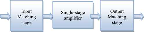
Fig.2 Low noise amplifier structure
Table I Summarized WLAN 802.11 (b/g) Standards
|
IEEE Standard 802.11(b) |
IEEE Standard 802.11(g) |
|
|
Release |
Sept. 1999 |
June 2003 |
|
Frequency |
2.4 GHz |
2.4GHz |
|
Max. data rate |
11 Mbps / 5.5 Mbps |
54 Mbps / 24 Mbps / 12 Mbps |
|
Modulation |
DSSS |
DSSS, OFDM |
|
Indoor range |
35 meter |
38 meter |
|
Output range |
140 meter |
140 meter |
This circuit structure of the proposed LNA consists of input matching stage, single stage amplifier and output matching stage. In this paper, we use the inductively degenerated common source topology as shown in figure 3.
-
III. LNA Circuit Design
The LNA have mainly three sections to be designed in complete circuit.
-
1. Input matching network
-
2. Main transistor section
-
3. Output matching network
The input matching network is used to make the input return loss (S 11 ) minimized without introducing additional noise. The input matching circuit that terminates the transistor to gamma optimum (Γ out ) which represents the input impedance of the transistor for the best noise matches. Attenuation is lowest at 77 Ω and power handling capability is highest at 30 Ω. So, the compromise between these two parameters gives the 50 Ω resistive input impedance to design a LNA [17].
Main transistor section ensures a high gain, high linearity and low noise factor at the time of input and output matching. The last step in LNA design involves output matching. The input and output impedance matching is required to maximize the power transfer and minimize the reflections. Smith chart is used for impedance matching. According to maximum power transfer theorem, maximum power delivered to the load when the impedance of load is equal to the complex conjugate of the impedance of source (Z S = Z L *).
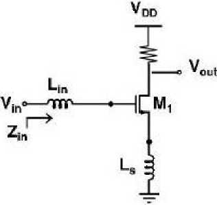
Fig.3 Single stage inductively degenerated common source configuration
This topology has been best choice for many frequency bands due to its noise and gain performance. By the use of changing the source degeneration inductor (L S ), we can be improved input matching (S 11 ). The input impedance of single-stage inductive degeneration CMOS LNA is expressed by ( L in =L g ):
Zin = MLLg + Ls ) + ■ c + gm s (1)
I to Cgs Cgs
For the input impedance matching, the gate-source capacitance (Cgs) of transistor is used. By the use of parallel LC network, it will neither increase power consumption nor degrade quality factor (Q L ) [19, 20]:
Q l =
^ o C gs z o
where ω 0 is the resonant frequency and is defined as in the following equation:
Ю
o
( Ls + Lin ) Cgs
CMOS Technology for IEEE Standard 802.11 b/g WLAN gm
® T =
Cgs
After that condition, we can be drive output impedance of inductive degeneration CMOS LNA:
Zo ® TLs
At resonance, the voltage across the capacitor and the short circuit output current is defined in equation:
C. Impedance Matching
Impedance matching at input and output port done by using smith chart technique, by properly adjusting the value of inductance and capacitance at input and output side, we have managed to match impedance with the terminating resistance of 50 Ω. Γ s and Γ L is the source and load reflection coefficient respectively. Input and output reflection coefficient is Γ in and Γ out respectively shown in following equations:
Vgs QLVs and iout gmVgs (6)
s 12 s 21Г L in s 11 + 1 -
1 — s 22Г L
where gm is the transconductance of the device.
s12s2irs_ out s 22 I -
1 — s 1i r s
-
A. Transconductance
The transconductance of the MOS transistor depends on the bias current and device geometry:
g m = 2kwirD (7)
where k = H nCox . The relationship of the input to the output of an amplifier usually expressed as a function of the input frequency is called the transfer function of the amplifier. The common-gate LNA achieves high gain and low noise-figure.
It realizes the input matching through a parallel LC network for fully integrated CMOS LNA with on-chip spiral inductors [3, 21, 22]. Inductive degeneration (L S ) also improves the linearity by use of a negative series feedback.
When we use current reuse topology in LNA then we can reduce the power consumption while preserve high-gain. But this topology requires a DC bias as well as biasing resistor then they will create extra noise and signal leakage [8]. The current reuse topology can be used with any circuit like common-source and common- gate.
-
D. Stability Factor (K)
Amplifier is not reliable when it is instable condition. The stability of a circuit is characterized by stern stability factor. The circuit is stable only when K>1 and Δ<1. When the input and output reflection coefficients are less than one then we determined the absolute stability factor:
K =
1 + A2 - 5 2 - 5 222
2 S 11 S 22
A = 5 11 5 22
S 12 S 21
When K<1, then Smith chart is stable but when the K<0, then the Smith chart is unstable [4].
-
E. Transducer Power Gain
It is the ratio of output signal to the input signal and also signals amplification capability of LNA. The CMOS LNA drives the transducer power gain whose power delivered to the load divided by power available from source:
-
B. S-parameters
It is refers to RF output voltage verses input voltage in the RFIC and describes the relationship between the two or more port network.
G T =
1 — 1Г s i2 I s P = 1 —Г L l2
1 1 - » 11 Г s 12 21 1 - s 22 Г L I2
In the term of RFIC, S11and S22 is called reflections coefficient. S21 and S12 are called transmission coefficient. S 11 and S 22 are used to calculate the input and output reflection in the circuits [23]. S 21 and S 12 are used to calculate the forward and reverse voltage gain in dB as shown in the figure 4.
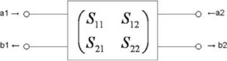
Fig.4 S-parameters of two port network
-
F. Noise-Figure
It is the ratio of output SNR to the input SNR in dB:
SNR
In the cascaded form the noise-factor (F) is given as:
F total = FLNA +
G LNA
-
G. Linearity
Linearity of LNA is most important in a wireless receiver to reduce the inter-modulation distortion. The
linearity is expressed by the 1 dB compression point and inter-modulation product (IP3). When the input signal is increased, a point is reached where the power of the signal is not amplified by the same amount as the smaller signal at the output. At this point where the input signal is amplified by an amount 1 dB less than the small signal gain, these are called 1 dB compression point. IIP 3 (input inter-modulation product) is proportional to the ratio of the first and third derivatives of the transfer characteristic. IIP 3 is expressed as:
IIP 3
4 g m 1
^ 3 g m 3
H. Spurious-free dynamic range (SFDR)
These are use as a specific measure of dynamic range between a lower bound and upper bound of the signal. The Noi as the input referred noise power in dB. The input-referred IM3 power N0. SFDR is expressed as:
SFDR = 2[ OIP - N ]
3 3 o (17) = 2 [ IIP 3 - N oi ]
SFDR is bounded on one end by IIP3 and on the other by the noise floor .
-
IV. Simulation Results
This simulation section presents the measured results of the single-stage inductive degenerated common source CMOS LNA whose operating at the 2.45 GHz frequency band. This is implemented based on 0.18 µm CMOS technology. The measured S-parameters are shown in figure 5 to figure 9.
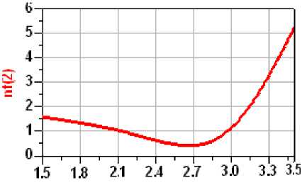
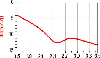
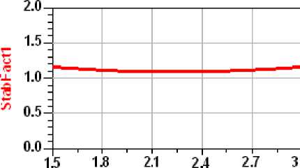
The CMOS LNA was designed at 2.45 GHz. The forward gain (S21) is 14.0 dB at 2.45 GHz frequency band shown in the figure 5. The designed LNA also shows a 0.5 dB noise-figure in figure 6. The input return loss (S 11 ) and output return loss (S 22 ) is -10 dB and -13 dB respectively shown in the figures 7 and figure 8. And the stability factor very closed to 1 dB is shown in the figure 9. The results shows that the S 11 <1 and S 22 <1 whose fulfils the stability condition. Figure the best impedance matching for high forward gain and low noise at 2.45 GHz frequency range.
The lowest F min is 0.3 dB obtained at 2.7 GHz as shown in the figure 6. But we were working at 2.45 GHz so we use the value of noise-figure at 2.45 GHz.
A forward gain simulation was performed on the LNA, and results are shown in the figure 5. When we measured result better at frequency 2.6 GHz that is forward gain of approximately 15 dB and noise-figure of 0.3 dB. But we will see all result at 2.45 GHz, because this type of frequency used in many applications.
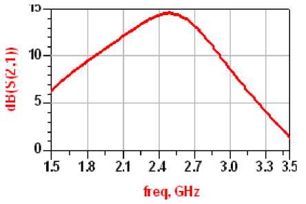
Fig.5 Power gain (S 21 ) of the LNA and achieves a forward gain (S 21 ) of 14.0 dB at 2.45 GHz.
freq, GHz
Fig.6 Noise figure of the LNA and achieves a NF of 0.5dB at 2.45 GHz.
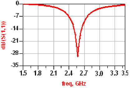
Fig.7 Input reflection coefficient (S 11 ) of the LNA. S 11 is -10 dB at
2.45 GHz.
freq, GHz
Fig.8 Output reflection coefficient (S 22 ) of the LNA. S 22 is -13 dB at 2.45 GHz.
CMOS Technology for IEEE Standard 802.11 b/g WLAN
freq, GHz
Fig.9 Stability factor (K) of an LNA at 2.45 GHz.
-
V. Conclusions
In this paper, design and implementation of a Low noise amplifier based on inductively degenerated common source topology at 2.45 GHz were presented. The LNA has been designed in a 0.18µm CMOS technology. An ADS was used for circuit design and simulation and 0.18 µm CMOS technology are used. At 3.5 V supply, LNA achieves a forward gain, noise figure and reflection coefficient operating at 14.2 mA drain current. Summary of the proposed LNA performance is shown in Table II.
A better noise and gain performance were achieved. A power gain of 14.0 dB and noise figure of 0.5 dB were obtained for the proposed LNA. Input reflection (S 11 ) and output reflection coefficients (S 22 ) of -10 dB and -13 dB respectively were achieved. Low noise amplifier is used in IEEE 802.11b/g standards for wireless local area network. They are now also used for communication like Wi-Fi and Bluetooth applications [24-26].
Table II. Summary of the proposed LNA performance
|
Parameters |
Measured Results |
|
Frequency |
2.45 GHz |
|
Power gain (S21) |
14.0 dB |
|
Noise-figure (NF) |
0.5 dB |
|
Drain current |
14.2 mA |
|
Supply voltage |
3.5 V |
Acknowledgement
The authors would like to thank Prof. G. Singh, Department of Electronics and Communication Engineering, Jaypee University of Information Technology, Solan, India, who permit to take the reference of their work related to Silicon RF CMOS Technology. The authors also thank Prof. K. S. Yadav, Sr. Scientist, CEERI, Pilani, India for many insightful discussions.
References Low Noise Amplifier for 2.45 GHz Frequency Band at 0.18 μm CMOS Technology for IEEE Standard 802.11 b/g WLAN
- Yu Lin Wei and Jun De Jin, “A low power low noise amplifier for K-band applications,” IEEE Microwave and Wireless Components Letters, vol. 19, no. 2, pp. 116-118, Feb. 2009.
- A. Meaamar, Boon Chirn Chye, Man Anh, and Yeo Kiat Seng, “A 3 to 8 GHz low noise CMOS amplifier,” IEEE Microwave and Wireless Components Letters, vol. 19, no. 4, pp. 245-247, April 2009.
- Roee Ben Yishay, Sara Stolyarova, Shye Shapira, Moshe Musiya, David Kryger, Yossi Shiloh, and Yael Nemirovsky, “A CMOS low noise amplifier with integrated front-side micro-machined inductor,” Microelectronics Journal, vol. 42, no. 5, pp. 754-757, May 2011.
- Ravinder Kumar, Munish Kumar, and Viranjay M. Srivastava, “Design and noise optimization for a RF low noise amplifier,” Int. J. of VLSI Design and Communication Systems, vol. 3, no. 2, pp. 165-173, April 2012.
- Nazif Emran Farid, Arjuna Marzuki, and Ahmad Ismat,“A variable gain 2.5 GHz CMOS low noise amplifier for mobile wireless communications,” Proc. of 9th IEEE Int. Conf. of communications, Malaysia, 15-17 Dec. 2009, pp. 885-889.
- Wei Guo and Daquan Huang, “The noise and linearity optimization for 1.9 GHz CMOS low Noise Amplifier,” Proc. of IEEE Asia Pacific Conf. on ASIC, Taiwan, 6 - 8 Aug. 2002, pp. 253-257.
- Jose Carlos Pedro and Nuno Borges Carvalho, Intermodulation distortion in microwave and wireless circuits, Artech Publication House, 1st Ed., 2003.
- Bo Huang, Chi Hsueh Wang, Chung Chun Chen, Ming Fong Lei, Pin Cheng Huang, Kun You Lin, and Huei Wang , “Design and analysis for a 60 GHz low noise amplifier with RF ESD protection,” IEEE Trans. on Microwave Theory and Techniques, vol. 57, no. 2, pp. 298-305, Feb. 2009.
- Viranjay M. Srivastava, K. S. Yadav, and G. Singh, “Analysis of drain current and switching speed for SPDT switch and DPDT switch with proposed DP4T RF CMOS switch,” J. of Circuits, Systems and Computers, vol. 21, no. 4, pp. 1-18, June 2012.
- Viranjay M. Srivastava, K. S. Yadav, and G. Singh, “Design and performance analysis of double-gate MOSFET over single-gate MOSFET for RF switch,” Microelectronics Journal, vol. 42, no. 3, pp. 527-534, March 2011.
- Norlaili, Tun Zainal and Azni Zulkifli, “A 1.4 dB noise figure CMOS LNA for WCDMA application,” Proc. of IEEE RF and Microwave Conf., Malaysia, 12-14 Sept. 2006, pp. 143-148.
- Wenjian Chen, Tino Copani, Hugh J. Barnaby, Sayfe Kiaei, “A 0.13 µm CMOS ultra-low power front-end receiver for wireless sensor networks,” Proc. of IEEE Radio Frequency Integrated Circuits Symposium, Honolulu, 3-5 June 2007, pp. 105-108.
- S. F. Wan Muhamad Hatta, N. Soin, “Performance of the forward-biased RF LNA with deep n-well n-MOS transistor,” Proc. of IEEE Int. Conf. on Semiconductor Electronics, Malaysia, 25-17 Nov. 2008, pp. 466-469.
- Viranjay M. Srivastava, K. S. Yadav, and G. Singh, “Design and performance analysis of cylindrical surrounding double-gate MOSFET for RF switch,” Microelectronics Journal, vol. 42, no. 10, pp. 1124-1135, Oct. 2011.
- Viranjay M. Srivastava, K. S. Yadav, and G. Singh, “Analysis of double gate CMOS for double-pole four-throw RF switch design at 45-nm technology,” J. of Computational Electronics, vol. 10, no. 1-2, pp. 229-240, June 2011.
- Massimo Brandolini, Paolo Rossi, Danilo Manstretta and Francesco Svelto, “Toward multi-standard mobile terminals-fully integrated receivers requirements and architectures,” IEEE Trans. on Microwave Theory and Techniques, 2005, pp. 1026-1038.
- Thomas H. Lee, The design of CMOS radio-frequency integrated circuits, Cambridge Univ. Press, 2nd Ed., 2004.
- Man Long Her, Hao Chih Hsu, Hsin Hung Lin, Tseng Hsow Yuan and Shun Ping Chan, “Design and implementation of LNA for 2 to 6 GHz WIMax system,” Proc. of 15th IEEE Asia Pacific Conf. on Communications, China, 8-10 Oct. 2009, pp. 426-429.
- Hosein Alavi Rad, Goodarz Cheraghi and Soheil Ziabakhsh, “A low power CMOS LNA for 2.45 GHz band IEEE 802.15.4 standard in 0.18µm technology,” Proc. of 5th IEEE European Conf. on Circuits and Systems for Communications, Serbia, 23-25 Nov. 2010, pp. 78-81.
- Hsieh Hung Hsieh, “A 40 GHz low noise amplifier with a positive-feedback network in 0.18 μm CMOS,” IEEE Trans. on Microwave Theory and Techniques, vol. 57, no. 8, pp. 1895-1902, Aug. 2009.
- Kiat Seng Yeo, Manh Anh Do, and Chirn Chye Boon, Design of CMOS RF integrated circuits and systems, World Scientific Publications, 1st Ed., 2010.
- Y. S. Wang and L. H. Lu, “5.7 GHz low power variable gain LNA in 0.18 µm CMOS,” Electronics Letters, vol. 41, no. 2, pp. 66-68, Jan. 2005.
- Viranjay M. Srivastava, K. S. Yadav, and G. Singh, “Capacitive model and S-parameters of double-pole four-throw double-gate RF CMOS switch,” Int. J. of Wireless Engineering and Technology, vol. 2, no. 1, pp. 15-22, Jan. 2011.
- Mu Chun Wang, Hsin Chia Yang, and Yi Jhen Li, “Minimization of cascade low noise amplifier with 0.18 μm CMOS process for 2.4 GHz RFID applications,” Electronics and Signal Processing, Lecture Notes in Electrical Engineering, vol. 97, pp. 571-578, 2011.
- Lawrence Harte, Introduction to bluetooth, Althos Publications, 2nd Ed., 2009.
- Chang Hsi Wu and Yu Po Lin, “A low power CMOS low noise amplifier for UWB applications,” Proc. of IEEE Int. Conf. on Ultra Wideband, China, 20-23 Sept. 2010, pp. 1328-1331.
